CN100571489C - Method of forming a printed circuit board - Google Patents
Method of forming a printed circuit board Download PDFInfo
- Publication number
- CN100571489C CN100571489C CNB2005100927278A CN200510092727A CN100571489C CN 100571489 C CN100571489 C CN 100571489C CN B2005100927278 A CNB2005100927278 A CN B2005100927278A CN 200510092727 A CN200510092727 A CN 200510092727A CN 100571489 C CN100571489 C CN 100571489C
- Authority
- CN
- China
- Prior art keywords
- substrate
- circuit board
- forming
- printed circuit
- layer
- Prior art date
- Legal status (The legal status is an assumption and is not a legal conclusion. Google has not performed a legal analysis and makes no representation as to the accuracy of the status listed.)
- Expired - Lifetime
Links
Images


Classifications
-
- H—ELECTRICITY
- H05—ELECTRIC TECHNIQUES NOT OTHERWISE PROVIDED FOR
- H05K—PRINTED CIRCUITS; CASINGS OR CONSTRUCTIONAL DETAILS OF ELECTRIC APPARATUS; MANUFACTURE OF ASSEMBLAGES OF ELECTRICAL COMPONENTS
- H05K3/00—Apparatus or processes for manufacturing printed circuits
-
- G—PHYSICS
- G02—OPTICS
- G02B—OPTICAL ELEMENTS, SYSTEMS OR APPARATUS
- G02B6/00—Light guides; Structural details of arrangements comprising light guides and other optical elements, e.g. couplings
- G02B6/24—Coupling light guides
- G02B6/42—Coupling light guides with opto-electronic elements
- G02B6/43—Arrangements comprising a plurality of opto-electronic elements and associated optical interconnections
-
- G—PHYSICS
- G02—OPTICS
- G02B—OPTICAL ELEMENTS, SYSTEMS OR APPARATUS
- G02B6/00—Light guides; Structural details of arrangements comprising light guides and other optical elements, e.g. couplings
- G02B6/02—Optical fibres with cladding with or without a coating
-
- G—PHYSICS
- G02—OPTICS
- G02B—OPTICAL ELEMENTS, SYSTEMS OR APPARATUS
- G02B6/00—Light guides; Structural details of arrangements comprising light guides and other optical elements, e.g. couplings
- G02B6/10—Light guides; Structural details of arrangements comprising light guides and other optical elements, e.g. couplings of the optical waveguide type
- G02B6/12—Light guides; Structural details of arrangements comprising light guides and other optical elements, e.g. couplings of the optical waveguide type of the integrated circuit kind
- G02B6/13—Integrated optical circuits characterised by the manufacturing method
- G02B6/138—Integrated optical circuits characterised by the manufacturing method by using polymerisation
-
- G—PHYSICS
- G02—OPTICS
- G02B—OPTICAL ELEMENTS, SYSTEMS OR APPARATUS
- G02B6/00—Light guides; Structural details of arrangements comprising light guides and other optical elements, e.g. couplings
- G02B6/24—Coupling light guides
- G02B6/26—Optical coupling means
- G02B6/264—Optical coupling means with optical elements between opposed fibre ends which perform a function other than beam splitting
- G02B6/266—Optical coupling means with optical elements between opposed fibre ends which perform a function other than beam splitting the optical element being an attenuator
-
- H—ELECTRICITY
- H05—ELECTRIC TECHNIQUES NOT OTHERWISE PROVIDED FOR
- H05K—PRINTED CIRCUITS; CASINGS OR CONSTRUCTIONAL DETAILS OF ELECTRIC APPARATUS; MANUFACTURE OF ASSEMBLAGES OF ELECTRICAL COMPONENTS
- H05K1/00—Printed circuits
- H05K1/02—Details
- H05K1/0274—Optical details, e.g. printed circuits comprising integral optical means
-
- G—PHYSICS
- G02—OPTICS
- G02B—OPTICAL ELEMENTS, SYSTEMS OR APPARATUS
- G02B6/00—Light guides; Structural details of arrangements comprising light guides and other optical elements, e.g. couplings
- G02B6/10—Light guides; Structural details of arrangements comprising light guides and other optical elements, e.g. couplings of the optical waveguide type
- G02B6/12—Light guides; Structural details of arrangements comprising light guides and other optical elements, e.g. couplings of the optical waveguide type of the integrated circuit kind
- G02B2006/12166—Manufacturing methods
- G02B2006/12173—Masking
-
- G—PHYSICS
- G02—OPTICS
- G02B—OPTICAL ELEMENTS, SYSTEMS OR APPARATUS
- G02B6/00—Light guides; Structural details of arrangements comprising light guides and other optical elements, e.g. couplings
- G02B6/10—Light guides; Structural details of arrangements comprising light guides and other optical elements, e.g. couplings of the optical waveguide type
- G02B6/12—Light guides; Structural details of arrangements comprising light guides and other optical elements, e.g. couplings of the optical waveguide type of the integrated circuit kind
- G02B2006/12166—Manufacturing methods
- G02B2006/12176—Etching
-
- H—ELECTRICITY
- H05—ELECTRIC TECHNIQUES NOT OTHERWISE PROVIDED FOR
- H05K—PRINTED CIRCUITS; CASINGS OR CONSTRUCTIONAL DETAILS OF ELECTRIC APPARATUS; MANUFACTURE OF ASSEMBLAGES OF ELECTRICAL COMPONENTS
- H05K2203/00—Indexing scheme relating to apparatus or processes for manufacturing printed circuits covered by H05K3/00
- H05K2203/01—Tools for processing; Objects used during processing
- H05K2203/0147—Carriers and holders
- H05K2203/016—Temporary inorganic, non-metallic carrier, e.g. for processing or transferring
Landscapes
- Physics & Mathematics (AREA)
- General Physics & Mathematics (AREA)
- Optics & Photonics (AREA)
- Engineering & Computer Science (AREA)
- Microelectronics & Electronic Packaging (AREA)
- Manufacturing & Machinery (AREA)
- Optical Integrated Circuits (AREA)
- Structure Of Printed Boards (AREA)
Abstract
提供了形成具有光学功能的印刷电路板的方法。该方法包括:(a)提供第一印刷电路板基底;(b)在与所述印刷电路板基底分开的第二基底上形成包含覆层和核的光波导结构,其中,所述光波导结构包含含硅材料;(c)使所述光波导结构与第二基底分离;(d)将所述光波导结构粘附到所述印刷电路板基底上。本发明特别适用于电子工业和光电子工业,用以形成混合印刷电路板。
A method of forming an optically functional printed circuit board is provided. The method comprises: (a) providing a first printed circuit board substrate; (b) forming an optical waveguide structure comprising a cladding and a core on a second substrate separate from the printed circuit board substrate, wherein the optical waveguide structure comprising a silicon-containing material; (c) separating the optical waveguide structure from a second substrate; (d) adhering the optical waveguide structure to the printed circuit board substrate. The invention is particularly suitable for use in the electronics and optoelectronics industries for forming hybrid printed circuit boards.
Description
技术领域 technical field
本发明一般涉及印刷电路板(PCB)。具体地说,本发明涉及形成具有光学功能的印刷电路板的方法,该方法将形成在与所述印刷电路板分开的基底上的光波导结合到所述印刷电路板中。The present invention generally relates to printed circuit boards (PCBs). In particular, the present invention relates to a method of forming an optically functional printed circuit board incorporating into the printed circuit board an optical waveguide formed on a substrate separate from the printed circuit board.
背景技术 Background technique
光波导包括核和包围核的覆层,由于与覆层相比具有更高的折射率,在核中进行光辐射传播。嵌入的光波导可通过以下方法形成在印刷电路板基底上:在基底上涂覆第一覆层,在第一覆层上涂覆核层,使核层图案化以形成一个或多个核结构,以及在第一核层和核结构上形成第二覆层。通常,使用光致抗蚀剂通过标准光刻法和蚀刻工艺,或者通过曝光并显影可光学成像的核层来使波导核层图案化。例如,Shelnut等的美国专利6,731,857和美国公开申请US20040105652公开了用倍半硅氧烷化学方法在印刷电路板上形成嵌入的光波导。The optical waveguide comprises a core and a cladding surrounding the core, in which the optical radiation propagates due to the higher refractive index compared to the cladding. Embedded optical waveguides can be formed on a printed circuit board substrate by coating the substrate with a first cladding layer, coating the first cladding layer with a core layer, and patterning the core layer to form one or more core structures , and forming a second cladding layer on the first core layer and the core structure. Typically, the waveguide core layer is patterned by standard photolithography and etching processes using photoresist, or by exposing and developing an optically imageable core layer. For example, US Patent 6,731,857 to Shelnut et al. and US Published Application US20040105652 disclose the formation of embedded optical waveguides on printed circuit boards using silsesquioxane chemistry.
在与其它电路板工艺相同的位置上形成光学层会对所得的光学结构产生有害的影响。例如,许多标准电路板制作工艺,如电镀和钻孔工艺,会产生颗粒和其它形式的污染物。这种污染物会在波导结构的形成过程中掺入到波导层中,从而例如通过由光散射和/或吸收增加光损失而对波导的透光性能产生不利的影响。这对于波导核层尤其成问题。所述污染物还会在核的图案化过程中造成缺陷,因为与标准PCB制作所用的一般图案化工艺相比,波导结构通常需要更高分辨率的图案化工艺。因此,就需要能在没有其它电路板制造工艺所产生的污染物的环境中制造波导的方法。Forming the optical layer in the same location as other circuit board processes can have detrimental effects on the resulting optical structure. For example, many standard circuit board fabrication processes, such as plating and drilling processes, generate particles and other forms of contamination. Such contaminants can be incorporated into the waveguide layer during formation of the waveguide structure, thereby adversely affecting the light transmission properties of the waveguide, for example by increasing light loss through light scattering and/or absorption. This is especially problematic for waveguide cores. Said contaminants can also cause defects during the patterning of the core, since waveguide structures generally require higher resolution patterning processes than typical patterning processes used for standard PCB fabrication. Therefore, there is a need for a method of fabricating waveguides in an environment free of the contaminants produced by other circuit board fabrication processes.
因此,光电子工业中需要形成具有光学功能的电路板的改进方法,该方法能够克服或明显地改善上述一个或多个问题。Accordingly, there is a need in the optoelectronics industry for improved methods of forming optically functional circuit boards that overcome or significantly ameliorate one or more of the problems described above.
发明内容Contents of the invention
提供了形成具有光学功能的印刷电路板的方法。该方法包括:(a)提供第一印刷电路板基底;(b)在与所述印刷电路板基底分开的第二基底上形成包括覆层和核结构的光波导结构,其中所述光波导结构包括含硅材料;(c)使所述光波导结构与所述第二基底分离;(d)将所述光波导结构粘附到所述印刷电路板基底上。本发明特别适用于用来形成混合印刷电路板(即,具备电和光学功能的印刷电路板)的电子工业和光电子工业中。A method of forming an optically functional printed circuit board is provided. The method comprises: (a) providing a first printed circuit board substrate; (b) forming an optical waveguide structure comprising a cladding layer and a core structure on a second substrate separate from the printed circuit board substrate, wherein the optical waveguide structure comprising a silicon-containing material; (c) separating said optical waveguide structure from said second substrate; (d) adhering said optical waveguide structure to said printed circuit board substrate. The invention is particularly applicable in the electronics and optoelectronics industries for forming hybrid printed circuit boards, ie printed circuit boards with electrical and optical functions.
有利的是,本发明的嵌入的波导结构可在没有其它产生微粒的电路板制造工艺所产生的污染物的环境中形成,这就使得波导具有改善的光学特性。Advantageously, the embedded waveguide structure of the present invention can be formed in an environment free of contamination from other particle-generating circuit board manufacturing processes, which results in waveguides with improved optical properties.
在阅读了下述说明书、权利要求书和所附的附图之后,本发明的其它目的和优点对本领域普通技术人员而言将是显而易见的。Other objects and advantages of the present invention will be apparent to those of ordinary skill in the art after reading the following specification, claims and accompanying drawings.
附图说明 Description of drawings
将参照以下附图描述本发明,其中,相同的附图标记代表相同的特征:The invention will be described with reference to the following drawings, in which like reference numerals represent like features:
图1A-E示出了本发明的光波导的各个形成阶段;Figures 1A-E illustrate various stages of formation of an optical waveguide of the present invention;
图2A-C示出了本发明的加入了图1所示的光波导的印刷电路板的各个形成阶段;2A-C show various stages of formation of a printed circuit board incorporating the optical waveguide shown in FIG. 1 according to the present invention;
图3A-B示出了根据本发明的另一方面的光波导的各个形成阶段;3A-B illustrate various stages of formation of an optical waveguide according to another aspect of the invention;
图4A-B示出了本发明的加入了图3所示的光波导的印刷电路板的各个形成阶段;4A-B illustrate various stages of formation of a printed circuit board incorporating the optical waveguide shown in FIG. 3 of the present invention;
图5A-C示出了根据本发明的另一方面的光波导的各个形成阶段;5A-C illustrate various stages of formation of an optical waveguide according to another aspect of the invention;
图6A-B示出了本发明的加入了图5所示的光波导的印刷电路板的各个形成阶段;6A-B illustrate various stages of formation of a printed circuit board incorporating the optical waveguide shown in FIG. 5 of the present invention;
图7示出了根据本发明的另一方面的加入了光波导的印刷电路板。Figure 7 shows a printed circuit board incorporating an optical waveguide according to another aspect of the invention.
具体实施方式 Detailed ways
本发明提供了形成具有光学功能的印刷电路板的方法。简言之,该方法包括在第一基底上形成光波导结构。光波导结构的覆层和/或核由含硅材料形成。所述光波导结构与第一基底分开,并粘附到印刷电路板基底上。The present invention provides a method of forming a printed circuit board with optical functionality. Briefly, the method includes forming an optical waveguide structure on a first substrate. The cladding and/or core of the optical waveguide structure is formed from a silicon-containing material. The optical waveguide structure is separated from the first substrate and adhered to the printed circuit board substrate.
除非另外说明,所述组合物各组分的含量都以重量百分比表示,以不含溶剂的组合物计。本文中使用的术语“聚合物”包括低聚物、二聚物、三聚物、四聚物等,包括均聚物和更高级的聚合物,即由两种或多种不同单体单元形成的聚合物和杂聚物。术语“烷基”是直链、支链和环烷基,它们是取代或未取代,并且可包括在链中或链上的杂原子。术语“芳香的”是芳基,它们是取代的或未取代的,并且可含有杂环。术语“卤素”和“卤”包括氟、氯、溴和碘。因此,术语“卤代”是指氟代、氯代、溴代和碘代。术语“-”是指“一个或多个”。在定义空间关系时,术语“在……上”和“在……之上”可以互换使用,包括存在或不存在中间层或结构的情况。Unless otherwise stated, the content of each component of the composition is expressed in weight percent, based on the solvent-free composition. As used herein, the term "polymer" includes oligomers, dimers, trimers, tetramers, etc., including homopolymers and higher polymers, that is, formed from two or more different monomer units polymers and heteropolymers. The term "alkyl" refers to straight chain, branched chain and cycloalkyl groups which are substituted or unsubstituted and which may include heteroatoms in or on the chain. The term "aromatic" refers to aryl groups, which are substituted or unsubstituted, and which may contain heterocyclic rings. The terms "halogen" and "halo" include fluorine, chlorine, bromine and iodine. Thus, the term "halo" refers to fluoro, chloro, bromo and iodo. The term "-" means "one or more". The terms "on" and "over" are used interchangeably when defining spatial relationships, including the presence or absence of intervening layers or structures.
本发明将参照例举的实施方式加以描述。图1-2示出了根据本发明的第一个例举的方面用于形成具有光学功能的印刷电路板的工艺流程。The invention will be described with reference to exemplary embodiments. 1-2 illustrate a process flow for forming an optically functional printed circuit board according to a first exemplary aspect of the present invention.
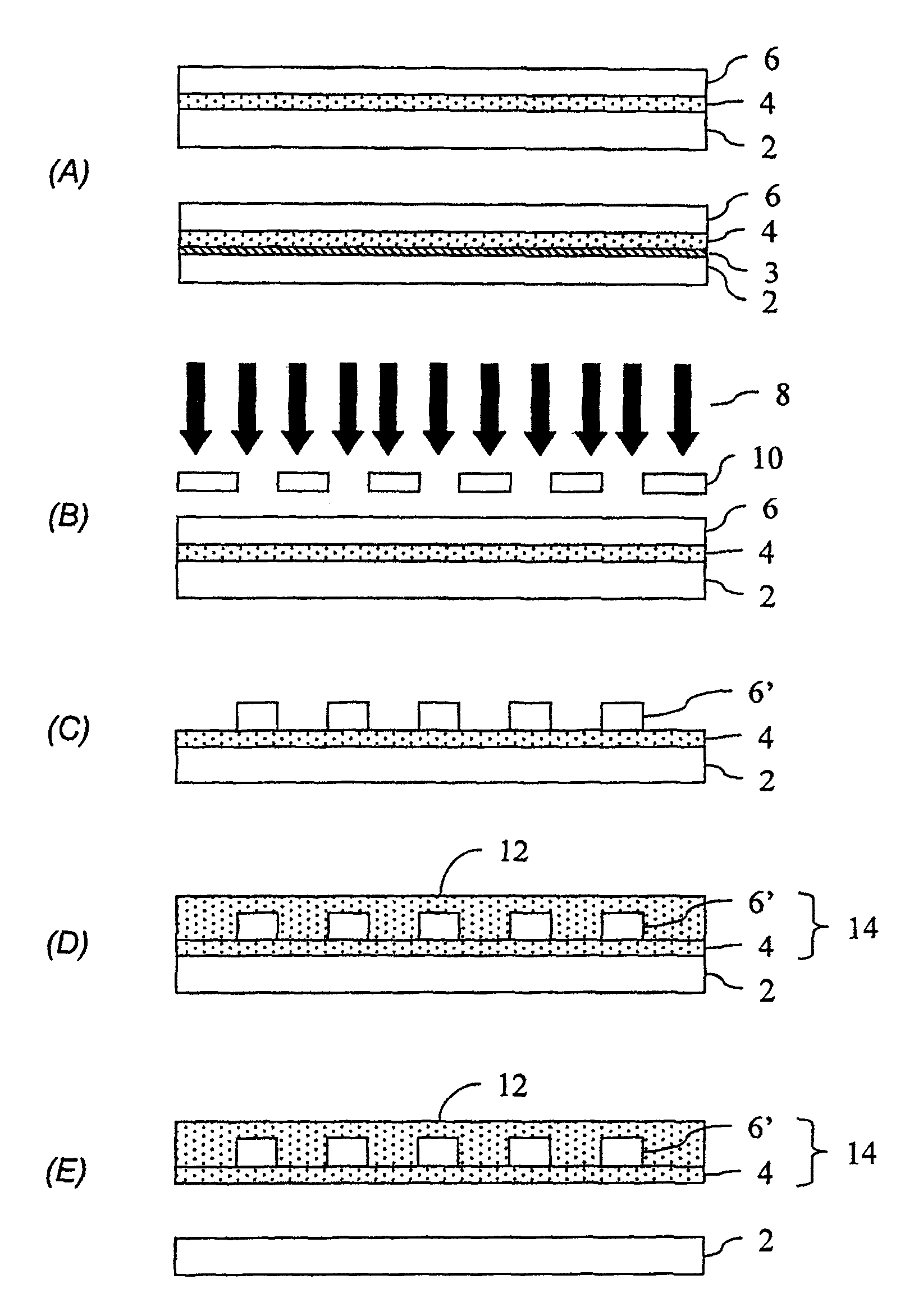
如图1A所示,提供要在其上形成光波导的基底2。选择基底材料,使得要形成的波导结构可与基底分离而不会损坏波导结构。通常,基底材料包括,例如玻璃、不锈钢、金属箔(如铜箔)、高冲击性聚苯乙烯等。任选地,可在基底上形成释放层3,该释放层可使波导结构与基底容易分离。用于任选的释放层的合适的材料包括,例如热固化或光化学固化的硅、聚硬脂酸乙烯酯、聚氨基甲酸乙烯酯、聚N-乙基-全氟乙酰基(actyl)磺酰氨基乙基(sulfanamidoethyl)甲基丙烯酸酯、以及其它释放材料,如描述在压敏粘合剂技术手册(第二版,Van Nostrand/Reinhold公司(1989))中的那些材料。任选地,所述基底可以是溶解释放出波导结构的牺牲材料,例如,用于酸性蚀刻剂的铜箔基底。As shown in FIG. 1A, a
然后,在基底2上形成波导结构。所述波导可通过,例如多层方法形成,该方法包括形成第一覆层,形成核层,随后使核图案化,以及形成第二覆层。另一种例举的工艺使用多光子吸附以将波导层的内容积暴露出来,从而导致暴露体积的折射率改变以形成波导,而无需用机械的方法使核层图案化。Then, a waveguide structure is formed on the
所述波导覆层和/或核是由含硅材料形成的。合适的含硅材料包括,例如倍半硅氧烷、笼状倍半硅氧烷、硅氧烷、玻璃如SOG或掺杂质的玻璃(例如,BPSG、PSG、BSG)、以及它们的组合。所述波导可由例如包含混合有机-无机聚合物的组合物形成,该聚合物具有由通式(RSiO1.5)表示的单元,式中R是取代或未取代的有机基团。该聚合物可具有许多官能端基。在所述组合物中聚合物的含量可以是1-99.5重量%,例如60-98.5重量%。例举的用于R的有机基团包括取代和未取代的烷基、芳基和杂环基。烷基可以是直链的、支链的或环状的,具有例如1-20个碳原子,通常具有1-20个碳原子,例如甲基、乙基、丙基、异丙基、叔丁基、叔戊基、辛基、癸基、十二烷基、十六烷基、硬脂酰、环己基和2-乙基己基。例如,所述烷基可被在烷基链中和/或链上的杂原子取代,或者可以是非芳香环状基团,如环戊基、环己基、降冰片烷基(norbonyl)、金刚烷基、哌啶基、四氢呋喃基和四氢苯硫基。例举的芳基包括具有6-20个碳原子,例如6-15个碳原子的那些基团,例如苯基、甲苯基、苄基、1-萘基、2-萘基和2-菲基,并且可被杂原子(例如羟基和/或氨基)取代。杂环基可以是芳香族的,例如,噻吩、吡啶、嘧啶、吡咯、磷醚(phosphole)、砷醚(arsole)和呋喃。通常,用于R的是取代和未取代的甲基、乙基、丙基、环戊基、环己基、苄基、苯基、金刚烷基、以及它们的组合。The waveguide cladding and/or core are formed from a silicon-containing material. Suitable silicon-containing materials include, for example, silsesquioxanes, cage silsesquioxanes, siloxanes, glasses such as SOG or doped glasses (eg, BPSG, PSG, BSG), and combinations thereof. The waveguide can be formed, for example, from a composition comprising a hybrid organic-inorganic polymer having units represented by the general formula (RSiO 1.5 ), where R is a substituted or unsubstituted organic group. The polymer can have many functional end groups. The content of the polymer in the composition may be 1-99.5% by weight, for example 60-98.5% by weight. Exemplary organic groups for R include substituted and unsubstituted alkyl, aryl and heterocyclyl groups. Alkyl can be linear, branched or cyclic, having for example 1-20 carbon atoms, usually 1-20 carbon atoms, e.g. methyl, ethyl, propyl, isopropyl, tert-butyl tert-amyl, octyl, decyl, dodecyl, hexadecyl, stearyl, cyclohexyl and 2-ethylhexyl. For example, the alkyl group may be substituted by heteroatoms in and/or on the alkyl chain, or may be a non-aromatic cyclic group such as cyclopentyl, cyclohexyl, norbonyl, adamantane group, piperidinyl, tetrahydrofuranyl and tetrahydrophenylthio. Exemplary aryl groups include those having 6-20 carbon atoms, such as 6-15 carbon atoms, such as phenyl, tolyl, benzyl, 1-naphthyl, 2-naphthyl and 2-phenanthrenyl , and may be substituted by heteroatoms such as hydroxyl and/or amino. The heterocyclic group can be aromatic, eg, thiophene, pyridine, pyrimidine, pyrrole, phosphole, arsole, and furan. Typically, for R are substituted and unsubstituted methyl, ethyl, propyl, cyclopentyl, cyclohexyl, benzyl, phenyl, adamantyl, and combinations thereof.
所述聚合物可呈共聚物或更高级的聚合物的形式,是无规的或是嵌段类型的。聚合物可包括,例如一个或多个附加的含硅单元,各个单元的比例为1-85重量%,例如15-80重量%、25-60重量%或25-50重量%,以聚合物计。所述附加的单元可由,例如倍半硅氧烷、笼状硅氧烷、硅氧烷、以及它们的组合来表示。例如,所述聚合物还可包括由通式(R1SiO1.5)表示的单元,式中R1是与上述R相同的取代或未取代的有机基团。R和R1中的一个可选自,例如取代或未取代的烷基,而R和R1中的另一个选自取代或未取代的芳基。所述聚合物可以是,例如,烷基硅聚合物,如含有甲基倍半硅氧烷单元和丁基倍半硅氧烷单元的共聚物;芳基硅聚合物,如含有苯基倍半硅氧烷单元和三氟甲苯基-倍半硅氧烷单元的共聚物;或者芳烷基硅共聚物,如含有甲基和苯基倍半硅氧烷单元的共聚物。The polymers may be in the form of copolymers or higher polymers, random or block type. The polymer may comprise, for example, one or more additional silicon-containing units in a proportion of 1-85% by weight, for example 15-80% by weight, 25-60% by weight or 25-50% by weight, based on the polymer . The additional units can be represented by, for example, silsesquioxanes, cage siloxanes, siloxanes, and combinations thereof. For example, the polymer may further include a unit represented by the general formula (R 1 SiO 1.5 ), where R 1 is the same substituted or unsubstituted organic group as R above. One of R and R may be selected, for example, from substituted or unsubstituted alkyl, while the other of R and R may be selected from substituted or unsubstituted aryl. The polymer can be, for example, an alkyl silicon polymer, such as a copolymer containing methylsilsesquioxane units and butylsilsesquioxane units; an aryl silicon polymer, such as a copolymer containing phenylsilsesquioxane units; Copolymers of siloxane units and trifluorocresyl-silsesquioxane units; or aralkylsilicone copolymers, such as copolymers containing methyl and phenylsilsesquioxane units.
合适的硅氧烷单元包括,例如由通式((R2)2SiO)表示的单元,式中R2是取代或未取代的有机基团如烷基,例如甲基、乙基、丙基等,或者芳基,例如苯基、甲苯基等。Suitable siloxane units include, for example, units represented by the general formula ((R 2 ) 2 SiO), where R 2 is a substituted or unsubstituted organic group such as an alkyl group, for example methyl, ethyl, propyl etc., or aryl groups such as phenyl, tolyl, etc.
如上所述,所述聚合物的侧链基团可任选地被取代。“取代”是指在一个或多个侧链基团上的一个或多个氢原子被另一个取代基所代替,所述取代基例如氘、卤素(如氟、溴和氯)、(C1-C6)烷基、(C1-C6)卤烷基、(C1-C10)烷氧基、(C1-C10)烷基羰基、(C1-C10)烷氧基羰基、(C1-C10)烷基羰氧基、烷基胺、含有烷基硫的材料等。所述聚合物可含有宽范围的重复单元,这些重复单元是无规的或嵌段的。用于本发明的聚合物单元可具有,例如5-150个重复单元,通常是约10-35个重复单元;用于本发明的硅氧烷单元可具有例如5-150个重复单元,通常是约7-25个重复单元。因此,所述聚合物的分子量差异很大。通常,所述聚合物的重均分子量(Mw)约为500-15,000,更一般的是约1000-10,000,再一般的是1000-5000。As noted above, the side chain groups of the polymer may be optionally substituted. "Substitution" means that one or more hydrogen atoms on one or more side chain groups are replaced by another substituent, such as deuterium, halogen (such as fluorine, bromine and chlorine), (C 1 -C 6 )alkyl, (C 1 -C 6 )haloalkyl, (C 1 -C 10 )alkoxy, (C 1 -C 10 )alkylcarbonyl, (C 1 -C 10 )alkoxy Carbonyl, (C 1 -C 10 )alkylcarbonyloxy, alkylamine, alkylsulfide-containing materials, and the like. The polymers may contain a wide range of repeat units, either random or block. The polymer units used in the present invention can have, for example, 5-150 repeating units, usually about 10-35 repeating units; the siloxane units used in the present invention can have, for example, 5-150 repeating units, usually about About 7-25 repeat units. Accordingly, the molecular weights of the polymers vary widely. Typically, the polymer has a weight average molecular weight ( Mw ) of about 500-15,000, more typically about 1000-10,000, and still more typically 1000-5000.
所述聚合物可包括两个或多个官能端基,所述端基使得组合物在光活化之后溶解性改变。所述端基可以是,例如羟基;烷氧基,如乙氧基、丙氧基、异丙氧基;羧基酯、氨基、酰氨基、环氧基、亚氨基、羧酸、酸酐、烯基、丙烯酸、乙缩醛、原酸酯、乙烯基醚、以及它们的组合。所述官能端基的含量可以是,例如约0.5-35重量%,如约1-10重量%,或者约2-5重量%,以聚合物计。The polymer may include two or more functional end groups that allow the composition to undergo a change in solubility upon photoactivation. The terminal group may be, for example, hydroxyl; alkoxy, such as ethoxy, propoxy, isopropoxy; carboxyl ester, amino, amido, epoxy, imino, carboxylic acid, anhydride, alkenyl , acrylic acid, acetal, ortho ester, vinyl ether, and combinations thereof. The functional end groups may be present, for example, in an amount of about 0.5-35% by weight, such as about 1-10% by weight, or about 2-5% by weight, based on the polymer.
该组合物还可含有光敏成分。通常,所述光敏成分在活化时会产生酸或碱,并在显影剂中改变呈干燥状态的组合物的溶解性。本发明可使用多种光敏成分,包括,但不限于光酸产生剂和光碱产生剂。The composition may also contain a photosensitive ingredient. Typically, the photosensitive components generate acids or bases upon activation and alter the solubility of the composition in the dry state in the developer. A variety of photosensitive components can be used in the present invention, including, but not limited to, photoacid generators and photobase generators.
适用于本发明的光酸产生剂可以是当暴露在光照下能够产酸的任何化合物。合适的光酸产生剂是已知的,包括,但不限于卤代三嗪、鎓盐、磺酸酯、取代的羟基酰亚胺、取代羟基亚胺、叠氮化物、萘醌(如重氮萘醌)、重氮化合物、以及它们的组合。Photoacid generators suitable for use in the present invention can be any compound capable of generating acid when exposed to light. Suitable photoacid generators are known and include, but are not limited to, halotriazines, onium salts, sulfonates, substituted hydroxyimides, substituted hydroxyimides, azides, naphthoquinones (such as diazo naphthoquinone), diazo compounds, and combinations thereof.
特别有用的卤代三嗪包括,例如卤代烷基三嗪,如三卤甲基-仲三嗪。仲三嗪化合物是特定的甲基-三卤甲基-仲三嗪与特定的醛或醛衍生物的缩合反应产物。所述仲三嗪化合物可根据美国专利3,954,475和Wakabayashi等的日本化学协 会公报(42,2924-30(1969))中公开的方法来制备。其它适用于本发明的三嗪类光酸产生剂公开在例如美国专利5,366,846中。Particularly useful halotriazines include, for example, haloalkyltriazines such as trihalomethyl-secondary triazines. Secondary triazine compounds are condensation reaction products of specific methyl-trihalomethyl-secondary triazines with specific aldehydes or aldehyde derivatives. The secondary triazine compound can be prepared according to the methods disclosed in US Pat. No. 3,954,475 and the Bulletin of the Chemical Society of Japan by Wakabayashi et al. (42, 2924-30 (1969)). Other triazine photoacid generators suitable for use in the present invention are disclosed, for example, in US Patent No. 5,366,846.
含有弱亲核性阴离子的鎓盐特别适合用作本发明的光酸产生剂。所述阴离子的例子有二价至七价金属或非金属的卤素络合物阴离子,所述金属或非金属例如锑、锡、铁、铋、铝、镓、铟、钛、锆、钪、铬、铪、铜、硼、磷和砷。合适的鎓盐的例子包括,但不限于,重氮盐如二芳基-重氮盐,以及元素周期表第VA和VB、IIA和IIB、以及I族的鎓盐,例如卤鎓盐(如碘鎓盐、季铵盐、鏻盐和胂鉮盐),锍盐(如芳香锍盐、氧化锍盐或硒盐)。合适的鎓盐的例子公开在,例如美国专利4,442,197、4,603,101和4,624,912中。通常,使用锍盐如六氟磷酸三苯基锍,以及它们的混合物。Onium salts containing weakly nucleophilic anions are particularly suitable for use as photoacid generators in the present invention. Examples of said anions are halide complex anions of divalent to heptavalent metals or nonmetals such as antimony, tin, iron, bismuth, aluminum, gallium, indium, titanium, zirconium, scandium, chromium , hafnium, copper, boron, phosphorus and arsenic. Examples of suitable onium salts include, but are not limited to, diazonium salts such as diaryl-diazonium salts, and onium salts of Groups VA and VB, IIA and IIB, and Group I of the Periodic Table of the Elements, such as halonium salts (such as iodonium salts, quaternary ammonium salts, phosphonium salts and arsenic salts), sulfonium salts (such as aromatic sulfonium salts, sulfoxonium salts or selenium salts). Examples of suitable onium salts are disclosed, for example, in US Patent Nos. 4,442,197, 4,603,101 and 4,624,912. Typically, sulfonium salts such as triphenylsulfonium hexafluorophosphate, and mixtures thereof are used.
适合用作本发明的光酸产生剂的磺酸酯包括,例如磺酰氧基酮。合适的磺酸酯包括,但不限于苯偶姻甲苯磺酸酯、α-(对甲苯磺酰氧基)-醋酸叔丁基苯酯、甲苯磺酸2,6-二硝基苯酯和α-(对甲苯磺酰氧基)-醋酸叔丁酯。所述磺酸酯公开在,例如光敏聚合物科学和技术杂志(第4卷,3,337-340(1991))中。Sulfonate esters suitable for use as photoacid generators in the present invention include, for example, sulfonyloxyketones. Suitable sulfonates include, but are not limited to, benzoin tosylate, α-(p-toluenesulfonyloxy)-tert-butylphenyl acetate, 2,6-dinitrophenyl toluenesulfonate, and α -(p-Toluenesulfonyloxy)-tert-butyl acetate. Such sulfonates are disclosed, for example, in Journal of Photopolymer Science and Technology (Vol. 4, 3, 337-340 (1991)).
可以使用的取代的羟基酰亚胺包括,例如正三氟甲基磺酰氧基-2,3-二苯基马来酰亚胺和2-三氟甲基苯磺酰氧基-2,3-二苯基马来酰亚胺。合适的取代的羟基亚胺包括,例如2-(次氮基-2-甲基苯亚甲基)-(5-羟基亚氨基丁基磺酰基)-噻吩。适用于本发明的叠氮化物包括,例如2,6-(4-叠氮基苯亚甲基)环己酮。萘醌可包括,例如2,3,4-三羟基二苯甲酮的2,1-叠氮基萘醌-4-磺酸酯。在重氮化合物中,可以使用1,7-二(4-氯磺酰基苯基)-4-重氮基-3,5-庚二酮。Substituted hydroxyimides that can be used include, for example, n-trifluoromethylsulfonyloxy-2,3-diphenylmaleimide and 2-trifluoromethylbenzenesulfonyloxy-2,3- Diphenylmaleimide. Suitable substituted hydroxyimines include, for example, 2-(nitrilo-2-methylbenzylidene)-(5-hydroxyiminobutylsulfonyl)-thiophene. Azides suitable for use in the present invention include, for example, 2,6-(4-azidobenzylidene)cyclohexanone. Naphthoquinones may include, for example, 2,1-azidonaphthoquinone-4-sulfonate of 2,3,4-trihydroxybenzophenone. Among the diazo compounds, 1,7-bis(4-chlorosulfonylphenyl)-4-diazo-3,5-heptanedione can be used.
适用于本发明的光碱产生剂可以是在暴露于光照下释放出碱的任何化合物。合适的光碱产生剂包括,但不限于氨基甲酸苄酯、苯偶姻氨基甲酸酯、O-氨基甲酰羟基胺、O-氨基甲酰肟、芳香磺酰胺、α-内酰胺、N-(2-烯丙基乙烯基)酰氨、芳基叠氮化合物、N-芳基甲酰胺、4-(邻硝基苯基)二氢吡啶、以及它们的组合。Photobase generators suitable for use in the present invention can be any compound that releases a base upon exposure to light. Suitable photobase generators include, but are not limited to, benzyl carbamate, benzoin carbamate, O-carbamoyl hydroxylamine, O-carbamoyl oxime, aromatic sulfonamide, α-lactam, N- (2-allylvinyl) amides, aryl azides, N-aryl formamides, 4-(o-nitrophenyl) dihydropyridines, and combinations thereof.
在使用负加工材料的情况下,适用于本发明的用于改变溶解性的光敏成分的量是在暴露于光化辐射下时足以改变组合物的溶解性并使曝光部分不溶于显影剂中的任何量。通常,光敏成分的量为0.1-25重量%,例如0.1-12重量%,以组合物计。In the case of negative processing materials, the amount of the solubility-altering photosensitive ingredient suitable for use in the present invention is sufficient to alter the solubility of the composition and render the exposed portions insoluble in the developer upon exposure to actinic radiation. any amount. Typically, the photoactive ingredient is present in an amount of 0.1-25% by weight, such as 0.1-12% by weight, based on the composition.
所述组合物中可以存在一种或多种用以改善由组合物形成的结构的挠性的成分。这些挠性改善材料通常包含许多官能团,所述光能团选自羟基、氨基、硫醇、磺酸酯、羧酸酯、甲硅烷酯、酸酐、氮丙啶、羟甲基甲基、甲硅烷酯、环氧化物、氧杂环丁烷、乙烯基醚、硅烷醇、以及它们的组合。在挠性改善材料中,光能团通常附着在主链材料上。例举的主链材料包括取代和未取代的烷烃和芳香烃、醚、丙烯酸酯、酚醛清漆、聚酰亚胺、聚氨酯、聚酯、聚砜、聚酮、呋仑碳(fullerenes)、POSS硅、纳米颗粒、以及它们的组合。所述光能团可作为端基存在于主链和/或沿主链的一个或多个位置上。One or more ingredients may be present in the composition to improve the flexibility of structures formed from the composition. These flexibility-improving materials generally contain many functional groups selected from the group consisting of hydroxyl, amino, thiol, sulfonate, carboxylate, silyl ester, anhydride, aziridine, hydroxymethylmethyl, silane Esters, epoxides, oxetanes, vinyl ethers, silanols, and combinations thereof. In flexibility-improving materials, photon groups are usually attached to the main chain material. Exemplary backbone materials include substituted and unsubstituted alkanes and aromatics, ethers, acrylates, novolacs, polyimides, polyurethanes, polyesters, polysulfones, polyketones, fullerenes, POSS silicon , nanoparticles, and combinations thereof. The photophores may be present as end groups on the backbone and/or at one or more positions along the backbone.
挠性成分的例子有由通式R3(OH)x表示的多元醇,式中R3是有机基团,选自取代或未取代的(C2-C25)烷基、(C7-C25)芳基、(C8-C25)芳烷基、(C6-C25)环烷基、以及它们的组合,式中x为2或更大的数字,但不超过碳原子的数目。当x是2时,挠性成分的例子包括二醇,它是1,2-二醇,例如HOCH2-CHOH-(CH2)y-CH3,式中y可以是,例如0-22,如丙二醇和丁二醇。其它例子包括α,ω-二醇,如HO-(CH2)z-OH,式中z是,例如2-25,如乙二醇、1,3-丙二醇和1,4-丁二醇。当x是3时,例子包括丙三醇和三羟甲基丙烷。Examples of flexible components are polyols represented by the general formula R 3 (OH) x , where R 3 is an organic group selected from substituted or unsubstituted (C 2 -C 25 )alkyl, (C 7 - C 25 ) aryl, (C 8 -C 25 ) aralkyl, (C 6 -C 25 ) cycloalkyl, and combinations thereof, where x is a number of 2 or more, but not exceeding the number of carbon atoms number. When x is 2, examples of flexible components include diols, which are 1,2-diols such as HOCH 2 -CHOH-(CH 2 ) y -CH 3 , where y can be, for example, 0-22, Such as propylene glycol and butylene glycol. Other examples include α,ω-diols, such as HO-(CH 2 ) z -OH, where z is, for example, 2-25, such as ethylene glycol, 1,3-propanediol and 1,4-butanediol. When x is 3, examples include glycerol and trimethylolpropane.
R3也可以是由通式-O-(CR4 2)w-表示的聚醚,式中w是,例如1-13,R4可以相同或不同,可以是,例如H,或者通式C1-C12烷基、芳基、芳烷基或环烷基的取代或未取代的有机基团。挠性成分的例子包括聚环氧乙烷、聚环氧丙烷、聚环氧丁烷和聚四氢呋喃的聚醚二醇。R 3 can also be a polyether represented by the general formula -O-(CR 4 2 ) w -, where w is, for example, 1-13, and R 4 can be the same or different, and can be, for example, H, or the general formula C A substituted or unsubstituted organic group of 1 -C 12 alkyl, aryl, aralkyl or cycloalkyl. Examples of flexible components include polyether glycols of polyethylene oxide, polypropylene oxide, polybutylene oxide, and polytetrahydrofuran.
挠性改善成分的重均分子量可以是,例如62-5000,如62-2000。该成分以有效量存在以改善活化前后呈干燥状态的组合物的挠性。具体的用量取决于,例如挠性改善成分的主链及其官能团的种类和数量。该成分的量可以是,例如0.5-35重量%,如2-20重量%,以组合物计。The weight average molecular weight of the flexibility improving component may be, for example, 62-5000, such as 62-2000. This ingredient is present in an effective amount to improve the flexibility of the composition in the dry state before and after activation. The specific amount depends, for example, on the main chain of the flexibility-improving component and the type and amount of its functional groups. The amount of this ingredient may be, for example, 0.5-35% by weight, such as 2-20% by weight, based on the composition.
除了上述增韧剂以外,也可以使用硅氧烷,例如上述具有由通式((R2)2SiO)表示的单元的那些。In addition to the aforementioned toughening agents, siloxanes such as those described above having units represented by the general formula ((R 2 ) 2 SiO) may also be used.
其它添加剂也可任选地存在于所述组合物中,包括,但不限于表面流平剂、湿润剂、消泡剂、促粘剂、触变剂、填充剂、粘度调节剂等。这些添加剂是涂料组合物领域所熟知的。可以在组合物中使用表面流平剂,例如硅酮系油,如购自Dow Chemical公司的SILWET L-7604硅酮系油。可以明白,可在本发明的组合物中结合使用超过一种的添加剂。例如,可以将湿润剂和触变剂结合。这些用于本发明的任选的添加剂的量取决于具体的添加剂和所需的效果,并且在本领域普通技术人员的能力范围内。这些其它添加剂的用量通常小于5重量%,例如小于2.5重量%,以组合物计。Other additives may also optionally be present in the composition, including, but not limited to, surface leveling agents, wetting agents, defoamers, adhesion promoters, thixotropic agents, fillers, viscosity modifiers, and the like. These additives are well known in the art of coating compositions. Surface leveling agents, such as silicone based oils such as SILWET L-7604 silicone based oil available from Dow Chemical Company, can be used in the composition. It will be appreciated that more than one additive may be used in combination in the compositions of the present invention. For example, wetting agents and thixotropic agents can be combined. The amounts of these optional additives used in the present invention depend on the particular additive and the desired effect and are within the purview of one of ordinary skill in the art. These other additives are typically used in amounts of less than 5% by weight, such as less than 2.5% by weight, based on the composition.
适用于本发明方法的组合物可任选地含有一种或多种有机交联剂。所述交联剂包括,例如以三维方式连接所述组合物的成分的材料。与含硅聚合物反应的芳族或脂族交联剂适用于本发明。所述有机交联剂将固化以与含硅聚合物形成聚合网络,并降低在显影剂溶液中的溶解性。所述有机交联剂可以是单体或聚合物。本领域的技术人员将会明白,在本发明中也可以成功地使用交联剂的组合。Compositions suitable for use in the methods of the present invention may optionally contain one or more organic crosslinking agents. The crosslinking agent includes, for example, a material that links the components of the composition in a three-dimensional manner. Aromatic or aliphatic crosslinkers reactive with silicon-containing polymers are suitable for use in the present invention. The organic crosslinker will cure to form a polymeric network with the silicon-containing polymer and reduce solubility in developer solutions. The organic crosslinking agent can be a monomer or a polymer. Those skilled in the art will appreciate that combinations of crosslinking agents can also be used successfully in the present invention.
用于本发明的合适的有机交联剂包括,但不限于含胺化合物、含环氧树脂的材料、含至少两个乙烯基醚基团的化合物、烯丙基取代的芳香化合物、以及它们的组合。一般的的交联剂包括含胺化合物和含环氧树脂的材料。Suitable organic crosslinking agents for use in the present invention include, but are not limited to, amine-containing compounds, epoxy-containing materials, compounds containing at least two vinyl ether groups, allyl-substituted aromatic compounds, and combinations thereof combination. Typical crosslinking agents include amine-containing compounds and epoxy-containing materials.
适合用作本发明的交联剂的含胺化合物包括,但不限于三聚氰胺单体、三聚氰胺聚合物、羟烷基甲基三聚氰胺、苯并胍胺树脂、苯并胍胺-甲醛树脂、脲-甲醛树脂、甘脲-甲醛树脂、以及它们的组合。Amine-containing compounds suitable for use as crosslinking agents in the present invention include, but are not limited to, melamine monomers, melamine polymers, hydroxyalkylmethylmelamines, benzoguanamine resins, benzoguanamine-formaldehyde resins, urea-formaldehyde Resins, glycoluril-formaldehyde resins, and combinations thereof.
本领域技术人员将会明白,合适的有机交联剂的浓度将根据各种因素如交联剂的反应性和组合物的具体应用而变化。在使用时,交联剂的量通常为0.1-50重量%,例如0.5-25重量%或1-20重量%。Those skilled in the art will appreciate that the concentration of a suitable organic crosslinker will vary depending on factors such as the reactivity of the crosslinker and the particular application of the composition. When used, the amount of crosslinking agent is generally 0.1-50% by weight, such as 0.5-25% by weight or 1-20% by weight.
所述组合物可任选地含有一种或多种溶剂。所述溶剂有助于配制组合物并将组合物涂覆在基底上。可以使用的溶剂种类繁多。合适的溶剂包括,但不限于二醇醚(如乙二醇单甲醚、丙二醇单甲醚和二丙二醇单甲醚),酯(如甲基乙酸溶纤剂、乙基乙酸溶纤剂、丙二醇一甲醚醋酸酯、二丙二醇一甲醚醋酸酯、二价酸酯、碳酸酯如碳酸亚丙酯、γ-丁内酯),酯(如乳酸乙酯、醋酸正戊酯和醋酸正丁酯),醇(如正丙醇、异丙醇),酮(如环己酮、甲基异丁基酮、二异丁基酮和2-庚酮),内酯(如γ-丁内酯和γ-己内酯),醚(如二苯醚和苯甲醚),烃(如均三甲基苯、甲苯和二甲苯),以及杂环化合物(如N-甲基-2-吡咯烷酮和N,N’-二甲基亚丙基脲),或者它们的混合物。The composition may optionally contain one or more solvents. The solvent aids in formulating the composition and applying the composition to the substrate. A wide variety of solvents can be used. Suitable solvents include, but are not limited to, glycol ethers (such as ethylene glycol monomethyl ether, propylene glycol monomethyl ether, and dipropylene glycol monomethyl ether), esters (such as methyl acetate cellosolve, ethyl acetate cellosolve, propylene glycol Monomethyl ether acetate, dipropylene glycol monomethyl ether acetate, dibasic esters, carbonates such as propylene carbonate, gamma-butyrolactone), esters (such as ethyl lactate, n-pentyl acetate and n-butyl acetate ), alcohols (such as n-propanol, isopropanol), ketones (such as cyclohexanone, methyl isobutyl ketone, diisobutyl ketone and 2-heptanone), lactones (such as γ-butyrolactone and γ-caprolactone), ethers (such as diphenyl ether and anisole), hydrocarbons (such as mesitylene, toluene, and xylene), and heterocyclic compounds (such as N-methyl-2-pyrrolidone and N , N'-dimethylpropylene urea), or a mixture thereof.
所述组合物可通过以混合物的形式,以任意次序结合含硅聚合物和其它任选的成分来制备。The composition can be prepared by combining the silicon-containing polymer and other optional ingredients in admixture, in any order.
所述聚合层可以通过各种工艺来形成,这些工艺包括,但不限于丝网印刷、幕涂、辊涂、槽涂、旋涂、泛涂、静电喷雾、喷涂或浸涂。当喷涂所述组合物时,可任选地使用加热的喷雾枪。可以用粘度调节剂、触变剂、填充剂等调节组合物的粘度,以使其满足各种应用方法的要求。层的厚度取决于具体的应用。然而,在干燥状态下的厚度通常为1-100μm,例如约10-50μm。The polymeric layer can be formed by various processes including, but not limited to, screen printing, curtain coating, roll coating, slot coating, spin coating, flood coating, electrostatic spraying, spray coating, or dip coating. When spraying the composition, a heated spray gun may optionally be used. Viscosity modifiers, thixotropic agents, fillers, etc. can be used to adjust the viscosity of the composition to meet the requirements of various application methods. The thickness of the layers depends on the specific application. However, the thickness in a dry state is generally 1-100 μm, for example about 10-50 μm.
然后,通常对涂覆的基底进行干燥以基本上从涂层上除去溶剂。干燥可在,例如炉(如红外线炉、对流炉、对流/传导炉、真空炉),或者加热板上进行。所述干燥可在各种温度和时间下进行,取决于所选择的具体溶剂和干燥工艺。合适的温度是足以基本上除去存在的溶剂的任何温度。通常,干燥可以在室温(25℃)-170℃之间的任何温度,以及5秒钟-120分钟之间的时间下进行。当使用炉时,一般的时间是10-120分钟,对于加热板是10秒钟-10分钟。The coated substrate is then typically dried to substantially remove the solvent from the coating. Drying can be performed, for example, in an oven (eg, infrared oven, convection oven, convection/conduction oven, vacuum oven), or on a hot plate. The drying can be performed at various temperatures and times, depending on the specific solvent and drying process chosen. A suitable temperature is any temperature sufficient to substantially remove the solvent present. In general, drying can be performed at any temperature between room temperature (25°C) and 170°C, and for a time between 5 seconds and 120 minutes. Typical times are 10-120 minutes when using an oven, and 10 seconds-10 minutes for a hot plate.
第一覆层4形成在基底2(具有或不具有释放层3),核层6形成在第一覆层4上。在使用可光学成像的核材料的情况下,例如通过使核层6透过光掩膜10暴露在光化辐射8下(如图1B所示)使其成像。如图1C所示,核层6的未曝光的部分通过显影除去,剩下一个或多个核结构6’。可以用其它工艺,例如使用标准的光蚀刻和蚀刻工艺使核层6图案化。在这种情况下,可将光致抗蚀剂涂覆在波导核层上并通过含有所需图案的原图曝光。曝光的区域(在使用正光致抗蚀剂的情况下)或未曝光的区域(使用负光致抗蚀剂的情况下)在显影剂中被洗去。该图案则通过蚀刻(如反应离子蚀刻)而转移至波导核上,并除去光致抗蚀剂。在形成核结构6’之后,在第一覆层4和核结构6’上形成第二覆层12,如图1D所示。由此形成包括第一覆层4、核层6和第二覆层12的波导结构14。The
可分别选择用于第一覆层、核和第二覆层的材料,只是要明白最终的核结构的折射率应当高于覆层的折射率。这些层的厚度可以在5-500μm,例如通常是8-50μm的宽范围内变动。对于单模式应用,厚度通常为6-10μm,而对于多模式应用,厚度通常为40-60μm。The materials for the first cladding, core and second cladding can be chosen separately, just with the understanding that the refractive index of the final core structure should be higher than that of the cladding. The thickness of these layers can vary within a wide range of 5-500 μm, for example typically 8-50 μm. For single-mode applications, the thickness is typically 6-10 μm, while for multi-mode applications, the thickness is typically 40-60 μm.
如图1E所示,接着使波导结构14与基底2分离。这可通过,例如在使用玻璃基底和倍半硅氧烷系波导的情况下,将图1D所示的结构浸在加热的去离子水浴中来完成,所述去离子水浴的温度和浸泡的时间足以使波导结构14与基底2分离。尽管所使用的温度和时间取决于具体的波导和使用的基底材料,然而水温通常为30-100℃,时间通常为60-120分钟。在分离以后,从水浴中取出波导结构,并通过在110℃的炉中加热15分钟对其进行干燥以除去任何存留的液体。As shown in FIG. 1E , the
基底的去除也可以通过蚀刻(例如在使用铜箔基底的情况下)完成。合适的蚀刻剂包括,例如1%的盐酸、1%的硫酸、氯化铜和硫过氧化物。Removal of the substrate can also be accomplished by etching (for example in the case of a copper foil substrate). Suitable etchants include, for example, 1% hydrochloric acid, 1% sulfuric acid, copper chloride, and sulfur peroxide.
在基底2与波导结构14之间使用释放层的情况下,要根据波导覆层和释放层的材料来选择分离工艺。对某些释放层,例如聚对苯二甲酸乙二酯、热固化或光化学固化的硅释放层、聚(四氟乙烯)、聚丙烯、聚甲基丙烯酸甲酯、聚硅氧烷和聚酰胺的分离,可以简单地通过将波导从释放层和基底上剥离来完成,不需要使用液体介质。如果单独的释放层就足以机械地支持波导结构的处理,可使用它作为基底。通常,可以使用任何能够耐受处理条件并且可以在处理完成时轻易地从其上去除波导材料的基底。In case a release layer is used between the
上述参照图1的波导形成和分离方法或者至分离步骤之前的方法,可有利地在干净的环境(例如,级别为1000或更干净的环境,它与制造印刷电路板基底所处的微粒环境隔离)中进行。结果,可将对波导性能的与污染物相关的影响(如光学特性的丧失和图案缺陷)减至最小或者消除。然后,将形成的波导结构置于印刷电路板制造区中用于印刷电路板的装配。The waveguide formation and separation method described above with reference to FIG. 1, or the method up to the separation step, may advantageously be performed in a clean environment (e.g., a class 1000 or better environment that is isolated from the particulate environment in which the printed circuit board substrate is manufactured. ) in. As a result, contamination-related effects on waveguide performance, such as loss of optical properties and pattern defects, can be minimized or eliminated. The formed waveguide structure is then placed in a printed circuit board fabrication area for printed circuit board assembly.
如图2A所示,提供印刷电路板基底18。通常,印刷电路板基底是含有一系列环氧树脂和铜层的层压板,其上形成了蚀刻电路,导电线路和电子元件,或者它们将形成在一面或两个面上。As shown in FIG. 2A, a printed
将上述波导结构14与印刷电路板18接触并粘附在其上,如图2C所示。在此之前,可先在波导结构14和印刷电路板18的接触面中的一个或者两个面上施加粘合材料20,例如环氧树脂、丙烯酸、硅酮、橡胶、ABS、苯乙烯/丁二烯、聚异丁烯、聚异戊二烯等,如图2B所示。根据所使用的粘合剂,可以进行进一步处理,例如热固化、光固化或干燥以除去溶剂。可以使用其它工艺(例如,加热加压层压),或者使用部分固化的粘性第二覆层并使用第二覆层作为粘合剂层将波导结构粘附到基底上,将两个结构粘附起来。The above-mentioned
在将波导结构14粘附到印刷电路板基底18上以后,可以对印刷电路板做进一步处理。例如,可以在波导结构14上形成一层或多层介电层和/或金属层,以形成用于信号通路的敷金属结构。也可以在该阶段进行光电器件(如光电探测器或激光发射装置(例如,VCSEL芯片))的电连接。使用已知的工艺如描述在印刷电路手册(第五版,McGraw-Hill公司(2001))中的那些加工印刷电路板直至完成。After the
以下,将参照其余附图描述本发明的其它例举的实施方式。除非特别指出,上文的描述也适用于其它列举的方面。Hereinafter, other exemplary embodiments of the present invention will be described with reference to the remaining drawings. Unless otherwise specified, the above description is also applicable to other enumerated aspects.
图3示出了本发明的另一种例举的方法。该方法与图1所述方法的不同之处在于波导结构14仅部分地形成。所述波导结构包括用上文所述方法形成的第一覆层4和波导核结构6’。在形成第一覆层4和核6’之后,使波导结构14与基底2分离。参看图4A,在印刷电路板基底18的表面上形成第二覆层12。在该实施方式中,所述第二覆层12具有的粘度应当能使波导结构14的核结构6’在加压下插入其中。这可通过部分地干燥第二覆层材料来完成。使用面对电路板基底18和第二覆层12的核,使核结构6’与第二覆层12接触,并对其进行按压(例如层压)使其嵌入第二覆层12中,如图4B所示。可通过加热完成对第二覆层的固化。Figure 3 illustrates another exemplary method of the present invention. This method differs from the method described in FIG. 1 in that the
图5和6示出了本发明的另一个例举的方面,其中核结构6’首先形成于基底上,覆层12形成于基底2和核结构6’上,如图5A-B所示。使波导结构14与基底分离,如图5C所示。参看图6A,在印刷电路板基底上形成覆层4。使用面向电路板基底18和覆层4的核的曝光部分,使波导结构14与印刷电路板上的覆层4接触,如图6B所示。可通过诸如在加热和加压下层压的方式来将波导结构14粘附到覆层4上。Figures 5 and 6 illustrate another exemplary aspect of the invention, wherein the core structure 6' is first formed on the substrate, and the
尽管前述例举的实施方式表明光波导结构粘附到印刷电路板基底的一个表面上,但是应当清楚的是可以在基底的相同面和/或相对面上粘附多个波导结构。图7示出了在基底的相对面装有光波导14的印刷电路板18。这一结构使得光学连接器的密度增加。Although the foregoing exemplary embodiments show optical waveguide structures adhered to one surface of a printed circuit board substrate, it should be clear that multiple waveguide structures may be adhered to the same and/or opposing surfaces of the substrate. Figure 7 shows a printed
下述预示性的实施例用于进一步描述本发明的各个方面,无论如何不是限制本发明的范围。The following prophetic examples serve to further describe various aspects of the invention and in no way limit the scope of the invention.
实施例Example
实施例1Example 1
A.波导的形成 A. Waveguide Formation
覆层(1)的形成Formation of cladding (1)
第一覆层组合物通过以混合物的形式混合以下物质形成:39.8重量%的丙二醇单甲醚醋酸酯、49.99重量%的苯-甲基倍半硅氧烷(50∶50)、10重量%的聚四氢呋喃、0.2重量%的胺嵌段对甲苯磺酸和0.01重量%的Dow SILWET L-7604硅酮系油。将所述组合物辊涂于玻璃基底上,并在90℃的强制通风炉中软烘焙15分钟至厚度为15μm,然后在180℃的强制通风炉中硬烘焙60分钟。The first coating composition is formed by mixing the following materials in the form of a mixture: 39.8% by weight of propylene glycol monomethyl ether acetate, 49.99% by weight of phenyl-methylsilsesquioxane (50:50), 10% by weight of Polytetrahydrofuran, 0.2% by weight of amine-blocked p-toluenesulfonic acid, and 0.01% by weight of Dow SILWET L-7604 silicone-based oil. The composition was roll coated on a glass substrate and soft baked in a forced air oven at 90°C for 15 minutes to a thickness of 15 μm, then hard baked in a forced air oven at 180°C for 60 minutes.
核的形成nuclei formation
核层组合物通过以混合物的形式混合以下物质形成:45重量%的丙二醇单甲醚醋酸酯、49重量%的苯基-甲基倍半硅氧烷(50∶50)、5重量%的聚二苯基硅氧烷、0.99重量%的三苯锍六氟磷酸酯和0.01重量%的Dow SILWET L-7604硅酮系油。将所述组合物辊压于第一覆层上,并在90℃的强制通风炉中软烘焙10分钟至厚度为50μm。将限定核结构的原图直接放置在核层上。该原图包括用于形成各种尺寸和形状的波导(如直线、分支和弯曲形状的波导,其长度在2-14cm之间,宽度在25-75μm之间)的图案。以800mJ/cm2的剂量对该结构物施加光化学辐射,随后在90℃的强制通风炉中进行后曝光烘焙15分钟。将曝光后的基底浸在0.7N的氢氧化钠显影剂溶液中,在38℃下维持2分钟。用去离子水淋洗基底并干燥。将这些层放置在180℃的强制通风炉中烘焙60分钟。The core layer composition was formed by mixing the following in a mixture: 45% by weight propylene glycol monomethyl ether acetate, 49% by weight phenyl-methylsilsesquioxane (50:50), 5% by weight poly Diphenylsiloxane, 0.99% by weight of triphenylsulfonium hexafluorophosphate, and 0.01% by weight of Dow SILWET L-7604 silicone-based oil. The composition was rolled onto the first coating and soft baked in a forced air oven at 90° C. for 10 minutes to a thickness of 50 μm. Place the original map defining the nuclear structure directly on the nuclear layer. The artwork includes patterns for forming waveguides of various sizes and shapes, such as straight, branched, and curved waveguides with lengths between 2-14 cm and widths between 25-75 μm. Actinic radiation was applied to the structure at a dose of 800 mJ/cm 2 , followed by a post-exposure bake in a forced-air oven at 90° C. for 15 minutes. The exposed substrate was immersed in a 0.7N sodium hydroxide developer solution at 38°C for 2 minutes. The substrate was rinsed with deionized water and dried. The layers were baked in a forced air oven at 180°C for 60 minutes.
覆层(2)的形成Formation of cladding (2)
在核结构和第一覆层上形成第二覆层,形成其的组合物和步骤与形成第一覆层的相同,除了软烘焙后第二覆层的厚度为70μm以外。由此形成光波导。A second cladding layer was formed on the core structure and the first cladding layer with the same composition and steps as those for forming the first cladding layer, except that the thickness of the second cladding layer was 70 μm after soft baking. Thus an optical waveguide is formed.
波导的分离waveguide separation
将基底浸在99℃的去离子水浴中30分钟,使波导结构与基底分离。从浴中取出波导结构,置于95℃的炉中干燥30分钟。The waveguide structure was separated from the substrate by immersing the substrate in a deionized water bath at 99°C for 30 minutes. The waveguide structure was removed from the bath and placed in an oven at 95°C for 30 minutes to dry.
B.印刷电路板的形成 B. Printed Circuit Board Formation
提供了具有两层铜电路内层和两层印刷电路外层的多层铜制电路板,该电路板通过标准层压法(包括使用环氧树脂预胎成层并进行层压)制备。所述电路板在其表面上有一个要粘合波导结构的区域。在电路板的粘合区上涂覆硅酮粘合剂。将波导结构按压到粘合剂上,并在50℃固化粘合剂30分钟。钻出贯穿波导和电路板的通孔。将铜镀敷在电路板上。将要使用的(tentable)光致抗蚀剂施加在基底表面上,并通过光掩膜曝光,显影以形成用于限定金属轨迹和镀敷通孔的掩膜。对铜进行蚀刻以形成铜轨迹和镀敷通孔,并除去光致抗蚀剂掩膜。A multilayer copper circuit board having two inner copper circuit layers and two outer printed circuit layers prepared by standard lamination methods including layering and lamination using epoxy resin prepregs is provided. The circuit board has an area on its surface where the waveguide structure is to be bonded. Apply silicone adhesive to the bonding area of the circuit board. The waveguide structure was pressed onto the adhesive and the adhesive was cured at 50°C for 30 minutes. Drill through holes through the waveguide and circuit board. Copper is plated on the circuit board. A tentable photoresist is applied to the substrate surface, exposed through a photomask, and developed to form a mask for defining metal traces and plated through holes. The copper is etched to form copper traces and plated through holes, and the photoresist mask is removed.
实施例2Example 2
A.波导的形成 A. Waveguide Formation
覆层(1)的形成Formation of cladding (1)
通过用39.8重量%的丙二醇单甲醚醋酸酯、49.99重量%苯基-甲基倍半硅氧烷(33∶67)、10重量%的丁二醇二环氧甘油醚、0.2重量%的胺嵌段对甲苯磺酸和0.01重量%的Dow SILWET L-7604硅酮系油的混合物,幕涂不锈钢基底来形成第一覆层。将所述组合物在90℃的强制通风炉中软烘焙15分钟至厚度为10μm。将所述组合物置于180℃的强制通风炉中硬烘焙60分钟。By using 39.8% by weight of propylene glycol monomethyl ether acetate, 49.99% by weight of phenyl-methylsilsesquioxane (33:67), 10% by weight of butanediol diglycidyl ether, 0.2% by weight of amine A mixture of blocked p-toluenesulfonic acid and 0.01% by weight of Dow SILWET L-7604 silicone-based oil, curtain coated stainless steel substrates to form the first coating. The composition was soft baked in a forced-air oven at 90° C. for 15 minutes to a thickness of 10 μm. The composition was hard baked in a forced air oven at 180°C for 60 minutes.
核的形成nuclei formation
核层组合物通过以混合物的形式混合以下物质来形成:45重量%的丙二醇单甲醚醋酸酯、49重量%的苯基-甲基-二甲基倍半硅氧烷(48∶48∶4)、5重量%的聚二苯基硅氧烷、0.99重量%的三苯基锍三氟甲磺酸酯(triflate)和0.01重量%的Dow SILWET L-7604硅酮系油。将所述组合物幕涂于第一覆层上,并在90℃的强制通风炉中软烘焙10分钟至50μm的厚度。使用如实施例1所述的原图和后续处理方法形成核结构,除了施加的光化学辐射的剂量为500mJ/cm2以外。The core layer composition was formed by mixing the following in a mixture: 45% by weight propylene glycol monomethyl ether acetate, 49% by weight phenyl-methyl-dimethylsilsesquioxane (48:48:4 ), 5% by weight of polydiphenylsiloxane, 0.99% by weight of triphenylsulfonium triflate (triflate), and 0.01% by weight of Dow SILWET L-7604 silicone oil. The composition was curtain coated on the first coating and soft baked in a forced air oven at 90° C. for 10 minutes to a thickness of 50 μm. Core structures were formed using the original image and subsequent processing methods as described in Example 1, except that the dose of actinic radiation applied was 500 mJ/cm 2 .
覆层(2)的形成Formation of cladding (2)
在核结构和第一覆层上形成第二覆层,形成其的组合物和步骤与形成第一覆层的相同,除了软烘焙以后第二覆层的厚度为70μm以外。由此形成光波导。A second cladding layer was formed on the core structure and the first cladding layer with the same composition and steps as the first cladding layer, except that the thickness of the second cladding layer was 70 μm after soft baking. Thus an optical waveguide is formed.
波导的分离waveguide separation
将基底浸在50℃的去离子水浴中10分钟,使波导结构与基底分离。从浴中取出波导结构,置于95℃的炉中干燥30分钟。The waveguide structure was separated from the substrate by immersing the substrate in a deionized water bath at 50°C for 10 minutes. The waveguide structure was removed from the bath and placed in an oven at 95°C for 30 minutes to dry.
B.印刷电路板的形成 B. Printed Circuit Board Formation
多层铜制电路板的制备方法如实施例1所述,除了使用丙烯酸粘合剂替代硅酮粘合剂,并将粘合剂暴露在1000mJ/cm2的光化学辐射条件下固化以外。The multilayer copper circuit board was prepared as described in Example 1, except that an acrylic adhesive was used instead of a silicone adhesive, and the adhesive was cured by exposing the adhesive to 1000 mJ/cm 2 of actinic radiation.
实施例3Example 3
A.波导的形成 A. Waveguide Formation
释放层的形成Formation of release layer
通过辊涂在铜覆层板上形成3μm厚的环氧树脂-聚硅氧烷层,并在100℃下固化15分钟以形成释放层。A 3 μm thick epoxy-polysiloxane layer was formed by roller coating on a copper-clad board and cured at 100° C. for 15 minutes to form a release layer.
覆层(1)的形成Formation of cladding (1)
通过对组合物进行辊涂在所述释放层上形成第一覆层,所述组合物是44.8重量%的丙二醇单甲醚醋酸酯、49.99重量%的苯基-甲基倍半硅氧烷(33∶67)、5重量%的聚己内酯、0.2重量%的胺嵌段对甲苯磺酸和0.01重量%的Dow SILWETL-7604硅酮系油的混合物。将所述组合物在90℃的强制通风炉中软烘焙15分钟至10μm的厚度。将组合物置于180℃的强制通风炉中硬烘焙60分钟。The first coating was formed on the release layer by roll coating a composition of 44.8% by weight propylene glycol monomethyl ether acetate, 49.99% by weight phenyl-methylsilsesquioxane ( 33:67), 5% by weight of polycaprolactone, 0.2% by weight of amine-blocked p-toluenesulfonic acid and 0.01% by weight of Dow SILWETL-7604 silicone oil. The composition was soft baked in a forced-air oven at 90° C. for 15 minutes to a thickness of 10 μm. The composition was hard baked in a forced air oven at 180°C for 60 minutes.
核的形成nuclei formation
按实施例1所述的方法在第一覆层上形成核结构,除了呈混合物形式的通过混合45重量%的丙二醇单甲醚醋酸酯、49重量%的苯基-甲基-二甲基倍半硅氧烷(49∶49∶2)、5重量%的聚二苯基硅氧烷、0.99重量%的三苯锍三氟甲磺酸酯和0.01重量%的Dow SILWET L-7604硅酮系油形成的组合物,并将核层暴露在剂量为500mJ/cm2的光化学辐射中以外。The core structure was formed on the first coating as described in Example 1, except that by mixing 45% by weight of propylene glycol monomethyl ether acetate, 49% by weight of phenyl-methyl-dimethyl Semisiloxane (49:49:2), 5% by weight of polydiphenylsiloxane, 0.99% by weight of triphenylsulfonium triflate and 0.01% by weight of Dow SILWET L-7604 silicone series Oil formed the composition and exposed the core layer to actinic radiation at a dose of 500 mJ/cm 2 .
覆层(2)的形成Formation of cladding (2)
在核结构和第一覆层上形成第二覆层,形成其的组合物和步骤与形成第一覆层的相同,除了软烘焙以后第二覆层的厚度为70μm以外。由此形成光波导。A second cladding layer was formed on the core structure and the first cladding layer with the same composition and steps as the first cladding layer, except that the thickness of the second cladding layer was 70 μm after soft baking. Thus an optical waveguide is formed.
波导的分离waveguide separation
通过剥离的方法将波导从释放层和基底上除去。The waveguide is removed from the release layer and substrate by peeling.
B.印刷电路板的形成 B. Printed Circuit Board Formation
多层铜制电路板的制备方法如实施例1所述,除了使用可UV固化的硅酮粘合剂替代实施例1中的硅酮粘合剂,并将粘合剂暴露在1000mJ/cm2的光化学辐射下固化以外。由此形成图1-2所示的结构。Multilayer copper circuit boards were prepared as described in Example 1, except that a UV-curable silicone adhesive was used instead of the silicone adhesive in Example 1, and the adhesive was exposed to 1000 mJ/ cm2 other than curing under actinic radiation. This results in the structure shown in Figures 1-2.
实施例4Example 4
A.波导的形成 A. Waveguide Formation
覆层的形成Formation of cladding
用39.8重量%的丙二醇单甲醚醋酸酯、49.99重量%的苯基-甲基倍半硅氧烷(33∶67)、10重量%的丁二醇二环氧甘油醚、0.2重量%的胺嵌段对甲苯磺酸和0.01重量%的Dow SILWET L-7604硅酮系油的混合物对不锈钢基底进行幕涂以形成第一覆层。将所述组合物在90℃的强制通风炉中软烘焙15分钟至厚度为10μm。将所述组合物置于180℃的强制通风炉中硬烘焙60分钟。With 39.8% by weight of propylene glycol monomethyl ether acetate, 49.99% by weight of phenyl-methylsilsesquioxane (33:67), 10% by weight of butanediol diglycidyl ether, 0.2% by weight of amine A mixture of blocked p-toluene sulfonic acid and 0.01% by weight of Dow SILWET L-7604 silicone-based oil was curtain coated on a stainless steel substrate to form the first coating. The composition was soft baked in a forced-air oven at 90° C. for 15 minutes to a thickness of 10 μm. The composition was hard baked in a forced air oven at 180°C for 60 minutes.
核的形成和波导的分离Nucleus formation and waveguide separation
按实施例2所述,在与基底分开的第一覆层和波导结构上形成核结构。As described in Example 2, a core structure is formed on the first cladding and waveguide structure separated from the substrate.
B.印刷电路板的形成 B. Printed Circuit Board Formation
提供了具有两层铜电路内层和两层印刷电路外层的多层铜制电路板,该电路板通过标准层压法(包括使用环氧树脂预胎成层并进行层压)制备。所述电路板在其表面上有一个要粘合波导结构的区域。用与形成第一覆层所使用的相同的覆层材料辊涂所述电路板的粘合区以形成第二覆层。在90℃的强制通风炉中软烘焙所述第二覆层10分钟至厚度为80μm。将分离的波导结构的核结构置于与电路板上的第二覆层接触的位置,并在20psi的压力下将核结构压制成覆层。在180℃的强制通风炉中固化整个结构60分钟。钻出贯穿波导和电路板的通孔。将铜镀敷在电路板上。将要使用的光致抗蚀剂施加在基底表面上,并通过光掩膜曝光,显影以形成用于限定金属轨迹和镀敷通孔的掩膜。对铜进行蚀刻以形成铜轨迹和镀敷通孔,并除去光致抗蚀剂掩膜。这样,就形成了如图3-4所示的结构。A multilayer copper circuit board having two inner copper circuit layers and two outer printed circuit layers prepared by standard lamination methods including layering and lamination using epoxy resin prepregs is provided. The circuit board has an area on its surface where the waveguide structure is to be bonded. The bonding area of the circuit board was roll coated with the same coating material used to form the first coating to form the second coating. The second coating was soft baked in a forced-air oven at 90° C. for 10 minutes to a thickness of 80 μm. The core structure of the separated waveguide structure was placed in contact with the second cladding on the circuit board, and the core structure was pressed into the cladding under a pressure of 20 psi. The whole structure was cured in a forced air oven at 180°C for 60 minutes. Drill through holes through the waveguide and circuit board. Copper is plated on the circuit board. The photoresist to be used is applied on the surface of the substrate, exposed through a photomask, and developed to form the mask used to define the metal traces and plated through holes. The copper is etched to form copper traces and plated through holes, and the photoresist mask is removed. In this way, the structure shown in Figure 3-4 is formed.
实施例5Example 5
A.波导的形成 A. Waveguide Formation
核的形成nuclei formation
使用实施例2所述的材料和步骤在不锈钢基底上形成核结构。The core structure was formed on a stainless steel substrate using the materials and procedures described in Example 2.
覆层的形成和波导的分离Cladding Formation and Waveguide Separation
使用实施例2(覆层(2)的形成和波导的分离)所述的材料和步骤在与基底分开的核结构和所得的波导结构上形成覆层。A cladding was formed on the core structure separated from the substrate and the resulting waveguide structure using the materials and procedures described in Example 2 (Formation of the cladding (2) and separation of the waveguide).
B.印刷电路板的形成 B. Printed Circuit Board Formation
提供了具有两层铜电路内层和两层印刷电路外层的多层铜制电路板,该电路板通过标准层压法(包括使用环氧树脂预胎成层并进行层压)制备。所述电路板在其表面上有一个要粘合波导结构的区域。用与形成第一覆层所使用的相同的覆层材料辊涂所述电路板的粘合区以形成第二覆层。在90℃的强制通风炉中软烘焙所述第二覆层10分钟至厚度为15μm。使用面向电路板的核结构的曝光部分,将波导结构置于与电路板上的覆层接触的位置,并在100℃、20psi的压力下挤压覆层。在180℃的强制通风炉中固化整个结构60分钟。钻出贯穿波导和电路板的通孔。将铜镀敷在电路板上。将要使用的光致抗蚀剂施加在基底表面上,并通过光掩膜曝光,显影以形成用于限定金属轨迹和镀敷通孔的掩膜。对铜进行蚀刻以形成铜轨迹和镀敷通孔,并除去光致抗蚀剂掩膜。这样,就形成了如图5-6所示的结构。A multilayer copper circuit board having two inner copper circuit layers and two outer printed circuit layers prepared by standard lamination methods including layering and lamination using epoxy resin prepregs is provided. The circuit board has an area on its surface where the waveguide structure is to be bonded. The bonding area of the circuit board was roll coated with the same coating material used to form the first coating to form the second coating. The second coating was soft baked in a forced-air oven at 90° C. for 10 minutes to a thickness of 15 μm. Using the exposed portion of the core structure facing the board, the waveguide structure was placed in contact with the cladding on the board and the cladding was squeezed at 100°C under 20 psi pressure. The whole structure was cured in a forced air oven at 180°C for 60 minutes. Drill through holes through the waveguide and circuit board. Copper is plated on the circuit board. The photoresist to be used is applied on the substrate surface, exposed through a photomask, and developed to form the mask used to define the metal traces and plated through holes. The copper is etched to form copper traces and plated through holes, and the photoresist mask is removed. In this way, the structure shown in Figure 5-6 is formed.
实施例6-10Example 6-10
使用各个实施例中所述相同的步骤,将实施例1-5中制备的波导分别施加在多层电路板的两个面上。由此形成图7所示的结构。Using the same procedure as described in each example, the waveguides prepared in examples 1-5 were applied on both sides of the multilayer circuit board, respectively. Thus, the structure shown in FIG. 7 is formed.
尽管本发明已结合其具体的实施方式进行了详细的描述,然而对于本领域技术人员而言显而易见的是,在不偏离权利要求书的范围的前体下,可以进行各种变化和修改,并采用等价内容。Although the present invention has been described in detail in conjunction with its specific embodiments, it will be apparent to those skilled in the art that various changes and modifications can be made without departing from the scope of the claims, and Use equivalent content.
Claims (11)
Applications Claiming Priority (2)
| Application Number | Priority Date | Filing Date | Title |
|---|---|---|---|
| US60298004P | 2004-08-19 | 2004-08-19 | |
| US60/602,980 | 2004-08-19 |
Publications (2)
| Publication Number | Publication Date |
|---|---|
| CN1761380A CN1761380A (en) | 2006-04-19 |
| CN100571489C true CN100571489C (en) | 2009-12-16 |
Family
ID=35285616
Family Applications (1)
| Application Number | Title | Priority Date | Filing Date |
|---|---|---|---|
| CNB2005100927278A Expired - Lifetime CN100571489C (en) | 2004-08-19 | 2005-08-19 | Method of forming a printed circuit board |
Country Status (6)
| Country | Link |
|---|---|
| US (1) | US7615130B2 (en) |
| EP (1) | EP1628510B1 (en) |
| JP (1) | JP2006072352A (en) |
| KR (1) | KR20060053175A (en) |
| CN (1) | CN100571489C (en) |
| TW (1) | TW200623993A (en) |
Families Citing this family (26)
| Publication number | Priority date | Publication date | Assignee | Title |
|---|---|---|---|---|
| EP1676937B1 (en) * | 2004-11-26 | 2016-06-01 | Rohm and Haas Electronic Materials, L.L.C. | UV curable catalyst compositions |
| EP1674904B1 (en) * | 2004-12-22 | 2008-12-03 | Rohm and Haas Electronic Materials, L.L.C. | Optical dry-films and methods of forming optical devices with dry-films |
| EP1674905B1 (en) * | 2004-12-22 | 2008-10-15 | Rohm and Haas Electronic Materials, L.L.C. | Methods of forming optical devices having polymeric layers |
| EP1674903B1 (en) * | 2004-12-22 | 2008-12-03 | Rohm and Haas Electronic Materials, L.L.C. | Optical dry-films and methods of forming optical devices with dry-films |
| KR20070120605A (en) | 2005-04-14 | 2007-12-24 | 더 프레지던트 앤드 펠로우즈 오브 하바드 칼리지 | Adjustable solubility of the sacrificial layer for microfabrication |
| JP4762630B2 (en) * | 2005-08-03 | 2011-08-31 | 東京応化工業株式会社 | Resist composition and resist pattern forming method |
| US20070202435A1 (en) * | 2005-12-29 | 2007-08-30 | Rohm And Haas Electronic Materials Llc | Methods of forming optical waveguides |
| AU2007223454A1 (en) * | 2006-03-06 | 2007-09-13 | Hitachi Chemical Company, Ltd. | Flexible optical waveguide, method for manufacturing such flexible optical waveguide, and optical module |
| CN100510812C (en) * | 2006-11-09 | 2009-07-08 | 财团法人工业技术研究院 | Photoelectric substrate |
| KR100851067B1 (en) * | 2007-04-18 | 2008-08-12 | 삼성전기주식회사 | Capacitor and manufacturing method thereof |
| JP2009036924A (en) | 2007-07-31 | 2009-02-19 | Nitto Denko Corp | Optical waveguide film, optical substrate, and manufacturing method thereof |
| JP4870627B2 (en) | 2007-08-06 | 2012-02-08 | 日東電工株式会社 | Optical waveguide film and manufacturing method thereof |
| JP2011520153A (en) * | 2008-05-09 | 2011-07-14 | ヒューレット−パッカード デベロップメント カンパニー エル.ピー. | Method for manufacturing hollow waveguide with large core |
| US7949211B1 (en) | 2010-02-26 | 2011-05-24 | Corning Incorporated | Modular active board subassemblies and printed wiring boards comprising the same |
| CN102316662A (en) * | 2010-06-29 | 2012-01-11 | 欣兴电子股份有限公司 | Photoelectric circuit board and manufacturing method thereof |
| TWI511658B (en) * | 2010-08-30 | 2015-12-01 | Hon Hai Prec Ind Co Ltd | Printed circuit board |
| US8488435B2 (en) * | 2011-06-23 | 2013-07-16 | Seagate Technology Llc | Transducer bonded to a laser module for heat assisted magnetic recording |
| CN104246605A (en) * | 2012-02-08 | 2014-12-24 | 道康宁韩国有限公司 | Curable and patternable inks and method of printing |
| WO2015060822A1 (en) * | 2013-10-22 | 2015-04-30 | Empire Technology Development Llc | Thermally printed optic circuits |
| WO2015069279A1 (en) * | 2013-11-08 | 2015-05-14 | Empire Technology Development Llc | Apparatus and methods for detecting substrate alignment during a printing process |
| US10070536B2 (en) * | 2016-07-05 | 2018-09-04 | Unimicron Technology Corp. | Manufacturing method of circuit board structure |
| JP2018017973A (en) * | 2016-07-29 | 2018-02-01 | 株式会社フジクラ | Wiring body and manufacturing method thereof |
| JP6909627B2 (en) * | 2017-04-28 | 2021-07-28 | 新光電気工業株式会社 | Optical waveguide device and its manufacturing method |
| DE102018108283A1 (en) | 2018-04-09 | 2019-10-10 | Carl Zeiss Smt Gmbh | Electro-optical circuit board for contacting photonic integrated circuits |
| US11747283B2 (en) * | 2020-03-22 | 2023-09-05 | Strike Photonics, Inc. | Docking station with waveguide enhanced analyte detection strip |
| CN115025949A (en) * | 2022-05-23 | 2022-09-09 | 中国电子科技集团公司第十研究所 | A kind of local spraying method of silicone conformal coating for printed circuit assembly |
Family Cites Families (41)
| Publication number | Priority date | Publication date | Assignee | Title |
|---|---|---|---|---|
| US523990A (en) * | 1894-08-07 | Hot-air furnace | ||
| US5292620A (en) * | 1988-01-15 | 1994-03-08 | E. I. Du Pont De Nemours And Company | Optical waveguide devices, elements for making the devices and methods of making the devices and elements |
| US5230990A (en) * | 1990-10-09 | 1993-07-27 | Brother Kogyo Kabushiki Kaisha | Method for producing an optical waveguide array using a resist master |
| JPH06258537A (en) | 1993-03-08 | 1994-09-16 | Mitsubishi Rayon Co Ltd | Dry film resist and printed wiring board using the same |
| DE69434548T2 (en) * | 1993-03-18 | 2006-08-03 | Nippon Telegraph And Telephone Corp. | METHOD OF MANUFACTURING A POLYIMIDE OPTICAL WAVEGUIDE |
| US5540799A (en) * | 1994-10-31 | 1996-07-30 | Motorola | Method of fabricating optical waveguide from a laminate |
| KR100251341B1 (en) * | 1995-05-08 | 2000-05-01 | 오카노 사다오 | Manufacturing method of optical waveguide |
| US5846694A (en) | 1996-02-13 | 1998-12-08 | The Regents Of The University Of California | Microminiature optical waveguide structure and method for fabrication |
| US5972516A (en) * | 1996-02-29 | 1999-10-26 | Kyocera Corporation | Method for manufacturing optical waveguide using siloxane polymer, and optoelectronic hybrid substrate using the optical waveguide |
| US6144795A (en) * | 1996-12-13 | 2000-11-07 | Corning Incorporated | Hybrid organic-inorganic planar optical waveguide device |
| US6890448B2 (en) * | 1999-06-11 | 2005-05-10 | Shipley Company, L.L.C. | Antireflective hard mask compositions |
| US6555288B1 (en) * | 1999-06-21 | 2003-04-29 | Corning Incorporated | Optical devices made from radiation curable fluorinated compositions |
| JP4258065B2 (en) * | 1999-06-30 | 2009-04-30 | 凸版印刷株式会社 | Manufacturing method of optical / electrical wiring board |
| US6440642B1 (en) * | 1999-09-15 | 2002-08-27 | Shipley Company, L.L.C. | Dielectric composition |
| US20030091926A1 (en) | 1999-11-03 | 2003-05-15 | Shipley Company, L.L.C. | Dry film photoresist |
| JP4507315B2 (en) * | 1999-11-24 | 2010-07-21 | 凸版印刷株式会社 | Manufacturing method of optical / electrical wiring board |
| JP2001274528A (en) * | 2000-01-21 | 2001-10-05 | Fujitsu Ltd | Method of transferring thin film devices between substrates |
| ATE346323T1 (en) * | 2000-05-25 | 2006-12-15 | Novartis Pharma Gmbh | CONTACT LENS WITH SPRAYED INVERSION MARKING |
| US7024087B2 (en) * | 2000-11-30 | 2006-04-04 | Matsushita Electric Industrial Co., Ltd. | Optical waveguide and method of forming the same |
| US20020135991A1 (en) * | 2000-12-28 | 2002-09-26 | Yutaka Doi | Layered circuit boards and methods of production thereof |
| US6731857B2 (en) * | 2001-03-29 | 2004-05-04 | Shipley Company, L.L.C. | Photodefinable composition, method of manufacturing an optical waveguide with the photodefinable composition, and optical waveguide formed therefrom |
| US7035518B2 (en) * | 2001-04-13 | 2006-04-25 | Hitachi Cable, Ltd. | Polymer waveguides and process for producing the same |
| TW594416B (en) * | 2001-05-08 | 2004-06-21 | Shipley Co Llc | Photoimageable composition |
| KR20040035673A (en) | 2001-07-06 | 2004-04-29 | 비아시스템즈 그룹, 인코포레이티드 | System and method for intergrating optical layers in a pcb for inter-board communications |
| DE10224883B4 (en) * | 2001-07-27 | 2010-07-29 | Heidelberger Druckmaschinen Ag | Drying station and method for drying printed sheets |
| JP4196563B2 (en) | 2001-12-26 | 2008-12-17 | Jsr株式会社 | Radiation curable dry film for optical waveguide formation, optical waveguide and method for manufacturing optical waveguide |
| JP4186462B2 (en) | 2001-12-26 | 2008-11-26 | Jsr株式会社 | Method for forming optical waveguide |
| JP2003202437A (en) | 2001-12-28 | 2003-07-18 | Jsr Corp | Radiation-curable dry film for forming optical waveguide, optical waveguide using the same, and method of manufacturing optical waveguide |
| AU2002367343A1 (en) * | 2001-12-28 | 2003-07-24 | Hitachi Chemical Co., Ltd. | Polymer optical waveguide film |
| US6771867B2 (en) * | 2002-02-05 | 2004-08-03 | Mitsubishi Chemical Corporation | Optical memory device and method for fabricating optical memory device, and method and apparatus for lamination with filmy member |
| JP4007113B2 (en) * | 2002-08-01 | 2007-11-14 | 富士ゼロックス株式会社 | Polymer optical waveguide with alignment mark and manufacturing method of laminated polymer optical waveguide |
| KR100483622B1 (en) * | 2002-08-16 | 2005-04-19 | 삼성전기주식회사 | Method for attaching optical waveguide component to printed circuit board |
| US20040109950A1 (en) * | 2002-09-13 | 2004-06-10 | Shipley Company, L.L.C. | Dielectric materials |
| US7323290B2 (en) * | 2002-09-30 | 2008-01-29 | Eternal Technology Corporation | Dry film photoresist |
| US7390608B2 (en) | 2002-10-21 | 2008-06-24 | Rohm And Haas Electronic Materials Llc | Photoresists containing Si-polymers |
| EP1422566A1 (en) * | 2002-11-20 | 2004-05-26 | Shipley Company, L.L.C. | Multilayer photoresist systems |
| JP2004206082A (en) * | 2002-11-20 | 2004-07-22 | Rohm & Haas Electronic Materials Llc | Multi-layer photoresist system |
| US6842577B2 (en) | 2002-12-02 | 2005-01-11 | Shipley Company L.L.C. | Photoimageable waveguide composition and waveguide formed therefrom |
| EP1674904B1 (en) * | 2004-12-22 | 2008-12-03 | Rohm and Haas Electronic Materials, L.L.C. | Optical dry-films and methods of forming optical devices with dry-films |
| EP1674903B1 (en) * | 2004-12-22 | 2008-12-03 | Rohm and Haas Electronic Materials, L.L.C. | Optical dry-films and methods of forming optical devices with dry-films |
| EP1674905B1 (en) * | 2004-12-22 | 2008-10-15 | Rohm and Haas Electronic Materials, L.L.C. | Methods of forming optical devices having polymeric layers |
-
2005
- 2005-08-18 TW TW094128169A patent/TW200623993A/en unknown
- 2005-08-18 JP JP2005237698A patent/JP2006072352A/en active Pending
- 2005-08-19 EP EP05255147A patent/EP1628510B1/en not_active Expired - Lifetime
- 2005-08-19 US US11/207,627 patent/US7615130B2/en active Active
- 2005-08-19 KR KR1020050076313A patent/KR20060053175A/en not_active Ceased
- 2005-08-19 CN CNB2005100927278A patent/CN100571489C/en not_active Expired - Lifetime
Also Published As
| Publication number | Publication date |
|---|---|
| CN1761380A (en) | 2006-04-19 |
| JP2006072352A (en) | 2006-03-16 |
| US7615130B2 (en) | 2009-11-10 |
| EP1628510B1 (en) | 2012-01-25 |
| EP1628510A2 (en) | 2006-02-22 |
| TW200623993A (en) | 2006-07-01 |
| KR20060053175A (en) | 2006-05-19 |
| US20060098926A1 (en) | 2006-05-11 |
| EP1628510A3 (en) | 2010-02-17 |
Similar Documents
| Publication | Publication Date | Title |
|---|---|---|
| CN100571489C (en) | Method of forming a printed circuit board | |
| KR101407452B1 (en) | Optical dry-films and methods of forming optical devices with dry-films | |
| CN100378468C (en) | Waveguide composition and waveguides formed therefrom | |
| CN101287330B (en) | Method for forming printed circuit board with optical function | |
| CN1773313B (en) | Flexible optical waveguide composition, optical waveguide formed therefrom, and optical waveguide forming method | |
| CN100480754C (en) | Method of forming optical devices | |
| EP1674904B1 (en) | Optical dry-films and methods of forming optical devices with dry-films | |
| CN1967289B (en) | Silicon-containing polymer and optical waveguide formed therefrom | |
| JP2006053556A (en) | Method for forming device having optical functionality | |
| KR20060048906A (en) | Method of Forming Device with Optical Functionality |
Legal Events
| Date | Code | Title | Description |
|---|---|---|---|
| C06 | Publication | ||
| PB01 | Publication | ||
| C10 | Entry into substantive examination | ||
| SE01 | Entry into force of request for substantive examination | ||
| C14 | Grant of patent or utility model | ||
| GR01 | Patent grant | ||
| CP03 | Change of name, title or address |
Address after: Massachusetts, USA Patentee after: DuPont Electronic Materials International LLC Country or region after: U.S.A. Address before: Massachusetts, USA Patentee before: ROHM AND HAAS ELECTRONIC MATERIALS, LLC Country or region before: U.S.A. |
|
| CP03 | Change of name, title or address | ||
| CX01 | Expiry of patent term |
Granted publication date: 20091216 |
|
| CX01 | Expiry of patent term |