CN100541648C - semiconductor storage device - Google Patents
semiconductor storage device Download PDFInfo
- Publication number
- CN100541648C CN100541648C CNB200610154020XA CN200610154020A CN100541648C CN 100541648 C CN100541648 C CN 100541648C CN B200610154020X A CNB200610154020X A CN B200610154020XA CN 200610154020 A CN200610154020 A CN 200610154020A CN 100541648 C CN100541648 C CN 100541648C
- Authority
- CN
- China
- Prior art keywords
- mentioned
- circuit
- data
- bit
- semiconductor storage
- Prior art date
- Legal status (The legal status is an assumption and is not a legal conclusion. Google has not performed a legal analysis and makes no representation as to the accuracy of the status listed.)
- Active
Links
- 239000004065 semiconductor Substances 0.000 title claims abstract description 24
- 239000000872 buffer Substances 0.000 claims abstract description 127
- 230000015654 memory Effects 0.000 claims abstract description 23
- 230000005540 biological transmission Effects 0.000 claims abstract description 21
- 230000001360 synchronised effect Effects 0.000 claims abstract description 11
- 230000000630 rising effect Effects 0.000 claims description 13
- 230000015572 biosynthetic process Effects 0.000 claims 1
- 238000010586 diagram Methods 0.000 description 18
- 101100365384 Mus musculus Eefsec gene Proteins 0.000 description 8
- 230000004044 response Effects 0.000 description 8
- 230000007257 malfunction Effects 0.000 description 5
- 230000009471 action Effects 0.000 description 3
- 230000006870 function Effects 0.000 description 3
- 230000008859 change Effects 0.000 description 2
- 238000001514 detection method Methods 0.000 description 2
- 230000000295 complement effect Effects 0.000 description 1
- 238000013500 data storage Methods 0.000 description 1
- 230000014509 gene expression Effects 0.000 description 1
- 239000011159 matrix material Substances 0.000 description 1
- 230000007246 mechanism Effects 0.000 description 1
- 238000000034 method Methods 0.000 description 1
- 238000012986 modification Methods 0.000 description 1
- 230000004048 modification Effects 0.000 description 1
- 230000002093 peripheral effect Effects 0.000 description 1
- 230000002265 prevention Effects 0.000 description 1
- 230000007704 transition Effects 0.000 description 1
Images


Classifications
-
- G—PHYSICS
- G11—INFORMATION STORAGE
- G11C—STATIC STORES
- G11C7/00—Arrangements for writing information into, or reading information out from, a digital store
- G11C7/10—Input/output [I/O] data interface arrangements, e.g. I/O data control circuits, I/O data buffers
- G11C7/1051—Data output circuits, e.g. read-out amplifiers, data output buffers, data output registers, data output level conversion circuits
-
- G—PHYSICS
- G11—INFORMATION STORAGE
- G11C—STATIC STORES
- G11C11/00—Digital stores characterised by the use of particular electric or magnetic storage elements; Storage elements therefor
- G11C11/21—Digital stores characterised by the use of particular electric or magnetic storage elements; Storage elements therefor using electric elements
- G11C11/34—Digital stores characterised by the use of particular electric or magnetic storage elements; Storage elements therefor using electric elements using semiconductor devices
- G11C11/40—Digital stores characterised by the use of particular electric or magnetic storage elements; Storage elements therefor using electric elements using semiconductor devices using transistors
- G11C11/401—Digital stores characterised by the use of particular electric or magnetic storage elements; Storage elements therefor using electric elements using semiconductor devices using transistors forming cells needing refreshing or charge regeneration, i.e. dynamic cells
- G11C11/4063—Auxiliary circuits, e.g. for addressing, decoding, driving, writing, sensing or timing
- G11C11/407—Auxiliary circuits, e.g. for addressing, decoding, driving, writing, sensing or timing for memory cells of the field-effect type
- G11C11/409—Read-write [R-W] circuits
- G11C11/4096—Input/output [I/O] data management or control circuits, e.g. reading or writing circuits, I/O drivers or bit-line switches
-
- G—PHYSICS
- G11—INFORMATION STORAGE
- G11C—STATIC STORES
- G11C7/00—Arrangements for writing information into, or reading information out from, a digital store
- G11C7/10—Input/output [I/O] data interface arrangements, e.g. I/O data control circuits, I/O data buffers
- G11C7/1006—Data managing, e.g. manipulating data before writing or reading out, data bus switches or control circuits therefor
- G11C7/1012—Data reordering during input/output, e.g. crossbars, layers of multiplexers, shifting or rotating
-
- G—PHYSICS
- G11—INFORMATION STORAGE
- G11C—STATIC STORES
- G11C7/00—Arrangements for writing information into, or reading information out from, a digital store
- G11C7/10—Input/output [I/O] data interface arrangements, e.g. I/O data control circuits, I/O data buffers
- G11C7/1015—Read-write modes for single port memories, i.e. having either a random port or a serial port
- G11C7/1039—Read-write modes for single port memories, i.e. having either a random port or a serial port using pipelining techniques, i.e. using latches between functional memory parts, e.g. row/column decoders, I/O buffers, sense amplifiers
-
- G—PHYSICS
- G11—INFORMATION STORAGE
- G11C—STATIC STORES
- G11C7/00—Arrangements for writing information into, or reading information out from, a digital store
- G11C7/10—Input/output [I/O] data interface arrangements, e.g. I/O data control circuits, I/O data buffers
- G11C7/1051—Data output circuits, e.g. read-out amplifiers, data output buffers, data output registers, data output level conversion circuits
- G11C7/106—Data output latches
-
- G—PHYSICS
- G11—INFORMATION STORAGE
- G11C—STATIC STORES
- G11C7/00—Arrangements for writing information into, or reading information out from, a digital store
- G11C7/10—Input/output [I/O] data interface arrangements, e.g. I/O data control circuits, I/O data buffers
- G11C7/1051—Data output circuits, e.g. read-out amplifiers, data output buffers, data output registers, data output level conversion circuits
- G11C7/1066—Output synchronization
-
- G—PHYSICS
- G11—INFORMATION STORAGE
- G11C—STATIC STORES
- G11C7/00—Arrangements for writing information into, or reading information out from, a digital store
- G11C7/10—Input/output [I/O] data interface arrangements, e.g. I/O data control circuits, I/O data buffers
- G11C7/1051—Data output circuits, e.g. read-out amplifiers, data output buffers, data output registers, data output level conversion circuits
- G11C7/1069—I/O lines read out arrangements
-
- G—PHYSICS
- G11—INFORMATION STORAGE
- G11C—STATIC STORES
- G11C2207/00—Indexing scheme relating to arrangements for writing information into, or reading information out from, a digital store
- G11C2207/10—Aspects relating to interfaces of memory device to external buses
- G11C2207/107—Serial-parallel conversion of data or prefetch
Landscapes
- Engineering & Computer Science (AREA)
- Databases & Information Systems (AREA)
- Microelectronics & Electronic Packaging (AREA)
- Computer Hardware Design (AREA)
- Dram (AREA)
Abstract
本发明的半导体存储装置,具有对应于读命令预取存储器阵列中所保持的给定位数的数据,与内部时钟同步,将所预取的数据的L位部分并行传送给内部总线的传送控制电路,以及包含有分别保持从内部总线所输入的L位的各个位的L个FIFO缓存,与外部时钟同步,从L个FIFO缓存的各个中按照输入顺序取出保持数据,串行传送到外部的输出缓存电路,L个FIFO缓存的每一个分别具有依次锁存所输入的M位的数据的M位锁存电路,和依次锁存所输入的N(N>M)位的数据的N位锁存电路,能够有选择地切换M位锁存电路的路径与N位电路的路径。
The semiconductor storage device of the present invention has a transmission control circuit that prefetches data of a given number of bits held in a memory array corresponding to a read command, and transmits L bits of the prefetched data in parallel to an internal bus in synchronization with an internal clock. , and includes L FIFO buffers that respectively hold the L bits input from the internal bus, synchronized with the external clock, take out the held data from each of the L FIFO buffers in the order of input, and serially transmit them to the external output Cache circuits, each of the L FIFO caches has an M-bit latch circuit that sequentially latches input M-bit data, and an N-bit latch that sequentially latches input N (N>M)-bit data The circuit can selectively switch the path of the M-bit latch circuit and the path of the N-bit circuit.
Description
技术领域 technical field
本发明涉及一种对应于读命令将存储器单元阵列中所保持的数据传送到外部的半导体存储装置,特别是一种具有预取给定位数的数据并存储到输出缓存电路中,依次从输出缓存电路向外部传送的结构的半导体存储装置。The present invention relates to a semiconductor storage device that transmits data held in a memory cell array to the outside in response to a read command, particularly a semiconductor storage device that prefetches data of a given number of bits and stores it in an output buffer circuit, sequentially from the output buffer A semiconductor memory device with a structure in which circuits are transmitted to the outside.
背景技术 Background technique
近年来,在使用DRAM等半导体存储装置的系统的控制时,要求与外部之间的高速数据传送。例如DDR(Double Data Rate)方式的SDRAM(Synchronous Dynamic Random Access Memory),与外部时钟的上升沿及下降沿双方同步,实现了更高速的数据传送。一般来说,在DRAM的数据读取时,从读命令的发送到实际向外部输出读取数据的访问时间,由外部时钟的给定周期数来决定。预先将此时的外部时钟的周期数设为CAS(Column Address Strobe,列地址选通脉冲)等待(latency)时间,从接收到读取命令时开始经过了相当于CAS等待时间的周期数的时间后,将读取数据传送给外部。近年来,由于外部时钟的高速化快速发展,因此CAS等待时间也有增大的倾向。In recent years, high-speed data transfer to and from the outside is required for the control of systems using semiconductor memory devices such as DRAMs. For example, SDRAM (Synchronous Dynamic Random Access Memory) in DDR (Double Data Rate) mode is synchronized with the rising and falling edges of the external clock to achieve higher-speed data transmission. Generally, when reading data from a DRAM, the access time from sending a read command to actually outputting the read data to the outside is determined by a given number of cycles of the external clock. The number of cycles of the external clock at this time is set in advance as the CAS (Column Address Strobe, column address strobe) waiting (latency) time, and the time equivalent to the number of cycles of the CAS waiting time has passed since receiving the read command After that, the read data is sent to the outside. In recent years, due to the rapid increase in speed of external clocks, the CAS latency also tends to increase.
一般来说,由于DRAM中的内部动作的高速化有界限,为了调整内部动作的数据与向外部的高速传送速度,而采用读出地址连续的多个数据并预取给定位数,并行传送给输出缓存电路并保持的结构(例如参照特开2001-243770号公报)。例如,进行控制,将所预取的多个位的数据预先放在输出缓存电路中,在上述访问时间到来时,与外部时钟同步,进行串行传送的控制。通过这样,能够将外部的传送速度相对内部动作的速度提高数倍。Generally speaking, due to the limitation of high-speed internal operation in DRAM, in order to adjust the data of internal operation and the high-speed transmission speed to the outside, multiple data with consecutive addresses are read out, and a given number of bits is prefetched, and transmitted in parallel to A structure in which an output buffer circuit is held and held (for example, refer to Japanese Patent Application Laid-Open No. 2001-243770). For example, control is performed to store prefetched multi-bit data in the output buffer circuit in advance, and when the above-mentioned access time arrives, control of serial transmission is performed in synchronization with an external clock. In this way, the external transmission speed can be increased several times relative to the internal operation speed.
另外,读动作还有以给定的间隔更新地址,一个个读出数据并向外部连续输出的成组(burst)读。如果执行这样的成组读,就有可能产生先发出的读命令的对象数据仍保持在输出缓存电路中时,进一步取得了其后发出的读命令的对象数据的状态。因此,为了防止输出缓存电路的重写所引起的误动作,需要使用多级FIFO缓存构成输出缓存电路,将被输入的数据保持给定时间,并进行控制,按照输入顺序依次输出。In addition, the read operation also includes burst read in which addresses are updated at predetermined intervals, data are read out one by one, and continuously output to the outside. If such a group read is performed, the state of the target data of the read command issued later may be acquired while the target data of the read command issued earlier is still held in the output buffer circuit. Therefore, in order to prevent malfunction caused by the rewriting of the output buffer circuit, it is necessary to use a multi-level FIFO buffer to form an output buffer circuit, hold the input data for a given time, and control it to output sequentially according to the input order.
一般来说,对DRAM的访问,要求包括外部时钟的频率等,适合多样的动作条件。这种情况下,上述FIFO缓存的级数或CAS等待时间的值,必须保证在最差的动作条件下也能够正常动作。例如,在成组读动作时,外部时钟的频率越低,访问时间就越长,另外,给输出缓存电路传送数据的时刻相对变早。因此,需要即使在这种动作状态下,输出缓存电路也能够可靠地保持数据。与此相对,如果外部时钟的频率升高,在同样的条件下,给输出缓存电路传送数据的时刻相对访问时间变晚,因此输出缓存电路中应当保持的数据大小可以比本来小。因此,在构成了适于大频率范围的外部时钟的最差动作条件的输出缓存电路的情况下,用于数据保持的无用电路增加。这种情况下,输出缓存电路的无用电路,特别是在使用高速的外部时钟时成为问题,输出缓存电路中进行动作的电路增大,并且控制信号线也增加。这些要因结合起来,导致了特别是在DRAM的高速访问时的消耗电流的增大这一问题。In general, access to DRAM requires various operating conditions, including the frequency of an external clock. In this case, the number of stages of the above-mentioned FIFO buffer or the value of the CAS waiting time must ensure normal operation even under the worst operating conditions. For example, in the group read operation, the lower the frequency of the external clock, the longer the access time. In addition, the time to transmit data to the output buffer circuit is relatively earlier. Therefore, it is necessary for the output buffer circuit to reliably hold data even in such an operating state. On the other hand, if the frequency of the external clock is increased, the time to transfer data to the output buffer circuit will be later than the access time under the same conditions, so the size of data that should be held in the output buffer circuit can be smaller than it should be. Therefore, when configuring an output buffer circuit suitable for the worst operating condition of an external clock having a wide frequency range, unnecessary circuits for data storage increase. In this case, useless circuits in the output buffer circuit become a problem especially when a high-speed external clock is used, the number of circuits operating in the output buffer circuit increases, and the number of control signal lines also increases. The combination of these factors leads to the problem of an increase in the current consumption especially at the time of high-speed access of the DRAM.
发明内容 Contents of the invention
本发明的目的在于,提供一种在对应于外部时钟的频率等动作条件变动的情况下,能够切换输出缓存电路中所含有的锁存(latch)电路的位数,保证低速访问时的可靠的动作,排除无用的电路动作,抑制高速访问时的消耗电流的增大的半导体存储装置。The object of the present invention is to provide a device that can switch the number of bits of a latch circuit contained in an output buffer circuit in response to fluctuations in operating conditions such as the frequency of an external clock, and ensure reliability during low-speed access. A semiconductor memory device that eliminates useless circuit operations and suppresses an increase in current consumption during high-speed access.
本发明的半导体存储装置,具有:传送控制电路,其对应于读命令预取存储器阵列中所保持的给定位数的数据,与内部时钟同步,将作为上述预取的数据的传送单位的L位部分并行传送给内部总线;以及输出缓存电路,其包含有分别保持从上述内部总线被输入的上述L位的各个位的L个FIFO缓存,与外部时钟同步,从上述L个FIFO缓存的各个中按照输入顺序取出保持数据,并行传送到外部;上述L个FIFO缓存的每一,分别具有将依次输入的M位的数据锁存起来的M位锁存电路,与将依次输入的N(N>M)位的数据锁存起来的N位锁存电路,能够有选择地切换上述M位锁存电路的路径与上述N位锁存电路的路径。The semiconductor memory device of the present invention has a transfer control circuit that prefetches data of a given number of bits held in the memory array in response to a read command, synchronizes with an internal clock, and transfers L bits, which are the transfer unit of the prefetched data, Partially transmitted to the internal bus in parallel; and an output buffer circuit, which includes L FIFO buffers that respectively hold the respective bits of the above-mentioned L bits input from the above-mentioned internal bus, synchronous with the external clock, from each of the above-mentioned L FIFO buffers Take out and hold data according to the input order, and transmit to the outside in parallel; each of the above-mentioned L FIFO buffers has an M-bit latch circuit that latches the data of M bits that are sequentially input, and N that will be sequentially input (N> The N-bit latch circuit for latching the M-bit data can selectively switch the path of the M-bit latch circuit and the path of the N-bit latch circuit.
本发明的半导体存储装置,一旦发出读命令,便将从存储器阵列预取的数据的L位部分,经内部总线并行传送给输出缓存电路,经M位锁存电路或N位锁存电路中的任一个串行传送给外部。由于经由内部总线的L位的并行传送,变为向外部的每1位的串行传送,因此与外部的传送速度相比,内部总线的传送速度只需要是其L分之1。这种情况下,取得传送数据的输出缓存电路中,由于能够对应于动作条件切换M位锁存电路或N位锁存电路,因此在使用电路规模较小的M位锁存电路的情况下,能够降低伴随着成组读动作的消耗电流,在使用能够保持更多位的N位锁存电路的情况下,能够可靠地防止因访问时间的变动等所引起的误动作。In the semiconductor storage device of the present invention, once a read command is issued, the L-bit part of the data prefetched from the memory array is transmitted to the output buffer circuit in parallel through the internal bus, and the M-bit latch circuit or the N-bit latch circuit. Either one is sent serially to the outside. Since the parallel transfer of L bits via the internal bus becomes the serial transfer of one bit to the outside, the transfer speed of the internal bus needs to be 1/L of the transfer speed of the outside. In this case, since an M-bit latch circuit or an N-bit latch circuit can be switched according to operating conditions in the output buffer circuit for acquiring transfer data, when an M-bit latch circuit with a small circuit scale is used, The current consumption accompanying the burst read operation can be reduced, and when an N-bit latch circuit capable of holding more bits is used, it is possible to reliably prevent malfunctions due to fluctuations in access time and the like.
本发明中,可以让上述M为1,上述M位锁存电路是依次锁存被输入的1位的数据的1位锁存数据。In the present invention, the above-mentioned M may be 1, and the above-mentioned M-bit latch circuit is a 1-bit latch data that sequentially latches input 1-bit data.
本发明中,还可以具有根据对应上述读命令的访问时间,生成2值的判定信号的判定电路;上述输出缓存电路,对应于上述判定信号,切换上述1位锁存电路的路径与上述N位锁存电路的路径。In the present invention, it is also possible to have a decision circuit that generates a binary decision signal based on the access time corresponding to the read command; the output buffer circuit switches the path of the 1-bit latch circuit and the path of the N-bit latch circuit in response to the decision signal. path to the latch circuit.
本发明中,还可以让上述判定信号表示上述访问时间与给定的设定值之间的大小关系,上述输出缓存电路,对应于上述判定信号,在上述访问时间没达到上述设定值时,切换到上述M位锁存电路的路径,在上述访问时间超过了上述设定值时,切换到上述N位锁存电路的路径。In the present invention, the determination signal may also indicate the magnitude relationship between the access time and a given set value, and the output buffer circuit, corresponding to the determination signal, when the access time does not reach the set value, The path to the M-bit latch circuit is switched, and the path to the N-bit latch circuit is switched when the access time exceeds the set value.
通过该构成,在使用高速时钟,访问时间缩短时,切换到电路规模较小的M位锁存电路的路径,能够实现消耗电流的降低,在使用低速时钟,访问时间延长时,切换到能够保持相对多的数据的N位锁存电路的路径,能够实现误动作的防止。With this structure, when the high-speed clock is used and the access time is shortened, switching to the path of the M-bit latch circuit with a smaller circuit scale can reduce the current consumption. The path of the N-bit latch circuit with a relatively large amount of data can realize the prevention of malfunction.
本发明中,可以让上述访问时间,被规定为上述外部时钟的周期与CAS等待时间相乘所得到的时间。In the present invention, the access time may be defined as a time obtained by multiplying the cycle of the external clock by the CAS wait time.
本发明中,可以让上述判定电路,根据发出了模式(mode)寄存器的设定命令后的最初的读命令所对应的上述访问时间,生成上述判定信号。In the present invention, the determination circuit may generate the determination signal based on the access time corresponding to the first read command after the mode register setting command is issued.
本发明中,可以让上述传送控制电路,预取与连续的给定地址数相对应的上述给定位数的数据,作为成组读动作的对象。In the present invention, the transfer control circuit may prefetch the data of the given number of bits corresponding to the number of continuous given addresses as the target of the group read operation.
本发明中,可以让上述传送控制电路,预取对应于连续的2L地址的2L位的数据,将该2L位分成两份,并将上述L位部分并行传送给上述内部总线。In the present invention, the transmission control circuit may prefetch 2L bits of data corresponding to consecutive 2L addresses, divide the 2L bits into two, and transmit the L bits to the internal bus in parallel.
本发明中,可以让上述L为4,包含有上述4个FIFO缓存构成上述输出缓存电路。In the present invention, the above-mentioned L can be set to 4, and the above-mentioned output buffer circuit is composed of the above-mentioned four FIFO buffers.
本发明中,可以让上述N为6,上述N位锁存电路是依次锁存被输入的6位的数据的6位锁存数据。In the present invention, the above-mentioned N may be 6, and the above-mentioned N-bit latch circuit is a 6-bit latch data that sequentially latches inputted 6-bit data.
本发明中,可以让上述输出缓存电路,与上述外部时钟的上升沿与下降沿同步,进行上述串行传送。In the present invention, the output buffer circuit may perform the serial transfer in synchronization with the rising and falling edges of the external clock.
本发明中,可以具有设有P位的I/O数的构成,并列配置有P个上述传送控制电路以及P个上述输出缓存电路。In the present invention, the I/O number of P bits may be provided, and P pieces of the above-mentioned transfer control circuits and P pieces of the above-mentioned output buffer circuits are arranged in parallel.
通过如上所述的本发明,实现了将从存储器阵列预取的数据的L位部分并行传送给内部总线,该数据的各个位分别保持在各个FIFO缓存中,按照输入顺序取出,串行传送到外部,各个FIFO缓存有选择地切换N位或M位锁存电路的路径的构成。因此,在对应于半导体存储装置的动作条件,选择电路规模较小的M位锁存电路的路径的情况下,能够降低消耗电流,在选择保持数据的大小较大的N位锁存电路的路径的情况下,能够确保动作余裕(margin),防止误动作。另外,通过生成根据访问时间的判定信号,能够自动切换M位锁存电路的路径与N位锁存电路的路径,实现最佳的成组读动作。Through the present invention as described above, it is realized that the L-bit part of the data prefetched from the memory array is transmitted to the internal bus in parallel, and each bit of the data is respectively kept in each FIFO buffer, taken out according to the input order, and serially transmitted to the internal bus. Externally, each FIFO buffer selectively switches the configuration of the path of the N-bit or M-bit latch circuit. Therefore, in the case of selecting the path of the M-bit latch circuit with a smaller circuit scale in accordance with the operating conditions of the semiconductor memory device, the current consumption can be reduced, and the path of the N-bit latch circuit with a larger size of holding data can be selected. In the case of , it is possible to secure an operating margin and prevent malfunctions. In addition, by generating a determination signal according to the access time, it is possible to automatically switch between the path of the M-bit latch circuit and the path of the N-bit latch circuit, thereby realizing an optimal group read operation.
附图说明 Description of drawings
图1为表示本实施方式的DRAM的概要构成的框图。FIG. 1 is a block diagram showing a schematic configuration of a DRAM according to this embodiment.
图2为表示对应传送数据的传送路径的要部结构的框图。FIG. 2 is a block diagram showing a configuration of main parts of a transfer path corresponding to transfer data.
图3为表示输出缓存电路的FIFO缓存30的具体电路结构的图。FIG. 3 is a diagram showing a specific circuit configuration of the
图4为表示6位锁存电路的各级锁存电路的电路结构的图。FIG. 4 is a diagram showing a circuit configuration of each stage of a 6-bit latch circuit.
图5为表示输出缓存电路的FIFO缓存31的具体电路结构的图。FIG. 5 is a diagram showing a specific circuit configuration of the
图6为表示输出缓存电路的FIFO缓存32的具体电路结构的图。FIG. 6 is a diagram showing a specific circuit configuration of the
图7为表示输出缓存电路的FIFO缓存33的具体电路结构的图。FIG. 7 is a diagram showing a specific circuit configuration of the
图8为表示在输出缓存电路中设定1位锁存电路的路径的情况下的动作波形图。FIG. 8 is a waveform diagram showing an operation when a path of a 1-bit latch circuit is set in the output buffer circuit.
图9为表示在输出缓存电路中设定6位锁存电路的路径的情况下的动作波形图。FIG. 9 is a waveform diagram showing an operation when a path of a 6-bit latch circuit is set in the output buffer circuit.
图10为表示tAA判定电路的具体电路结构的图。FIG. 10 is a diagram showing a specific circuit configuration of the tAA determination circuit.
图11为使用高速的时钟的情况下的tAA判定电路的动作波形图。FIG. 11 is an operation waveform diagram of the tAA determination circuit when a high-speed clock is used.
图12为使低速的时钟的情况下的tAA判定电路的动作波形图。FIG. 12 is an operation waveform diagram of the tAA determination circuit in the case of using a low-speed clock.
具体实施方式 Detailed ways
下面对照附图对本发明的实施方式进行具体说明。本实施方式中,对作为半导体存储装置的DRAM使用本发明的情况进行说明。特别是在DRAM中,对与外部时钟的上升沿及下降沿同步进行动作的DDR方式的SDRAM使用本发明,特别有效。Embodiments of the present invention will be specifically described below with reference to the accompanying drawings. In this embodiment mode, a case where the present invention is applied to a DRAM as a semiconductor memory device will be described. In particular, among DRAMs, it is particularly effective to apply the present invention to a DDR-based SDRAM that operates in synchronization with rising and falling edges of an external clock.
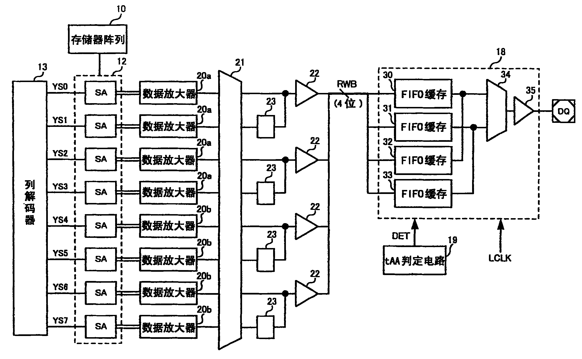
图1为表示本实施方式的DRAM的概要结构的框图。图1所示的DRAM具有:存储数据的存储器阵列10、其周边的行解码器11、读出放大部12、列解码器13、保持地址的行地址缓存14以及列地址缓存15、控制DRAM全体的动作的控制电路16、传送在存储器阵列10与外部之间输入输出的数据的输入缓存电路17以及输出缓存电路18。另外,实际上本实施方式的DRAM还包含有很多其他构成要素,但图1中只示出了与本发明的功能相关联的构成要素。FIG. 1 is a block diagram showing a schematic configuration of a DRAM according to this embodiment. The DRAM shown in FIG. 1 has: a
图1中,存储器阵列10,由形成在矩阵状设置的多根字线与多根位线的交叉部中的多个存储器单元构成。读/写动作时所访问的存储器单元,对应于通过行解码器11所选择的字线与通过列解码器13所选择的位线来设定。行地址缓存14中保持对应行解码器11所选择的字线的行地址,同时,列地址缓存15中保持对应列解码器13所选择的位线的列地址。该行地址缓存14与列地址缓存15各自保持的地址,能够由外部输入的地址信号来设定。In FIG. 1, a
控制电路16对应于被输入的外部命令,向DRAM各部发送给定的控制信号,控制各个的动作。输入给控制电路16的外部命令,根据/RAS信号、/CAS信号、/WE信号、/CS信号的各个组合模式来规定,通过控制电路16的命令解码器(未图示)判断外部命令的种类。另外,控制电路16中被加载了以给定频率互相反转了相位的时钟CLK、/CLK作为外部时钟,被控制为与时钟CLK、/CLK的上升沿或下降沿同步进行动作。另外,控制信号CKE为切换时钟CLK、/CLK的有效、无效的信号。The
如果输入写命令作为外部命令,便将经DQ端子从外部输入的数据依次保持在输入缓存电路17中,以给定的时序写入到存储阵列10中。另外,如果输入了读命令作为外部命令,便由读出放大部12读出保持在存储器阵列10中的数据并放大之后,传送给输出缓存电路18并依次锁存,在给定的时刻经DQ端子传送给外部。另外,虽然图1中未显示,但输入缓存电路17以及输出缓存电路18与存储器阵列10之间,设有传送动作所需要的各种电路以及内部总线。If a write command is input as an external command, the data input from the outside through the DQ terminal is sequentially held in the
接下来,对经由存储器阵列10、输出缓存电路18、DQ端子传送给外部的数据的传送动作与电路结构进行说明。图2为表示对应读对象数据的传送路径的要部结构的框图。本实施方式中,采用在对存储器阵列10的成组读动作时,将对应连续的多个地址数的多个位的数据预取出来并并行传送给输出缓存18,通过这样,能够对应外部的高速传送速度来降低内部的传送速度的构成。Next, the transfer operation and circuit configuration of data transferred to the outside via the
图2中,通过从列解码器13所输出的8个选择信号YS(YS0~YS7),选择读出放大部12中含有的连续的8个读出放大器SA。从存储器阵列10的8个存储器单元所读出的8位的数据,经相补位线对,由8个读出放大器SA同时放大。这样,本实施方式中采用8位预取,将连续的8地址的8位的数据作为对象,进行传送动作。In FIG. 2 , eight consecutive sense amplifiers SA included in
从8个读出放大器SA所输出的8位的数据,被分别与其相连接的8个数据放大器20a、20b放大之后,输入给选择器21。选择器21中,将前半的4个数据放大器20a的输出输出给4个缓存22,同时将后半的4个数据放大器20b的输出输出给延迟部23。通过这样,交互选择经由数据放大器20a的4位的数据,与经由数据放大器20b的4位的数据,从而将每4位数据以不同的时序经缓存22发送给读写总线RWB。也即,读写总线RWB中,将预取的8位分成两份,经读写总线RWB并行传送4位。因此,读写总线RWB的传送动作,由为外部的传送速度的4分之1的内部时钟进行控制。如上所述,DRAM中用来在读写总线RWB中并行传送数据的图2的结构,起到本发明的传送控制机构的作用。另外,读写总线RWB,共用作读出时与写入时的数据的传送路径,但本实施方式中只对读取时的数据的传送动作进行说明。The 8-bit data output from the eight sense amplifiers SA is amplified by the eight
经读写总线RWB并行传送的4位的数据,获取到输出缓存电路18中。如图2所示,输出缓存电路18由4个FIFO缓存30、31、32、33、选择器34、缓存35构成。4个FIFO缓存30~33,是输入经由读写总线RWB并行传送的4位的各个位,保持给定时间之后,按照输入顺序依次取出的电路。如后所述,FIFO缓存30~33,能够选择切换1位锁存电路或6位锁存电路中的任一个。关于各个FIFO缓存30~33的具体构成及动作将在后面说明。输出缓存电路18与确定传送时序的时钟LCLK的上升沿以及下降沿同步,一位位将传送数据传送到外部。另外,时钟LCKL具有与外部时钟CLK相同的频率。The 4-bit data transmitted in parallel via the read/write bus RWB is acquired into the
输出缓存电路18,被tAA判定电路19供给判定信号DET。该tAA判定电路19判定对读取对象数据的访问时间tAA,生成表示访问时间tAA是否超过了给定时间的2值的判定信号DET。访问时间tAA用来规定从指定地址的读命令发出开始,到该地址的开头数据被传送到外部的时间,通常换算成时钟CLK的周期数来表示。输出缓存电路18中,具有上述各个FIFO缓存30~33对应于判定信号DET切换1位锁存电路与6位锁存电路的结构。关于tAA判定电路18的具体构成及动作,将在后面说明。The
接下来,对照图3与图4,对FIFO缓存30的具体电路结构进行说明。如图3所示,FIFO缓存30大体上包括1位锁存电路40、6位锁存电路41、以及选择器42。1位锁存电路40将对经由读写总线RWB的输入数据Din的1次传送动作的1位锁存起来,以给定的时序输出。另外,6位锁存电路41,将对同样的输入数据Din的6次传送动作的总计6位锁存起来,并按照锁存的顺序以给定的时序输出。选择器42对应于tAA判定电路18的判定信号DET,选择切换1位锁存电路40与6位锁存电路41中的任一个路径,输出一体的输出信号Dout。Next, the specific circuit structure of the
1位锁存电路40由两个反相器(inverter)所构成的输入侧开关部101,以及两个反相器的输入输出互相连接的寄存部102构成。开关部101中被加载控制信号CLK0,进行控制,在控制信号CLK0为高电平时,让输入数据Din通过,在控制信号CLK0为低电平时,将输入数据Din截止。该控制信号CLK0,是在发出读写命令后的给定时刻起动,每两个周期输出的脉冲。寄存部102保持通过了开关部101的1位的输入数据Din,之后在开关部101断开的情况下,也能够稳定地继续保存高电平或低电平的保持数据DLa。The 1-
6位锁存电路41通过6级的锁存电路50~55连接而成。图4为表示各级锁存电路50~55的电路结构的图。如图4所示,锁存电路50~55分别由输入侧开关部201、寄存部202、以及输出侧开关部203构成。开关部201、203与上述开关部101具有同样的电路结构,寄存部202具有与上述寄存部102同样的电路结构。输入数据Din经由开关部101与反相器108,输入给各级的输入侧开关部201。另外,各级的输出侧开关部203与选择器42一体连接。The 6-
按照6级的锁存电路50~55的顺序,将选择信号SELa<0>~SELa<5>加载给输入侧的各个开关部201,并且将选择信号SELb<0>~SELb<5>加载给输出侧的各个开关部203。例如,第一级的锁存电路50中的输入输出侧的开关部201、203,在选择信号SELa<0>、SELb<0>为高电平时变为导通状态,另外,在选择信号SELa<0>、SELb<0>为低电平时变为截止状态。第2级以后的锁存电路50~55,也按照同样的控制切换导通状态或截止状态。According to the order of six-
6级的锁存电路50~55的各个寄存部202中,稳定地保持通过了各个开关部201的1位的保持数据DLb<0>~DLb<5>。这种情况下,对应于输入数据Din的取得时序,依次将选择信号SELa<0>~SELa<5>在不同的时刻设为高电平,通过这样能够将6次的传送动作的6位数据锁存在各个锁存电路50~55中。同样,通过依次将选择信号SELb<0>~SELb<5>在不同的时刻设为高电平,能够将上述6位数据以锁存的时序从锁存电路50~55输出。Each
图3中,选择器42由两个开关部103、104构成。一方的开关部103对应于从NAND电路105所输出的控制信号进行切换,让1位锁存电路40的输出信号通过或截止。另一方的开关部104对应于从NAND电路106所输出的控制信号进行切换,让6位锁存电路41的输出信号通过或截止。从选择器42有选择地输出经由开关部103的数据,与经由开关部104的数据,两者作为输出数据Dout发送到外部。In FIG. 3 , the
NAND电路105中,一端被输入判定信号DET,另一端被输入控制信号CLK0R。NAND电路106中,一端经由反相器107被输入判定信号DET的反相信号,另一端被输入控制信号CLK0R。该控制信号CLK0R是与来自输出缓存电路19的传送时序联动的脉冲,此后每2周期进行输出的脉冲。这里,开关部103与开关部104,相对判定信号DET呈反逻辑。也即,在控制信号CLK0R的低电平期间,判定信号DET为低电平时开关部103为截止状态,而开关部104为导通状态,判定信号DET为高电平时,开关部103为导通状态,而开关部104为截止状态。这样,FIFO缓存30中,通过选择器42的控制,在判定信号DET为高电平的情况下,选择1位锁存电路40的路径,在判定信号DET为低电平的情况下,选择6位锁存电路41的路径。In the
接下来,对照图5~图7,对其他三个FIFO缓存31、32、33的具体电路结构进行说明。FIFO缓存31~33的电路结构,与图3的FIFO缓存30大体上相同。因此,给图5~图7的各个电路结构中,与图3的FIFO缓存相同的构成要素标注相同的符号,省略其说明。另外,如图5~图7所示,选择器42的输出侧,FIFO缓存31中设有输出侧电路61,FIFO缓存32中设有输出侧电路62,FIFO缓存33中设有输出侧电路63。Next, specific circuit configurations of the other three
各个FIFO缓存31~33的输出侧电路61~63,均由寄存部301、开关部302、以及反相器303构成。并且,经反相器303给开关部302分别加载不同的控制信号。也即,图5的输出侧电路61中加载控制信号CLK1F,图6的输出侧电路62中加载控制信号CLK2R,图7的输出侧电路63中加载控制信号CLK3F。The
各个输出侧电路61~63中,从选择器42所输出的信号被输入给寄存部301,稳定地保持低电平或高电平的1位数据。并且,开关部302在对应的控制信号CLK1F、CLK2R、CLK3F为高电平时变为导通状态,低电平时变为截止状态。因此,通过适当控制各个控制信号CLK1F、CLK2R、CLK3F变为高电平的时序,就能够将来自4个FIFO缓存30~33的输出信号Dout调整为分别稍有不同的时序。In each of the output-
例如,能够让FIFO缓存30、32与时钟LCLK的上升沿同步,FIFO缓存31、33与时钟LCLK的下降沿同步。这种情况下,在相当于时钟CLK的2周期的期间内,能够让4个FIFO缓存30~33的各个输出Dout循环一周。另外,关于各个FIFO缓存30~33的动作时的动作波形,将在后面说明。For example, the FIFO buffers 30 and 32 can be synchronized with the rising edge of the clock LCLK, and the FIFO buffers 31 and 33 can be synchronized with the falling edge of the clock LCLK. In this case, each output Dout of the four
接下来回到图2,FIFO缓存30~33的各个输出信号Dout,输入给选择器34。选择器34中,根据与时钟CLK的同步关系,切换控制一体化的FIFO缓存30、32的输出信号Dout,与一体化的FIFO缓存31、33的输出信号Dout。另外,从选择器34所输出的信号,经缓存35串行传送,从DQ端子传送到外部。Next, returning to FIG. 2 , each output signal Dout of the FIFO buffers 30 - 33 is input to the
另外,图2的要部构成中,只示出了1系统的传送路径以及1个输出缓存电路18,但需要对应于DRAM的位结构的多个传送路径与多个输出缓存电路18。例如,如果以I/O数为16位的结构为前提,则图2的要部构成中,需要设置16系统的传送路径与16个输出缓存电路18。如果着眼于6位锁存电路41,则由于1个输出缓存电路18中保持有6×4=24位的数据,因此16位(I/O数)构成中全部保持有24×16=384位数据。另外,并不仅限于16位(I/O数)构成,还可以对I/O数为P位的构成的DRAM,设置P个输出缓存18,使用本发明。2 shows only one system of transmission paths and one
本实施方式中,如前所述,输出缓存电路18的动作模式,具有将传送数据的路径切换到1位锁存电路40侧的动作模式,与切换到6位锁存电路41侧的动作模式。动作模式的切换,在tAA判定电路19中对应于访问时间tAA与给定的设定值的大小关系来控制,在访问时间tAA没达到给定的设定时间时,设定1位锁存电路40的路径,在访问时间tAA超过了给定的设定时间时,设定6位锁存电路41的路径。In this embodiment, as described above, the operation mode of the
例如,在给时钟CLK的周期乘以CAS等待时间,规定访问时间tAA的情况下,对于高速的时钟CLK,访问时间tAA变短,对于低速的时钟CLK,访问时间tAA变长。以下,对使用高速的时钟CLK设定1位锁存电路40的路径情况,与使用低速的时钟CLK设定6位锁存电路41的路径的情况的动作的不同进行说明。For example, when the cycle of the clock CLK is multiplied by the CAS latency to define the access time tAA, the access time tAA is shortened for a high-speed clock CLK and lengthened for a low-speed clock CLK. The difference in operation between the case where the high-speed clock CLK is used to set the path of the 1-
图8中,示出了使用周期1.25ns的高速的时钟CLK,在输出缓存电路18中设定1位锁存电路40的路径的情况下的动作波形图。给时钟CLK的各个周期标注编号0~15,表示周期数的推移。以在周期0发出读命令RD作为外部命令,此后每4周期依次发出读命令的成组读动作为前提。如图8所示,对应于各个读命令RD,其两个周期后输出对应于解码结果的命令信号MR的脉冲。进而,从命令信号MR开始经过了给定时间后,选择指定地址的位线的选择信号YS上升。通过这样,选择作为读出对象的连续的8地址的位线,对应的存储单元的数据被8个读出放大器SA放大。FIG. 8 shows an operation waveform diagram in the case where the path of the 1-
接下来,8位的数据发送给数据放大器20a、20b,其输出信号DA在周期7输出。之后,经过选择器21、缓存22、延迟部23被分为4位,前4位数据在周期8被传送给读写总线RWB。另外,后4位数据在周期10被传送给读写总线RWB。Next, the 8-bit data is sent to the
另外,图8中将各4位的数据表示为0123、4567。此后也对应于后继的读命令RD,将每4位的数据表示为89AB、CDEF。In addition, in FIG. 8, each 4-bit data is shown as 0123, 4567. Thereafter, each 4-bit data is represented as 89AB, CDEF corresponding to the subsequent read command RD.
传送开头的数据0123的时序之后,控制信号CLK0的脉冲上升。通过这样,数据0123的各个位分配给FIFO缓存30~33,分别通过1位锁存电路40的开关部101。这里,控制信号CLK0的脉冲时序,依赖于DRAM核心的动作速度设定。另外,由于判定信号DET为高电平,因此1位锁存电路40中将各个1位数据作为保持数据DLa(数据0123的各位)锁存起来。此时,图8中示出了在时序T0中开头的数据0123被锁存的状态。After the timing at which the
这里,对4个FIFO缓存30~33所加载的4个控制信号CLK0R、CLK1F、CLK2R、CLK3F,其时序依次每次错开时钟CLK的半周期。也即,时序T1中最初的时钟CLK0R的脉冲上升之后,半周期后时钟CLK1F的脉冲上升,1周期后时钟CLK2R的脉冲上升,1.5周期后时钟CLK3F的脉冲上升。这样,4位数据0123的各个位,按照FIFO缓存30、31、32、33的顺序,以上述时序输出。Here, the timings of the four control signals CLK0R, CLK1F, CLK2R, and CLK3F loaded by the four FIFO buffers 30-33 are sequentially staggered by half periods of the clock CLK each time. That is, after the pulse of the first clock CLK0R rises in sequence T1, the pulse of the clock CLK1F rises half a cycle later, the pulse of the clock CLK2R rises one cycle later, and the pulse of the clock CLK3F rises 1.5 cycles later. In this way, each bit of the 4-
对后继的4位数据4567也通过同样的时序进行控制,因此传送对象的8位数据01234567,与时钟CLK的上升/下降沿同步,从DQ端子串行传送。进而对后继的读命令RD也重复同样的控制,通过这样,能够在成组读完成之前,重复给定位数的数据,从DQ端子串行传送。The subsequent 4-
图8中可以得知,从周期0中发出最初的读命令RD之后,到在周期10中从DQ端子输出开头的位0之间,需要10周期的访问时间tAA。这种情况下,计算出tAA=10×1.25ns=12.5ns。这样,在访问时间tAA到来的时序中,只将数据0123传送给输出缓存18,后继的数据4567的传送没有开始。也即,由于对访问时间tAA,将到控制信号CLK0的第2次上升沿的时间设定地较晚,因此确保了从控制信号CLK0R的下降沿到控制信号CLK0的上升沿之间的时间tm。这里,时间tm是1位锁存电路40的动作余裕(margin)。这样的情况下,由于各个FIFO缓存30~33中保持1位就可以,因此设定1位锁存电路40的路径。It can be seen from FIG. 8 that an access time tAA of 10 cycles is required between the first read command RD in
接下来,图9中示出了将上述的时钟CLK低速化,使用2倍的周期2.5ns的时钟CLK,在输出缓存电路18中设定6位锁存电路41的路径的情况下的动作波形图。图9中,由于通过与图8相同的宽度表示时钟CLK的各个周期,因此实际的时间轴为图8的两倍。这种情况下,基于最初的读命令RD,与此后的每4周期依次发出读命令RD的成组读的动作,也与图8一样。Next, FIG. 9 shows the operation waveform in the case where the above-mentioned clock CLK is slowed down, and the clock CLK with twice the period of 2.5 ns is used to set the path of the 6-
如图9所示,输出列解码器13的选择信号YS、数据放大器20a、20b的输出信号DA的时序,以及读写总线RWB中的最初的4位的传送时序,需要与图8相同程度的时间,但周期数减半。从图9可以得知,第2个读命令RD的发出时刻,经过了读写总线RWB的最初的数据0123向输出缓存电路18的传送动作尚未完成。另外,计算出访问时间tAA为tAA=10×2.5ns=25ns,但与图8不同,在访问时间tAA的到达时刻之前,至少先行了控制信号CLK0的4次上升沿。这种情况下,如果各个FIFO缓存30~33中保持1位数据,就会来不及,因此设定6位锁存电路41的路径。As shown in FIG. 9, the timing of outputting the selection signal YS of the
图9中,控制信号CLK0R,与4位数据的传送时序同步上升,各个位分配给FIFO缓存30~33。各个FIFO缓存30~33的6位锁存电路41中,控制为让6级锁存电路50~55依次变为导通状态。因此,输入侧的选择信号SELa<0:5>每2周期进行切换,依次变为高电平。In FIG. 9, the control signal CLK0R rises synchronously with the transmission timing of 4-bit data, and each bit is allocated to FIFO buffers 30-33. In the 6-
4个FIFO缓存30~33中,将开头的数据0123的各个位作为第一级的各个锁存电路50的保持数据DLb<0>锁存起来之后,过两个周期,将第2个数据4567的各个位作为第2级的各个锁存电路51的保持数据DLb<1>锁存起来,之后也一样,每隔两个周期将各个数据依次锁存到锁存电路50~55中。In the four FIFO buffers 30-33, after each bit of the
周期9之后,输出控制信号CLK0R与输出侧的选择信号SELb<0:5>。这种情况下也一样,每两周期切换选择信号SELb<0:5>,4个FIFO缓存30~33中,按照锁存顺序输出各个锁存电路50~55的保持数据DLb<0>~DLb<5>。各个4位数据经FIFO缓存器30~33的选择器42,作为输出数据Dout输出。对各个读命令RD也重复同样的控制,通过这样,传送对象数据与时钟CLK的上升/下降沿同步,从DQ端子串行传送到外部。After
接下来,对tAA判定电路19的构成与动作,以及作为判定信号DET的比较基准的设定值的条件进行说明。图10中示出了tAA判定电路19的具体电路结构。图10所示的tAA电路19,包含有RS锁存器401、402、开关部403、404、NOR电路405、406、NAND电路407、408、反相器409、410、411、以及延迟部412。Next, the configuration and operation of the
两个RS锁存器401、402,对应于被输入后述的MRST信号以及RESET信号的OR电路406的输出被复位。因此,如果MRST信号或RESET信号变为高电平,RS锁存器401、402就被复位。RS锁存器401,对应于被输入控制信号CLKR以及经延迟部412与反相器401输入该控制信号CLKR的OR电路405的输出而被复位。因此,从OR电路405输出在控制信号CLKR的脉冲的下降沿变为低电平的脉冲,通过这样来复位RS锁存器401。The two RS latches 401 and 402 are reset according to the output of the
另外,能够对应于延迟部412的延迟时间,调整RS锁存器401的设置电平的宽度。RS锁存器402,对应于经反相器410所输入的控制信号CLK0被设置。因此,在输出控制信号CLK0的脉冲时,RS锁存器402被设置。In addition, the width of the setting level of the
3个反相器所构成的前级的开关部403,在RS锁存器401所输出的锁存信号CLKRd为低电平时,让RS锁存器402所输出的锁存信号CLK0D通过。另外,在锁存信号CLKRd为高电平时,开关部403中将锁存信号CLK0d截止,通过NOR电路407的输入输出的连接,稳定地保持之前的通过时的状态。The
另外,3个反相器所构成的后级的开关部404,在RS锁存器401所输出的锁存信号CLKRd为高电平时,让上述NOR电路407的输出通过。另外,在锁存信号CLKRd为低电平时,开关部404中将NOR电路407的输出截止,通过后级的NOR电路408的输入输出的连接,稳定地保持之前的通过时的状态。NOR电路408的输出,通过反相器411作为判定信号DET输出。In addition, the
以下,对使用高速的时钟CLK设定1位锁存电路40的路径的情况,与使用低速的时钟CLK设定6位锁存电路41的路径的情况下,各个tAA判定电路19的动作的不同进行说明。Hereinafter, the operation of each
首先,图11中与图8一样,示出了使用周期1.25ns的高速的时钟CLK的情况下的tAA判定电路19的动作波形图。本实施方式中,在作为对DRAM的初始设定中所使用的模式寄存器(未图示)的设定命令的MRS命令的发出时,执行基于tAA判定电路19的动作。图11中,在周期0发出设定命令MRS,两周期后,对应于解码结果输出MRST信号的脉冲。接下来,在周期4中发出读命令RD,之后的成组读动作,与图8一样进行。First, FIG. 11 shows an operation waveform diagram of the
一旦因设定命令MRS的发出使得MRST信号变为高电平,便如上所述,复位图10的RS锁存器401、402,并且一端被加载了MRST信号的两个NAND电路407、408的输出变为高电平。之后,在控制信号CLKR保持低电平的期间,判定信号DET继续保持低电平。另外,该期间中,前级的开关部403变为导通状态,后级的开关部404变为截止状态,NAND电路407的输出变为低电平。Once the MRST signal becomes high due to the sending of the setting command MRS, as described above, the RS latches 401, 402 in FIG. 10 are reset, and one end of the two
这里,让控制信号CLKR比加载给输出缓存电路19的控制信号CLK0R早两个周期上升。因此如图11所示,先行于控制信号CLK0R的脉冲,在周期11的期间中输出控制信号CLKR的脉冲。图10中,一旦在控制信号CLKR的下降沿,锁存信号CLKRd变为高电平,便将前级的开关部403切换为截止状态,将后级的开关部404切换为导通状态。于是两个NAND电路407、408相连接,后级的NAND电路408的输出从高电平变为低电平,因此时序T2中,判定信号DET从低电平变为高电平。Here, the control signal CLKR is made to rise two cycles earlier than the control signal CLK0R applied to the
另外,控制信号CLK0是与读写总线RWB的传送时序同步的脉冲,图11的情况下,最初的上升是判定信号DET已经为高电平的时序T3,因此,由开关部402截止了控制信号CLK0的变化。这样,在之后RS锁存器401被复位之前,判定信号DET继续保持高电平。所以,输出缓存电路18中,设定1位锁存电路40的路径。这样,通过判断控制信号CLKR先行于控制信号CLK0,能够对应于图11的访问时间tAA的12.5ns,执行基于1位锁存电路40的路径的适当传送动作。In addition, the control signal CLK0 is a pulse synchronized with the transfer timing of the read/write bus RWB. In the case of FIG. CLK0 changes. In this way, until the
接下来,图12中与图9一样,示出了使用周期2.5ns的低速的时钟CLK的情况下的tAA判定电路19的动作波形图。图12中,通过对应设定命令MRS的MRST信号,复位RS锁存器401、402这一点,与图11一样。但是,图12中控制信号CLKR的脉冲与控制信号CLK0的脉冲的时序,与图11不同。也即,关于控制信号CLKR与图11一样,先行于控制信号CLK0R两个周期,在周期11的期间中上升,与此相对,由读写总线RWB的传送时序所规定的控制信号CLK0,即使设想为与图11相同的时间,也由于时间轴变为两倍,周期数减半,从而提前。Next, FIG. 12 shows an operation waveform diagram of the
因此,与图11的情况相反,在先行于控制信号CLKR的时刻T4输出控制信号CLK0的脉冲。通过这样,图10的RS锁存器402被设置,锁存信号CLKRd变为高电平,经由处于导通状态的前级的开关部403,NOR电路407的输出从低电平变为高电平。之后,在控制信号CLKR的下降沿,锁存信号CLKRd变为高电平,将前级的开关部403切换为截止状态,将后级的开关部404切换为导通状态。通过这样,两个NAND电路407、408相连接,后级的NAND电路380的输出变为高电平,因此判定信号DET继续保持低电平的状态。Therefore, contrary to the case of FIG. 11 , the pulse of the control signal CLK0 is output at time T4 preceding the control signal CLKR. In this way, the
这样,在控制信号CLK0的脉冲先行,之后控制信号CLKR的脉冲进行变化的情况下,如图11所示,判定信号DET保持高电平不变。因此输出缓存电路18中,设定6位锁存电路41的路径。也即,通过判定控制信号CLK0先行于控制信号CLKR,能够对应于图12的访问时间tAA的25ns,执行基于6位锁存电路41的路径的适当传送动作。In this way, when the pulse of the control signal CLK0 precedes and the pulse of the control signal CLKR changes thereafter, as shown in FIG. 11 , the determination signal DET remains at a high level. Therefore, in the
接下来,对根据tAA判定电路19的切换条件进行说明。图11与图12中,将最初的读命令RD的发出时刻作为起点,到控制信号CLK0的上升沿的时间表示为t1,到控制信号CLKR的下降沿的时间表示为t2。这种情况下,tAA判定电路19中,判定时间t1与时间t2的大小关系。一般来说,时间t1通过DRAM核心的访问动作的实际值设定,例如假设为:Next, the switching conditions of the
t1=10.9ns (1)t1=10.9ns (1)
另外,时间t2使用时钟CLK的周期tCK、CAS等待时间CL、以及输出缓存电路18中的延迟时间td0,满足以下关系:In addition, the time t2 uses the cycle tCK of the clock CLK, the CAS waiting time CL, and the delay time td0 in the
t2=(CL-2)×tCK-td0 (2)t2=(CL-2)×tCK-td0 (2)
另外,延迟时间td0为0.5ns程度。这种情况下,切换1位锁存电路40与6位锁存电路41的各个路径的条件为:In addition, the delay time td0 is about 0.5 ns. In this case, the conditions for switching the respective paths of the 1-
(a)t1≥t2的情况下,设定1位锁存电路40的路径(a) In the case of t1≥t2, the path of the 1-
(b)t1<t2的情况下,设定6位锁存电路41的路径(b) In the case of t1<t2, the path of the 6-
因此,如果将式(1)、(2)代入到条件(a)中,便导出:Therefore, if formulas (1) and (2) are substituted into condition (a), it is derived:
tCL≤11.4/(CL-2) (3)tCL≤11.4/(CL-2) (3)
另外,如果将式(1)、(2)代入到条件(b)中,便导出:In addition, if formulas (1) and (2) are substituted into condition (b), it is derived:
tCL>11.4/(CL-2) (4)tCL>11.4/(CL-2) (4)
例如,在CL=10的情况下,条件(a)变为tCK≤1.43ns,条件(b)变为tCL>1.43ns。For example, in the case of CL=10, the condition (a) becomes tCK≦1.43ns, and the condition (b) becomes tCL>1.43ns.
如上所述,根据本实施方式,能够对应于tAA检测电路19的判定信号DET,对各个FIFO缓存30~33,并列设置1位锁存电路40与6位锁存电路41并分别使用。对时钟CLK的频率变动,虽然与周期数连动的访问时间tAA进行伸缩,但DRAM核心的动作速度不会发生很大变化。因此在使用高速的时钟CLK的情况下,访问时间tAA缩短,不需要锁存多个位。与此相对,在使用低速的时钟CLK的情况下,访问时间tAA延长,需要锁存更多个位。本实施方式的构成中,对高速的时钟CLK使用1位锁存电路40,锁存最小限度的数据,对低速的时钟CLK使用6位锁存电路41,锁存足够的数据,因此能够可靠地对应动作条件的变动。所以,在使用高速的时钟CLK的情况下,能够构成最短的路径,实现进一步的高速化,并且还能够缩小传送时进行动作的电路规模,降低访问时的动作电流。另外,在使用低速的时钟CLK的情况下,即使因动作条件的变动等导致应当保持的数据增大,也能够由锁存电路可靠地锁存,从而能够防范误动作于未然。As described above, according to the present embodiment, the 1-
以上,根据本实施方式对本发明的内容进行了具体说明,但本发明并不仅限于上述实施方式,还可以在不脱离其要点的范围内进行各种变更。例如,本实施方式的输出缓存电路18,采用并列设有能够切换1位锁存电路40与6位锁存电路41的结构,但还可以采用并列设有能够切换的更大范围的M位锁存电路与N(N>M)位锁存电路的结构。这种情况下,最好考虑半导体存储装置中的多种动作条件,选择最佳的M、N。例如,将1位锁存电路40置换成2位锁存电路,并与6位锁存电路41并列设置的情况下,上述(1)~(4)式能够表示为下面的(1)’~(4)’式。As mentioned above, although the content of this invention was concretely demonstrated based on this embodiment, this invention is not limited to the said embodiment, Various changes are possible in the range which does not deviate from the summary. For example, the
t1=10.9ns+2×tCK (1)’t1=10.9ns+2×tCK (1)’
t2=(CL-2)×tCK-td0 (2)’t2=(CL-2)×tCK-td0 (2)’
tCL≤11.4/(CL-4) (3)’tCL≤11.4/(CL-4) (3)’
tCL>11.4/(CL-4) (4)’tCL>11.4/(CL-4) (4)’
另外,本实施方式中,对预取的位数为8,经由读写总线RWB并行传送的位数为4的情况进行了说明,但该位数也能够作为设计事项来适当变更。进而,输出缓存电路18或tAA检测电路19的具体电路结构,能够通过多种多样的构成来实现,只要能够实现同等的功能就可以。In addition, in this embodiment, a case has been described in which the number of bits to be prefetched is 8 and the number of bits to be transferred in parallel via the read/write bus RWB is 4, but the number of bits can be appropriately changed as a design matter. Furthermore, the specific circuit configuration of the
本发明并不限于上述的实施方式,只要不脱离本发明的范围各种变更和修改都可以。The present invention is not limited to the above-described embodiments, and various changes and modifications are possible without departing from the scope of the present invention.
本申请基于日本2005年9月16日的申请号为2005-271197的发明申请,在此其所有内容明确地通过引用而被并入。This application is based on Invention Application No. 2005-271197 filed on September 16, 2005 in Japan, the entire contents of which are hereby expressly incorporated by reference.
Claims (12)
Applications Claiming Priority (2)
| Application Number | Priority Date | Filing Date | Title |
|---|---|---|---|
| JP2005271197 | 2005-09-16 | ||
| JP2005271197A JP4600825B2 (en) | 2005-09-16 | 2005-09-16 | Semiconductor memory device |
Publications (2)
| Publication Number | Publication Date |
|---|---|
| CN1933016A CN1933016A (en) | 2007-03-21 |
| CN100541648C true CN100541648C (en) | 2009-09-16 |
Family
ID=37878792
Family Applications (1)
| Application Number | Title | Priority Date | Filing Date |
|---|---|---|---|
| CNB200610154020XA Active CN100541648C (en) | 2005-09-16 | 2006-09-15 | semiconductor storage device |
Country Status (3)
| Country | Link |
|---|---|
| US (1) | US7426144B2 (en) |
| JP (1) | JP4600825B2 (en) |
| CN (1) | CN100541648C (en) |
Families Citing this family (19)
| Publication number | Priority date | Publication date | Assignee | Title |
|---|---|---|---|---|
| JP4470183B2 (en) | 2006-08-28 | 2010-06-02 | エルピーダメモリ株式会社 | Semiconductor memory device |
| JP5666077B2 (en) * | 2007-07-04 | 2015-02-12 | ピーエスフォー ルクスコ エスエイアールエルPS4 Luxco S.a.r.l. | Address counter, semiconductor memory device having the same, and data processing system |
| JP5458235B2 (en) | 2007-07-10 | 2014-04-02 | ピーエスフォー ルクスコ エスエイアールエル | Semiconductor memory device and LIO dividing method |
| US8364901B2 (en) * | 2009-02-13 | 2013-01-29 | Micron Technology, Inc. | Memory prefetch systems and methods |
| AU2010325518A1 (en) | 2009-11-30 | 2012-06-14 | F.Hoffmann-La Roche Ag | Analyte monitoring and fluid dispensing system |
| US8711639B2 (en) | 2010-11-02 | 2014-04-29 | Micron Technology, Inc. | Data paths using a first signal to capture data and a second signal to output data and methods for providing data |
| JP5632269B2 (en) * | 2010-11-26 | 2014-11-26 | ピーエスフォー ルクスコ エスエイアールエルPS4 Luxco S.a.r.l. | Semiconductor device |
| US9411722B2 (en) * | 2013-03-04 | 2016-08-09 | Sandisk Technologies Llc | Asynchronous FIFO buffer for memory access |
| CN111309284B (en) | 2015-05-28 | 2024-02-02 | 铠侠股份有限公司 | Semiconductor device |
| US10019170B2 (en) * | 2016-03-30 | 2018-07-10 | Micron Technology, Inc. | Controlling timing and edge transition of a delayed clock signal and data latching methods using such a delayed clock signal |
| JP2017219586A (en) * | 2016-06-03 | 2017-12-14 | 株式会社ジャパンディスプレイ | Signal supply circuit and display device |
| CN106328183B (en) * | 2016-09-23 | 2018-08-31 | 山东师范大学 | A kind of improved storage system and method |
| US10490238B2 (en) * | 2017-06-29 | 2019-11-26 | SK Hynix Inc. | Serializer and memory device including the same |
| US10607692B2 (en) * | 2017-06-29 | 2020-03-31 | SK Hynix Inc. | Serializer and memory device including the same |
| KR102517463B1 (en) * | 2018-04-27 | 2023-04-04 | 에스케이하이닉스 주식회사 | Semiconductor device |
| KR102752629B1 (en) * | 2019-12-04 | 2025-01-10 | 에스케이하이닉스 주식회사 | Memory device and operating method thereof |
| US11567868B2 (en) * | 2020-11-13 | 2023-01-31 | Taiwan Semiconductor Manufacturing Company, Ltd. | Method for copying data within memory device, memory device, and electronic device thereof |
| CN120766738A (en) * | 2020-12-28 | 2025-10-10 | 铠侠股份有限公司 | Memory system and semiconductor storage device |
| CN112687305B (en) * | 2021-01-05 | 2024-05-10 | 深圳芯邦科技股份有限公司 | Data storage circuit |
Family Cites Families (7)
| Publication number | Priority date | Publication date | Assignee | Title |
|---|---|---|---|---|
| JP2817679B2 (en) * | 1995-09-20 | 1998-10-30 | 日本電気株式会社 | Semiconductor memory |
| JPH11176158A (en) * | 1997-12-10 | 1999-07-02 | Fujitsu Ltd | Latch circuit, data output circuit, and semiconductor device having the same |
| JP2001243770A (en) * | 2000-02-25 | 2001-09-07 | Fujitsu Ltd | Synchronous semiconductor memory device and data reading method thereof |
| KR100438778B1 (en) * | 2001-11-07 | 2004-07-05 | 삼성전자주식회사 | Synchronous semiconductor memory device having wave pipeline structure and wave pipeline control method thereof |
| JP4607444B2 (en) * | 2002-11-18 | 2011-01-05 | 三星電子株式会社 | Semiconductor device, data retrieval circuit, memory cell array interpretation method, and data retrieval method |
| KR100518564B1 (en) * | 2003-04-03 | 2005-10-04 | 삼성전자주식회사 | Ouput multiplexing circuit and method for double data rate synchronous memory device |
| KR100604948B1 (en) * | 2005-08-17 | 2006-07-31 | 삼성전자주식회사 | Wave pipeline output circuit of synchronous memory device |
-
2005
- 2005-09-16 JP JP2005271197A patent/JP4600825B2/en not_active Expired - Lifetime
-
2006
- 2006-09-15 CN CNB200610154020XA patent/CN100541648C/en active Active
- 2006-09-15 US US11/521,489 patent/US7426144B2/en active Active
Also Published As
| Publication number | Publication date |
|---|---|
| JP4600825B2 (en) | 2010-12-22 |
| US20070076474A1 (en) | 2007-04-05 |
| JP2007087436A (en) | 2007-04-05 |
| US7426144B2 (en) | 2008-09-16 |
| CN1933016A (en) | 2007-03-21 |
Similar Documents
| Publication | Publication Date | Title |
|---|---|---|
| CN100541648C (en) | semiconductor storage device | |
| US6262938B1 (en) | Synchronous DRAM having posted CAS latency and method for controlling CAS latency | |
| JP2817679B2 (en) | Semiconductor memory | |
| KR100306966B1 (en) | Synchronous Burst Semiconductor Memory Device | |
| US7801696B2 (en) | Semiconductor memory device with ability to adjust impedance of data output driver | |
| US7327613B2 (en) | Input circuit for a memory device | |
| US6337809B1 (en) | Semiconductor memory device capable of improving data processing speed and efficiency of a data input and output pin and related method for controlling read and write | |
| US7715245B2 (en) | Pipe latch device of semiconductor memory device | |
| US6061292A (en) | Method and circuit for triggering column select line for write operations | |
| CN1790544B (en) | Semiconductor memory device | |
| KR100362193B1 (en) | Data Output Device of DDR SDRAM | |
| KR20020004859A (en) | Semiconductoro memorty device | |
| US7085192B2 (en) | Semiconductor integrated circuit device | |
| KR100719377B1 (en) | Semiconductor memory device that reads data patterns | |
| US6292430B1 (en) | Synchronous semiconductor memory device | |
| US7212449B2 (en) | Data output device of semiconductor memory device | |
| US6973006B2 (en) | Predecode column architecture and method | |
| US7057966B2 (en) | Semiconductor memory device for reducing current consumption in operation | |
| US6714471B2 (en) | Semiconductor memory device having preamplifier with improved data propagation speed | |
| JP4127054B2 (en) | Semiconductor memory device | |
| US6504767B1 (en) | Double data rate memory device having output data path with different number of latches | |
| US8107315B2 (en) | Double data rate memory device having data selection circuit and data paths |
Legal Events
| Date | Code | Title | Description |
|---|---|---|---|
| C06 | Publication | ||
| PB01 | Publication | ||
| C10 | Entry into substantive examination | ||
| SE01 | Entry into force of request for substantive examination | ||
| C14 | Grant of patent or utility model | ||
| GR01 | Patent grant | ||
| ASS | Succession or assignment of patent right |
Owner name: MICRON TECHNOLOGY, INC. Free format text: FORMER OWNER: ELPIDA MEMORY INC. Effective date: 20140512 |
|
| C41 | Transfer of patent application or patent right or utility model | ||
| TR01 | Transfer of patent right |
Effective date of registration: 20140512 Address after: Idaho Patentee after: Micron Technology, Inc. Address before: Tokyo, Japan Patentee before: Elpida Memory Inc. |