CN100536153C - Pixel sensor structure and manufacturing method of semiconductor structure - Google Patents
Pixel sensor structure and manufacturing method of semiconductor structure Download PDFInfo
- Publication number
- CN100536153C CN100536153C CNB2006101641183A CN200610164118A CN100536153C CN 100536153 C CN100536153 C CN 100536153C CN B2006101641183 A CNB2006101641183 A CN B2006101641183A CN 200610164118 A CN200610164118 A CN 200610164118A CN 100536153 C CN100536153 C CN 100536153C
- Authority
- CN
- China
- Prior art keywords
- funnel
- shaped
- light pipe
- cavity
- layer
- Prior art date
- Legal status (The legal status is an assumption and is not a legal conclusion. Google has not performed a legal analysis and makes no representation as to the accuracy of the status listed.)
- Active
Links
Images


Classifications
-
- G—PHYSICS
- G01—MEASURING; TESTING
- G01J—MEASUREMENT OF INTENSITY, VELOCITY, SPECTRAL CONTENT, POLARISATION, PHASE OR PULSE CHARACTERISTICS OF INFRARED, VISIBLE OR ULTRAVIOLET LIGHT; COLORIMETRY; RADIATION PYROMETRY
- G01J1/00—Photometry, e.g. photographic exposure meter
- G01J1/02—Details
- G01J1/04—Optical or mechanical part supplementary adjustable parts
- G01J1/0407—Optical elements not provided otherwise, e.g. manifolds, windows, holograms, gratings
- G01J1/0422—Optical elements not provided otherwise, e.g. manifolds, windows, holograms, gratings using light concentrators, collectors or condensers
-
- G—PHYSICS
- G01—MEASURING; TESTING
- G01J—MEASUREMENT OF INTENSITY, VELOCITY, SPECTRAL CONTENT, POLARISATION, PHASE OR PULSE CHARACTERISTICS OF INFRARED, VISIBLE OR ULTRAVIOLET LIGHT; COLORIMETRY; RADIATION PYROMETRY
- G01J1/00—Photometry, e.g. photographic exposure meter
- G01J1/02—Details
- G01J1/04—Optical or mechanical part supplementary adjustable parts
- G01J1/0488—Optical or mechanical part supplementary adjustable parts with spectral filtering
Landscapes
- Physics & Mathematics (AREA)
- General Physics & Mathematics (AREA)
- Spectroscopy & Molecular Physics (AREA)
- Solid State Image Pick-Up Elements (AREA)
Abstract
一种像素传感结构及其形成方法。所述结构包括(a)半导体衬底和(b)在所述半导体衬底上的光收集区域。所述结构还包括在所述光收集区域的顶部上的漏斗状光导管。所述漏斗状光导管包括(i)在所述光收集区域的的顶部上的底部柱状部分,以及(ii)具有锥形形状且在所述底部柱状部分的顶部上并与所述底部柱状部分直接物理接触的漏斗状部分,其中所述漏斗状部分的截面具有凸面形状。所述结构还包括在所述漏斗状光导管的顶部上的滤色区域。
A pixel sensing structure and a forming method thereof. The structure includes (a) a semiconductor substrate and (b) a light collection region on the semiconductor substrate. The structure also includes a funnel-shaped light pipe on top of the light collection area. The funnel-shaped light pipe includes (i) a bottom cylindrical portion on top of the light collection area, and (ii) has a tapered shape on top of and connected to the bottom cylindrical portion. A funnel-shaped portion in direct physical contact, wherein the cross-section of said funnel-shaped portion has a convex shape. The structure also includes a color filter region on top of the funnel-shaped light pipe.
Description
技术领域 technical field
本发明涉及像素传感器,更具体涉及具有漏斗状光导管的像素传感器。The present invention relates to pixel sensors, and more particularly to pixel sensors having funnel-shaped light pipes.
背景技术 Background technique
一些先进的像素传感器实现了具有微透镜的垂直光导管,其中微透镜用于将光聚焦到光导管中。然而,需要一种不具有现有技术的微透镜的像素传感器结构。Some advanced pixel sensors implement vertical light pipes with microlenses used to focus light into the light pipe. However, there is a need for a pixel sensor structure that does not have prior art microlenses.
发明内容 Contents of the invention
本发明提供一种像素传感器结构,其包括:(a)半导体衬底;(b)在所述半导体衬底上的光收集区域;以及(c)在所述光收集区域的顶部上的漏斗状光导管,其中所述漏斗状光导管包括(i)在所述光收集区域的顶部上的底部柱状部分,以及(ii)具有锥形形状且在所述底部柱状部分的顶部上并与所述底部柱状部分直接物理接触的漏斗状部分。The present invention provides a pixel sensor structure comprising: (a) a semiconductor substrate; (b) a light collection region on the semiconductor substrate; and (c) a funnel-shaped A light pipe, wherein the funnel-shaped light pipe includes (i) a bottom cylindrical portion on top of the light collection area, and (ii) has a tapered shape on top of the bottom cylindrical portion and is connected to the The funnel-shaped part with which the bottom columnar part is in direct physical contact.
本发明还提供一种半导体结构的制造方法,其包括以下步骤:提供一种结构,其包括(i)半导体衬底,(ii)在所述半导体衬底上的光收集区域,以及(iii)在所述光收集区域和所述半导体衬底上的BEOL(后段制程)层;蚀刻所述BEOL层,以便在所述BEOL层中形成漏斗状空腔,其中所述漏斗状空腔的截面具有锥形形状;在所述蚀刻所述BEOL层以便在所述BEOL层中形成所述漏斗状空腔之后,通过所述漏斗状空腔进一步蚀刻所述BEOL层,以便在所述BEOL层中形成柱状空腔,其中所述柱状空腔在所述光收集区域正上方且在所述漏斗状空腔正下方;以及在所述柱状空腔和所述漏斗状空腔中形成漏斗状光导管。The present invention also provides a method of fabricating a semiconductor structure, comprising the steps of: providing a structure comprising (i) a semiconductor substrate, (ii) a light collection region on the semiconductor substrate, and (iii) A BEOL (Back End of Line) layer on the light collection region and the semiconductor substrate; etching the BEOL layer to form a funnel-shaped cavity in the BEOL layer, wherein a section of the funnel-shaped cavity having a tapered shape; after said etching said BEOL layer to form said funnel-shaped cavity in said BEOL layer, said BEOL layer is further etched through said funnel-shaped cavity so that in said BEOL layer forming a columnar cavity, wherein the columnar cavity is directly above the light collection region and directly below the funnel-shaped cavity; and forming a funnel-shaped light pipe in the columnar cavity and the funnel-shaped cavity .
本发明还提供一种光传感结构,其包括:(a)半导体衬底;(b)在所述半导体衬底上的光收集区域;(c)在所述半导体衬底和所述光收集区域上的BEOL(后段制程)层;以及(d)在所述光收集区域的顶部上且在所述BEOL层中的漏斗状光导管,其中所述漏斗状光导管包括(i)在所述光收集区域的顶部上的底部柱状部分,(ii)具有锥形形状且在所述底部柱状部分的顶部上并与所述底部柱状部分直接物理接触的漏斗状部分,以及(iii)在所述底部柱状部分和所述漏斗状部分的侧壁上的光发射层。The present invention also provides a photo-sensing structure, which includes: (a) a semiconductor substrate; (b) a light-collecting region on the semiconductor substrate; (c) an area between the semiconductor substrate and the light-collecting a BEOL (Back End of Line) layer on the region; and (d) a funnel-shaped light pipe on top of the light-collecting region and in the BEOL layer, wherein the funnel-shaped light pipe comprises (i) a bottom columnar portion on top of the light-collecting region, (ii) a funnel-shaped portion having a conical shape on top of and in direct physical contact with the bottom columnar portion, and (iii) in the The light-emitting layer on the bottom columnar portion and the sidewall of the funnel-shaped portion.
本发明提供一种像素传感器结构,其不具有现有技术的微透镜。The present invention provides a pixel sensor structure that does not have the microlenses of the prior art.
附图说明 Description of drawings
图1A-1I示出根据本发明实施例的通过制造工艺的不同制造步骤的像素传感器的截面图。1A-1I illustrate cross-sectional views of a pixel sensor through different fabrication steps of a fabrication process, according to an embodiment of the present invention.
图1I’示出图1I的漏斗状光导管170a中的光子的路径。FIG. 1I' shows the path of photons in the funnel-
图2、3、4和4,示出根据本发明实施例的图1I的像素传感器的其它实施例。2, 3, 4 and 4 illustrate other embodiments of the pixel sensor of FIG. 1I according to embodiments of the present invention.
具体实施方式 Detailed ways
图1A-1I示出根据本发明实施例的通过制造工艺的不同制造步骤的像素传感器100的截面图。1A-1I illustrate cross-sectional views of a
参考图1A,在一个实施例中,制造工艺由半导体衬底110开始。示例性地,该半导体衬底110包括半导体材料如硅Si、锗Ge等。Referring to FIG. 1A , in one embodiment, the fabrication process begins with a
接下来,在一个实施例中,如图1A所示,在半导体衬底110的顶部上形成四个光收集区域112a、112b、112c和112d。示例性地,通过利用任何常规方法形成该四个光收集区域112a、112b、112c和112d。在一个实施例中,该四个光收集区域112a、112b、112c和112d分别为光电二极管或光栅(photo gate)112a、112b、112c和112d。Next, in one embodiment, four
接下来,参考图1B,在一个实施例中,在半导体衬底110以及光电二极管112a、112b、112c和112d的顶部上形成氮化物层116。更具体地,氮化物层116可在图1A的结构100的顶部上通过氮化硅的CVD(化学气相沉积)形成。Next, referring to FIG. 1B , in one embodiment, a
接下来,在一个实施例中,在氮化物层116的顶部上形成介电层122。示例性地,介电层122包括电绝缘材料,如USG(未掺杂的硅酸盐玻璃)。Next, in one embodiment, a
接下来,在一个实施例中,在介电层122中形成金属线124。示例性地,该金属线124包括铜、铝,或任何其它导电金属。在一个实施例中,该金属线124通过采用常规方法形成。Next, in one embodiment, metal lines 124 are formed in
接下来,在一个实施例中,在介电层122的顶部上形成氮化物层126。示例性地,在介电层122的顶部上通过氮化硅的CVD形成氮化物层126。该介电层122、金属线124以及氮化物层126合称为互连层120。Next, in one embodiment, a
接下来,参考图1C,在一个实施例中,在彼此顶部上依序形成与互连层120相似的互连层130、140和150,以提供如图1C所示的互连多层155。该互连多层155也可称为BEOL(线的后端)层155。在一个实施例中,每个互连层130、140和150的形成与互连层120的形成相似。在一个实施例中,氮化物层126、136和146隔离邻近的互连层120、130、140和150。Next, referring to FIG. 1C , in one embodiment,
接下来,参考图1D,在一个实施例中,在氮化物层156的顶部上形成构图的光致抗蚀剂层160。在一个实施例中,构图的光致抗蚀剂层160通过利用常规光刻工艺形成。Next, referring to FIG. 1D , in one embodiment, a patterned
接下来,参考图1E,在一个实施例中,将构图的光致抗蚀剂层160用作阻挡掩膜,以蚀刻互连多层155,在氮化物层146处停止,从而在互连多层155中形成漏斗164a、164b、164c和164d。该蚀刻步骤由箭头162表示且此后称为蚀刻步骤162。在一个实施例中,各向同性地进行该蚀刻步骤162,使得漏斗164a、164b、164c和164d的每个侧壁165a、165b、165c和165d的截面分别具有如图1E所示的凹面双曲线的形状。Next, referring to FIG. 1E, in one embodiment, patterned
接下来,参考图1F,在一个实施例中,构图的光致抗蚀剂层160用作阻挡掩膜,以进一步蚀刻穿过互连多层155,在氮化物层116处停止,从而形成空腔168a、168b、168c和168d。该蚀刻步骤由箭头166表示且此后称为蚀刻步骤166。在一个实施例中,蚀刻步骤166是各向异性的蚀刻工艺。因为蚀刻步骤166是各向异性的,所以空腔168a、168b、168c和168d的侧壁169a、169b、169c和169d分别是垂直的。漏斗164a和空腔168a可合称为漏斗状管164a、168a。类似地,漏斗164b和空腔168b可合称为漏斗状管164b、168b。漏斗164c和空腔168c可合称为漏斗状管164c、168c。漏斗164d和空腔168d可合称为漏斗状管164d、168d。Next, referring to FIG. 1F , in one embodiment, patterned
接下来,在一个实施例中,通过利用湿法蚀刻步骤去除构图的光致抗蚀剂层160,形成图1G的结构100。可选地,构图的光致抗蚀剂层160通过利用基于氧的等离子体蚀刻去除。Next, in one embodiment,
接下来,参考图1H,在一个实施例中,利用透明材料填充漏斗状管164a、168a;164b、168b;164c、168c;和164d、168d(在图1G中),以便分别形成漏斗状光导管170a、170b、170c和170d。示例性地,漏斗状光导管170a、170b、170c和170d通过以下步骤形成:在图1G的整个结构100(包括在漏斗状管164a、168a;164b、168b;164c、168c和164d、168d中)的顶部上沉积透明材料,然后通过CMP(化学机械抛光)步骤抛光以去除漏斗状管164a、168a;164b、168b;164c、168c和164d、168d外部的多余透明材料。在可选实施例中,利用旋涂的光致抗蚀剂填充漏斗状管164a、168a;164b、168b;164c、168c;和164d、168d(图1G中),然后可通过利用标准光刻工艺去除在漏斗状管164a、168a;164b、168b;164c、168c和164d、168d外部的多余的光致抗蚀剂。在一个实施例中,旋涂的光致抗蚀剂是透明材料。Next, referring to FIG. 1H , in one embodiment, funnel-shaped
在一个实施例中,漏斗状光导管170a、170b、170c和170d的透明材料具有这样的折射率:(a)其高于环绕漏斗状光导管170a、170b、170c和170d的介电层122、132、142和152的材料的折射率,并且(b)但是其低于光电二极管112a、112b、112c和112d上方的氮化物层116的材料的折射率。在一个实施例中,漏斗状光导管170a、170b、170c和170d的透明材料可以为BPSG(硼磷硅酸盐玻璃)或氮化硅。In one embodiment, the transparent material of the funnel-shaped
在可选实施例中,利用光反射材料(如铝)涂覆漏斗状管164a、168a;164b、168b;164c、168c和164d、168d的侧壁165a、165b、165c、165d、169a、169b、169c和169d,以便在如上所述形成漏斗状光导管170a、170b、170c和170d之前形成光反射层(未示出)。更具体地,该铝层通过以下步骤形成:通过CVD在图1G的整个结构100(包括在漏斗状管164a、168a;164b、168b;164c、168c和164d、168d的侧壁165a、165b、165c、165d、169a、169b、169c和169d上)的顶部上沉积铝,然后回蚀刻以去除漏斗状管164a、168a;164b、168b;164c、168c和164d、168d外部的多余的铝。结果,在蚀刻步骤之后在侧壁165a、165b、165c、165d、169a、169b、169c和169d上保留铝层。在该可选实施例中,由于侧壁165a、165b、165c、165d、169a、169b、169c上的铝层,透明材料的折射率不需要高于介电层122、132、142和152的材料的折射率。In an alternative embodiment, the
在另一可选实施例中,可首先利用氮化物膜(未示出)涂覆漏斗状管164a、168a;164b、168b;164c、168c和164d、168d的侧壁165a、165b、165c、165d、169a、169b、169c和169d,以便形成“覆层”,然后氧化物材料或透明聚合物可用于填充如上所述的漏斗状管164a、168a;164b、168b;164c、168c和164d、168d。In another alternative embodiment, the sidewalls 165a, 165b, 165c, 165d of the funnel-shaped
接下来,参考图1I,在一个实施例中,分别在漏斗状光导管170a、170b、170c和170d的顶部上形成CFA(滤色阵列)区域180a、180b、180c和180d。更具体地,CFA区域180a和180c包括绿色滤光材料,其仅允许绿色光子穿过。CFA区域180b包括蓝色滤光材料,其仅允许蓝色光子穿过。CFA区域180d包括红色滤光材料,其仅允许红色光子穿过。在一个实施例中,CFA区域180a、180b、180c和180d如下形成。首先,通过利用任何常规方法形成绿色CFA区域180a和180c。然后,以相似的方式,依次形成蓝色CFA区域180b和红色CFA区域180d。所得到的结构100示于1I中。应注意,绿色、红色、蓝色仅用于示例且可使用其它颜色。在一个实施例中,CFA区域180a、180b、180c和180d的设置可不同。Next, referring to FIG. 1I, in one embodiment, CFA (color filter array)
在一个实施例中,图1I的像素传感器100的操作如下。假定包括蓝色、红色和绿色光子的光束(未示出)入射到图1I的结构100的表面186上。CFA区域180a、180b、180c和180d确保仅仅绿色光子穿过绿色CFA区域180a和180c,仅仅蓝色光子穿过蓝色CFA区域180b,以及仅仅红色光子穿过红色CFA区域180d。为了示例,图1I’示出了图1I的漏斗状光导管170a中的光子的路径。参考图1I和1I’,穿过CFA区域180a的一些绿色光子(像光子182)将沿漏斗状光导管170a向下传播,到达光电二极管112a,而不撞击漏斗状光导管170a的侧壁165a和169a。穿过CFA区域180a的其它的一些绿色光子(像光子184)将以可能不同的入射角撞击侧壁165a和169a。在光子184的示例性情况下,光子184沿着路径i传播且以入射角θ(θ是路径i与称为法线的虚线n之间的角度,该法线在光子184的入射点处垂直于侧壁165a)撞击侧壁165a。如果光子184的入射角θ小于临界角θ0(未示出),那么该光子184将折射到BEOL层155中。临界角θ0由数学式确定:In one embodiment,
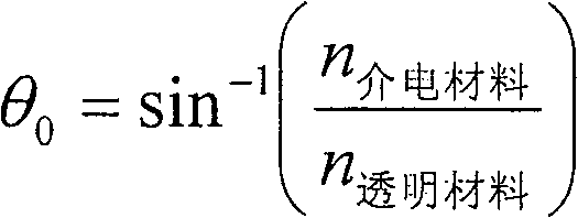
其中n介电材料是介电层122、132、142和152的材料的折射率,n透明材料是漏斗状光导管170a的透明材料的折射率。如果光子184的入射角θ大于临界角θ0,那么光子184将弹回(即,反射)到漏斗状光导管170a中。然后,光子184可沿着漏斗状光导管170a向下传播并到达光电二极管112a,或以可能不同的入射角(未示出)一次或多次撞击侧壁165a和169a。如果这些入射角也大于临界角θ0,那么光子184将沿着漏斗状光导管170a向下传播且到达光电二极管112a。n透明材料越大,临界角θ0就越小,因此到达光电二极管112a的绿色光子(像光子184)就越多。穿过蓝色CFA区域180b的光束的蓝色光子将以相似的方式沿着漏斗状光导管170b向下传播且到达光电二极管112b。穿过红色CFA区域180d的光束的红色光子将以相似的方式沿着漏斗状光导管170d向下传播且到达光电二极管112d。结果,n透明材料越大,到达光电二极管112a、112b、112c和112d的光束的光子就越多。应注意,以上描述是对于在侧壁165a、165b、165c、165d、169a、169b、169c和169d上没有光反射涂层的情况。如果漏斗状导管164a、168a;164b、168b;164c、168c和164d、168d的侧壁165a、165b、165c、165d、169a、169b、169c和169d被涂覆有光反射材料(如铝),然后参考图1H如上所述被填充有透明材料,则无论入射角θ如何,光子184将反射回来。Where ndielectric material is the refractive index of the material of the
图2示出了根据本发明实施例的像素传感器200的截面图。在一个实施例中,除了漏斗264a、264b、264c和264d的每个侧壁265a、265b、265c和265d的截面具有如图2所示的凸面双曲线的形状(分别与图1I所示的漏斗164a、164b、164c和164d的侧壁165a、165b、165c和165d的凹面双曲线相反)之外,该像素传感器200与图1I的像素传感器100相似。为简明起见,相似的区域和层将具有相同的参考标号。在一个实施例中,通过利用化学物质或另一化学物质的变化的组分的蚀刻来分别形成漏斗264a、264b、264c和264d的凸面双曲线的侧壁265a、265b、265c和265d。在一个实施例中,通过聚合RIE工艺(例如具有CHF3或C4F8的碳氟化合物的化学物质)形成漏斗264a、264b、264c和264d的凸面双曲线侧壁265a、265b、265c和265d,然后通过非聚合RIE工艺(CF4或CHF3/O2或C4F8/O2)形成光导管的下部。FIG. 2 shows a cross-sectional view of a
在一个实施例中,像素传感器200的操作与如上所述图1I的像素传感器100的操作相似。更具体地,当光束(未示出)入射到结构200的表面286上时,穿过CFA区域180a、180b、180c和180d的光束的大多数光子将分别到达光电二极管112a、112b、112c和112d。In one embodiment, the operation of
图3示出了根据本发明实施例的像素传感器300的截面图。在一个实施例中,除了漏斗364a、364b、364c和364d的每个侧壁365a、365b、365c和365d的截面是如图3所示的倾斜直线之外,像素传感器300与图1I的像素传感器100相似。在一个实施例中,通过利用化学物质或另一化学物质的变化的组分的蚀刻来分别形成漏斗364a、364b、364c和364d的直侧壁365a、365b、365c和365d。在一个实施例中,通过聚合RIE工艺(例如具有CHF3或C4F8的碳氟化合物的化学物质)形成直的漏斗364a、364b、364c和364d,然后通过非聚合RIE工艺(CF4或CHF3/O2或C4F8/O2)形成光导管的下部。在一个实施例中,也可通过各向异性的RIE以形成非锥形光导管(包括下部),随后通过溅射蚀刻(例如在Ar中)以形成光导管的锥形上部,形成直的漏斗364a、364b、364c和364d。FIG. 3 shows a cross-sectional view of a
在一个实施例中,像素传感器300的操作与如上所述的图1I的像素传感器100的操作相似。更具体地,当光束(未示出)入射到结构300的表面386上时,穿过CFA区域180a、180b、180c和180d的光束的大多数光子将分别到达光电二极管112a、112b、112c以及112d。In one embodiment, the operation of
图4示出了根据本发明实施例的像素传感器400的截面图。在一个实施例中,除了漏斗状光导管168a、480a;168b、480b;168c、480c和168d、480d的形成之外,像素传感器400的形成与图1H的结构100的形成相似。更具体地,利用透明材料填充漏斗状光导管168a、480a;168b、480b;168c、480c和168d、480d的空腔168a、168b、168c和168d,然后沿着被填充的空腔168a、168b、168c和168d向下回蚀刻该透明材料。接下来,在一个实施例中,通过利用任何常规方法,在漏斗164a、164b、164c和164d中分别形成CFA漏斗状区域480a、480b、480c和480d,得到图4的结构400。更具体地,用绿色滤光材料填充漏斗164a和164c以形成仅允许绿色光子穿过的绿色CFA漏斗状区域480a和480c。然后,用蓝色滤光材料填充漏斗164b以形成仅允许蓝色光子穿过的蓝色CFA漏斗状区域480b。然后,用红色滤光材料填充漏斗164d以形成仅允许红色光子穿过的红色CFA漏斗状区域480d。FIG. 4 shows a cross-sectional view of a
在一个实施例中,图4的像素传感器400的操作与图1I的像素传感器100的操作相似。应注意,CFA漏斗状区域480a、480b、480c和480d起两个作用:(a)滤色区域的作用(与图1I的CFA区域180a、180b、180c和180d的作用相似)以及(b)漏斗状区域的作用(与图1I的已被填充的漏斗164a、164b、164c和164d的作用相似)。In one embodiment, the operation of
图4’示出了根据本发明实施例的像素传感器400’的截面图。在一个实施例中,除了分别在CFA漏斗状区域480a、480b、480c和480d的顶部上形成微透镜490a 490b、490c和490d之外,像素传感器400′的形成与图4的像素传感器400的形成相似。微透镜490a、490b、490c和490d用于将光分别聚焦到CFA漏斗状区域480a、480b、480c和480d中。应注意,可将微透镜490a、490b、490c和490d应用到所有实施例,包括具有或不具有滤色阵列的实施例(像图1I的CFA区域180a、180b、180c和180d)。Figure 4' shows a cross-sectional view of a pixel sensor 400' according to an embodiment of the present invention. In one embodiment, the formation of pixel sensor 400' is similar to the formation of
在上述实施例中,参考图1A-1I,存在四个光电二极管112a、112b、112c以及112d。通常,像素传感器100可具有N个光电二极管,其中N是正整数。In the above embodiment, referring to FIGS. 1A-1I , there are four
在上述实施例中,参考图1E,蚀刻步骤162在互连层140的氮化物层146处停止。在可选实施例中,在将氮化物层146暴露于周围环境之前蚀刻步骤162停止。在另一可选实施例中,蚀刻步骤162蚀刻贯穿氮化物层146且在氮化物层136处停止。通常,蚀刻步骤162可在互连多层155中的任何位置处停止。In the embodiments described above, referring to FIG. 1E , the
在上述实施例中,漏斗164a、164b、164c和164d的侧壁(图1G),漏斗264a、264b、264c和264d的侧壁(图2),以及漏斗364a、364b、364c和364d的侧壁(图3)具有双曲线的形状。可选地,它们具有抛物线形状。In the above-described embodiment, the side walls of
虽然为了示例的目的在此描述了本发明的具体实施例,对于本领域技术人员来说,许多修改和改变将变得显而易见。因此,所附的权利要求旨在包括落入本发明的真实精神和范围内的所有这些修改和改变。Although specific embodiments of the invention have been described herein for illustrative purposes, many modifications and changes will become apparent to those skilled in the art. Accordingly, the appended claims are intended to cover all such modifications and changes as fall within the true spirit and scope of this invention.
Claims (25)
Applications Claiming Priority (2)
| Application Number | Priority Date | Filing Date | Title |
|---|---|---|---|
| US11/275,171 US7524694B2 (en) | 2005-12-16 | 2005-12-16 | Funneled light pipe for pixel sensors |
| US11/275,171 | 2005-12-16 |
Publications (2)
| Publication Number | Publication Date |
|---|---|
| CN1983610A CN1983610A (en) | 2007-06-20 |
| CN100536153C true CN100536153C (en) | 2009-09-02 |
Family
ID=36124628
Family Applications (1)
| Application Number | Title | Priority Date | Filing Date |
|---|---|---|---|
| CNB2006101641183A Active CN100536153C (en) | 2005-12-16 | 2006-11-14 | Pixel sensor structure and manufacturing method of semiconductor structure |
Country Status (2)
| Country | Link |
|---|---|
| US (1) | US7524694B2 (en) |
| CN (1) | CN100536153C (en) |
Cited By (1)
| Publication number | Priority date | Publication date | Assignee | Title |
|---|---|---|---|---|
| CN113687511A (en) * | 2020-05-19 | 2021-11-23 | 雅得近显股份有限公司 | Near-to-eye display device |
Families Citing this family (39)
| Publication number | Priority date | Publication date | Assignee | Title |
|---|---|---|---|---|
| US8029186B2 (en) * | 2004-11-05 | 2011-10-04 | International Business Machines Corporation | Method for thermal characterization under non-uniform heat load |
| US20080290435A1 (en) * | 2007-05-21 | 2008-11-27 | Micron Technology, Inc. | Wafer level lens arrays for image sensor packages and the like, image sensor packages, and related methods |
| US8890271B2 (en) | 2010-06-30 | 2014-11-18 | Zena Technologies, Inc. | Silicon nitride light pipes for image sensors |
| US20100304061A1 (en) * | 2009-05-26 | 2010-12-02 | Zena Technologies, Inc. | Fabrication of high aspect ratio features in a glass layer by etching |
| US20100148221A1 (en) * | 2008-11-13 | 2010-06-17 | Zena Technologies, Inc. | Vertical photogate (vpg) pixel structure with nanowires |
| US8889455B2 (en) * | 2009-12-08 | 2014-11-18 | Zena Technologies, Inc. | Manufacturing nanowire photo-detector grown on a back-side illuminated image sensor |
| US8835831B2 (en) | 2010-06-22 | 2014-09-16 | Zena Technologies, Inc. | Polarized light detecting device and fabrication methods of the same |
| US9515218B2 (en) * | 2008-09-04 | 2016-12-06 | Zena Technologies, Inc. | Vertical pillar structured photovoltaic devices with mirrors and optical claddings |
| US8229255B2 (en) * | 2008-09-04 | 2012-07-24 | Zena Technologies, Inc. | Optical waveguides in image sensors |
| US8735797B2 (en) | 2009-12-08 | 2014-05-27 | Zena Technologies, Inc. | Nanowire photo-detector grown on a back-side illuminated image sensor |
| US8274039B2 (en) | 2008-11-13 | 2012-09-25 | Zena Technologies, Inc. | Vertical waveguides with various functionality on integrated circuits |
| US20110115041A1 (en) * | 2009-11-19 | 2011-05-19 | Zena Technologies, Inc. | Nanowire core-shell light pipes |
| US9000353B2 (en) | 2010-06-22 | 2015-04-07 | President And Fellows Of Harvard College | Light absorption and filtering properties of vertically oriented semiconductor nano wires |
| US9406709B2 (en) | 2010-06-22 | 2016-08-02 | President And Fellows Of Harvard College | Methods for fabricating and using nanowires |
| US9478685B2 (en) | 2014-06-23 | 2016-10-25 | Zena Technologies, Inc. | Vertical pillar structured infrared detector and fabrication method for the same |
| US7646943B1 (en) | 2008-09-04 | 2010-01-12 | Zena Technologies, Inc. | Optical waveguides in image sensors |
| US8546742B2 (en) * | 2009-06-04 | 2013-10-01 | Zena Technologies, Inc. | Array of nanowires in a single cavity with anti-reflective coating on substrate |
| US8866065B2 (en) | 2010-12-13 | 2014-10-21 | Zena Technologies, Inc. | Nanowire arrays comprising fluorescent nanowires |
| US8507840B2 (en) | 2010-12-21 | 2013-08-13 | Zena Technologies, Inc. | Vertically structured passive pixel arrays and methods for fabricating the same |
| US8269985B2 (en) | 2009-05-26 | 2012-09-18 | Zena Technologies, Inc. | Determination of optimal diameters for nanowires |
| US9343490B2 (en) | 2013-08-09 | 2016-05-17 | Zena Technologies, Inc. | Nanowire structured color filter arrays and fabrication method of the same |
| US8299472B2 (en) | 2009-12-08 | 2012-10-30 | Young-June Yu | Active pixel sensor with nanowire structured photodetectors |
| US9082673B2 (en) | 2009-10-05 | 2015-07-14 | Zena Technologies, Inc. | Passivated upstanding nanostructures and methods of making the same |
| US8748799B2 (en) | 2010-12-14 | 2014-06-10 | Zena Technologies, Inc. | Full color single pixel including doublet or quadruplet si nanowires for image sensors |
| US9299866B2 (en) | 2010-12-30 | 2016-03-29 | Zena Technologies, Inc. | Nanowire array based solar energy harvesting device |
| US8791470B2 (en) | 2009-10-05 | 2014-07-29 | Zena Technologies, Inc. | Nano structured LEDs |
| US8384007B2 (en) * | 2009-10-07 | 2013-02-26 | Zena Technologies, Inc. | Nano wire based passive pixel image sensor |
| US8519379B2 (en) | 2009-12-08 | 2013-08-27 | Zena Technologies, Inc. | Nanowire structured photodiode with a surrounding epitaxially grown P or N layer |
| US8324010B2 (en) | 2010-06-29 | 2012-12-04 | Himax Imaging, Inc. | Light pipe etch control for CMOS fabrication |
| US20120018831A1 (en) * | 2010-07-20 | 2012-01-26 | Himax Imaging, Inc. | Light pipe fabrication with improved sensitivity |
| US9093579B2 (en) * | 2011-04-28 | 2015-07-28 | Semiconductor Components Industries, Llc | Dielectric barriers for pixel arrays |
| CN102279456B (en) * | 2011-06-29 | 2013-09-11 | 中海阳新能源电力股份有限公司 | Light gathering power transmission one body type integration relay system |
| US8680454B2 (en) * | 2011-12-01 | 2014-03-25 | Omnivision Technologies, Inc. | Backside-illuminated (BSI) pixel including light guide |
| TW201616552A (en) * | 2014-10-24 | 2016-05-01 | 力晶科技股份有限公司 | Semiconductor process method |
| TWI572024B (en) * | 2015-07-06 | 2017-02-21 | 力晶科技股份有限公司 | Semiconductor component and method of manufacturing same |
| US10302774B2 (en) * | 2016-04-25 | 2019-05-28 | Morpho Detection, Llc | Detector assembly for use in CT imaging systems |
| US10192917B2 (en) | 2016-06-30 | 2019-01-29 | Stmicroelectronics (Crolles 2) Sas | Backside illuminated photosensor element with light pipe and light mirror structures |
| US10585238B2 (en) * | 2017-06-13 | 2020-03-10 | The University Of North Carolina At Charlotte | Photodetector focal plane array systems and methods based on microcomponents with arbitrary shapes |
| US10608036B2 (en) * | 2017-10-17 | 2020-03-31 | Qualcomm Incorporated | Metal mesh light pipe for transporting light in an image sensor |
Family Cites Families (16)
| Publication number | Priority date | Publication date | Assignee | Title |
|---|---|---|---|---|
| US3110816A (en) * | 1960-09-20 | 1963-11-12 | Westinghouse Electric Corp | High resolution light pipe radiation detector |
| US3727057A (en) | 1962-06-15 | 1973-04-10 | Westinghouse Electric Corp | Infrared detector device with a mosaic of oppositely-poled adjacent elements |
| US4495220A (en) * | 1983-10-07 | 1985-01-22 | Trw Inc. | Polyimide inter-metal dielectric process |
| US5352886A (en) * | 1993-03-30 | 1994-10-04 | The United States Of America As Represented By The Secretary Of The Air Force | Micro non-imaging light concentrators for image sensors with a lenslet array |
| JP3674209B2 (en) * | 1997-01-23 | 2005-07-20 | ソニー株式会社 | Solid-state imaging device and manufacturing method thereof |
| JP2001304973A (en) * | 2000-04-26 | 2001-10-31 | Denso Corp | Infrared image sensor |
| GB2369724B (en) * | 2000-12-04 | 2003-04-30 | Infrared Integrated Syst Ltd | Improving individual detector performance in radiation detector arrays |
| US6912330B2 (en) | 2001-05-17 | 2005-06-28 | Sioptical Inc. | Integrated optical/electronic circuits and associated methods of simultaneous generation thereof |
| JP2003197897A (en) | 2001-12-28 | 2003-07-11 | Fuji Film Microdevices Co Ltd | Semiconductor photoelectric transducer |
| US7061028B2 (en) * | 2003-03-12 | 2006-06-13 | Taiwan Semiconductor Manufacturing, Co., Ltd. | Image sensor device and method to form image sensor device |
| JP4123060B2 (en) * | 2003-06-11 | 2008-07-23 | ソニー株式会社 | Solid-state imaging device and manufacturing method thereof |
| JP2005251804A (en) * | 2004-03-01 | 2005-09-15 | Canon Inc | Image sensor |
| US7119319B2 (en) * | 2004-04-08 | 2006-10-10 | Canon Kabushiki Kaisha | Solid-state image sensing element and its design support method, and image sensing device |
| US7704778B2 (en) * | 2005-02-23 | 2010-04-27 | Taiwan Semiconductor Manufacturing Company, Ltd. | Microlens structure for image sensors |
| US20070187787A1 (en) * | 2006-02-16 | 2007-08-16 | Ackerson Kristin M | Pixel sensor structure including light pipe and method for fabrication thereof |
| US7358583B2 (en) * | 2006-02-24 | 2008-04-15 | Tower Semiconductor Ltd. | Via wave guide with curved light concentrator for image sensing devices |
-
2005
- 2005-12-16 US US11/275,171 patent/US7524694B2/en active Active
-
2006
- 2006-11-14 CN CNB2006101641183A patent/CN100536153C/en active Active
Cited By (1)
| Publication number | Priority date | Publication date | Assignee | Title |
|---|---|---|---|---|
| CN113687511A (en) * | 2020-05-19 | 2021-11-23 | 雅得近显股份有限公司 | Near-to-eye display device |
Also Published As
| Publication number | Publication date |
|---|---|
| US7524694B2 (en) | 2009-04-28 |
| CN1983610A (en) | 2007-06-20 |
| US20070138380A1 (en) | 2007-06-21 |
Similar Documents
| Publication | Publication Date | Title |
|---|---|---|
| CN100536153C (en) | Pixel sensor structure and manufacturing method of semiconductor structure | |
| US11699718B2 (en) | Semiconductor image sensor | |
| TWI677993B (en) | Semiconductor device and method of forming an image sensor integrated chip | |
| US8716771B2 (en) | Anti-reflection structures for CMOS image sensors | |
| KR102278324B1 (en) | Semiconductor image sensor | |
| US8003425B2 (en) | Methods for forming anti-reflection structures for CMOS image sensors | |
| TWI608600B (en) | Image sensor and manufacturing method thereof | |
| KR102288339B1 (en) | Semiconductor image sensor | |
| TWI623090B (en) | Backside photosensitive image sensor and forming method thereof | |
| US20100203665A1 (en) | Methods of manufacturing an image sensor having an air gap | |
| CN101971340A (en) | image sensing reflector | |
| JP6505180B2 (en) | Method of manufacturing solid-state imaging device having flat microlens | |
| TW202119645A (en) | Image sensor, integrated chip, and method of forming image sensor | |
| CN106158891B (en) | For improving the stacking grid design of optical property and isolation | |
| JP2021061330A (en) | Solid state imaging device and manufacturing method thereof | |
| TWI793543B (en) | Integrated chip with composite deep trench isolation structure and method of forming the same | |
| KR102486685B1 (en) | Enhanced design for image sensing technology | |
| JP2008141014A (en) | Pixel sensor structure and method for manufacturing semiconductor structure (funnel-shaped optical pipe for pixel sensor) | |
| TW202236646A (en) | Backside illuminated image sensor and manufacturing method therefore | |
| CN107958913A (en) | Image sensor and manufacturing method thereof | |
| TWI707465B (en) | Image sensing device and method of forming the same |
Legal Events
| Date | Code | Title | Description |
|---|---|---|---|
| C06 | Publication | ||
| PB01 | Publication | ||
| C10 | Entry into substantive examination | ||
| SE01 | Entry into force of request for substantive examination | ||
| C14 | Grant of patent or utility model | ||
| GR01 | Patent grant | ||
| TR01 | Transfer of patent right | ||
| TR01 | Transfer of patent right |
Effective date of registration: 20180822 Address after: Cayman Islands Patentee after: SmartSens Technology (Cayman) Co.,Ltd. Address before: American New York Patentee before: International Business Machines Corp. |
|
| TR01 | Transfer of patent right | ||
| TR01 | Transfer of patent right |
Effective date of registration: 20200702 Address after: Room 612, 6th floor, No. 111 Building, Xiangke Road, China (Shanghai) Free Trade Pilot Area, Pudong New Area, Shanghai Patentee after: Siteway (Shanghai) Electronic Technology Co.,Ltd. Address before: Cayman Islands Patentee before: SmartSens Technology (Cayman) Co.,Ltd. |
|
| CP01 | Change in the name or title of a patent holder | ||
| CP01 | Change in the name or title of a patent holder |
Address after: Room 612, 6th floor, No. 111 Building, Xiangke Road, China (Shanghai) Free Trade Pilot Area, Pudong New Area, Shanghai, 201203 Patentee after: Starway (Shanghai) Electronic Technology Co.,Ltd. Address before: Room 612, 6th floor, No. 111 Building, Xiangke Road, China (Shanghai) Free Trade Pilot Area, Pudong New Area, Shanghai, 201203 Patentee before: Siteway (Shanghai) Electronic Technology Co.,Ltd. |