CN100535713C - Liquid crystal display device and driving method thereof - Google Patents
Liquid crystal display device and driving method thereof Download PDFInfo
- Publication number
- CN100535713C CN100535713C CNB2006100872725A CN200610087272A CN100535713C CN 100535713 C CN100535713 C CN 100535713C CN B2006100872725 A CNB2006100872725 A CN B2006100872725A CN 200610087272 A CN200610087272 A CN 200610087272A CN 100535713 C CN100535713 C CN 100535713C
- Authority
- CN
- China
- Prior art keywords
- pattern
- polysilicon semiconductor
- drain
- region
- gate
- Prior art date
- Legal status (The legal status is an assumption and is not a legal conclusion. Google has not performed a legal analysis and makes no representation as to the accuracy of the status listed.)
- Expired - Fee Related
Links
Images


Classifications
-
- G—PHYSICS
- G02—OPTICS
- G02F—OPTICAL DEVICES OR ARRANGEMENTS FOR THE CONTROL OF LIGHT BY MODIFICATION OF THE OPTICAL PROPERTIES OF THE MEDIA OF THE ELEMENTS INVOLVED THEREIN; NON-LINEAR OPTICS; FREQUENCY-CHANGING OF LIGHT; OPTICAL LOGIC ELEMENTS; OPTICAL ANALOGUE/DIGITAL CONVERTERS
- G02F1/00—Devices or arrangements for the control of the intensity, colour, phase, polarisation or direction of light arriving from an independent light source, e.g. switching, gating or modulating; Non-linear optics
- G02F1/01—Devices or arrangements for the control of the intensity, colour, phase, polarisation or direction of light arriving from an independent light source, e.g. switching, gating or modulating; Non-linear optics for the control of the intensity, phase, polarisation or colour
- G02F1/13—Devices or arrangements for the control of the intensity, colour, phase, polarisation or direction of light arriving from an independent light source, e.g. switching, gating or modulating; Non-linear optics for the control of the intensity, phase, polarisation or colour based on liquid crystals, e.g. single liquid crystal display cells
- G02F1/133—Constructional arrangements; Operation of liquid crystal cells; Circuit arrangements
- G02F1/1333—Constructional arrangements; Manufacturing methods
- G02F1/1345—Conductors connecting electrodes to cell terminals
- G02F1/13454—Drivers integrated on the active matrix substrate
-
- G—PHYSICS
- G02—OPTICS
- G02F—OPTICAL DEVICES OR ARRANGEMENTS FOR THE CONTROL OF LIGHT BY MODIFICATION OF THE OPTICAL PROPERTIES OF THE MEDIA OF THE ELEMENTS INVOLVED THEREIN; NON-LINEAR OPTICS; FREQUENCY-CHANGING OF LIGHT; OPTICAL LOGIC ELEMENTS; OPTICAL ANALOGUE/DIGITAL CONVERTERS
- G02F1/00—Devices or arrangements for the control of the intensity, colour, phase, polarisation or direction of light arriving from an independent light source, e.g. switching, gating or modulating; Non-linear optics
- G02F1/01—Devices or arrangements for the control of the intensity, colour, phase, polarisation or direction of light arriving from an independent light source, e.g. switching, gating or modulating; Non-linear optics for the control of the intensity, phase, polarisation or colour
- G02F1/13—Devices or arrangements for the control of the intensity, colour, phase, polarisation or direction of light arriving from an independent light source, e.g. switching, gating or modulating; Non-linear optics for the control of the intensity, phase, polarisation or colour based on liquid crystals, e.g. single liquid crystal display cells
- G02F1/133—Constructional arrangements; Operation of liquid crystal cells; Circuit arrangements
- G02F1/136—Liquid crystal cells structurally associated with a semi-conducting layer or substrate, e.g. cells forming part of an integrated circuit
-
- H—ELECTRICITY
- H10—SEMICONDUCTOR DEVICES; ELECTRIC SOLID-STATE DEVICES NOT OTHERWISE PROVIDED FOR
- H10D—INORGANIC ELECTRIC SEMICONDUCTOR DEVICES
- H10D84/00—Integrated devices formed in or on semiconductor substrates that comprise only semiconducting layers, e.g. on Si wafers or on GaAs-on-Si wafers
- H10D84/01—Manufacture or treatment
- H10D84/0123—Integrating together multiple components covered by H10D12/00 or H10D30/00, e.g. integrating multiple IGBTs
- H10D84/0126—Integrating together multiple components covered by H10D12/00 or H10D30/00, e.g. integrating multiple IGBTs the components including insulated gates, e.g. IGFETs
- H10D84/0165—Integrating together multiple components covered by H10D12/00 or H10D30/00, e.g. integrating multiple IGBTs the components including insulated gates, e.g. IGFETs the components including complementary IGFETs, e.g. CMOS devices
- H10D84/017—Manufacturing their source or drain regions, e.g. silicided source or drain regions
-
- G—PHYSICS
- G02—OPTICS
- G02F—OPTICAL DEVICES OR ARRANGEMENTS FOR THE CONTROL OF LIGHT BY MODIFICATION OF THE OPTICAL PROPERTIES OF THE MEDIA OF THE ELEMENTS INVOLVED THEREIN; NON-LINEAR OPTICS; FREQUENCY-CHANGING OF LIGHT; OPTICAL LOGIC ELEMENTS; OPTICAL ANALOGUE/DIGITAL CONVERTERS
- G02F1/00—Devices or arrangements for the control of the intensity, colour, phase, polarisation or direction of light arriving from an independent light source, e.g. switching, gating or modulating; Non-linear optics
- G02F1/01—Devices or arrangements for the control of the intensity, colour, phase, polarisation or direction of light arriving from an independent light source, e.g. switching, gating or modulating; Non-linear optics for the control of the intensity, phase, polarisation or colour
- G02F1/13—Devices or arrangements for the control of the intensity, colour, phase, polarisation or direction of light arriving from an independent light source, e.g. switching, gating or modulating; Non-linear optics for the control of the intensity, phase, polarisation or colour based on liquid crystals, e.g. single liquid crystal display cells
- G02F1/133—Constructional arrangements; Operation of liquid crystal cells; Circuit arrangements
- G02F1/136—Liquid crystal cells structurally associated with a semi-conducting layer or substrate, e.g. cells forming part of an integrated circuit
- G02F1/1362—Active matrix addressed cells
- G02F1/136227—Through-hole connection of the pixel electrode to the active element through an insulation layer
-
- G—PHYSICS
- G02—OPTICS
- G02F—OPTICAL DEVICES OR ARRANGEMENTS FOR THE CONTROL OF LIGHT BY MODIFICATION OF THE OPTICAL PROPERTIES OF THE MEDIA OF THE ELEMENTS INVOLVED THEREIN; NON-LINEAR OPTICS; FREQUENCY-CHANGING OF LIGHT; OPTICAL LOGIC ELEMENTS; OPTICAL ANALOGUE/DIGITAL CONVERTERS
- G02F1/00—Devices or arrangements for the control of the intensity, colour, phase, polarisation or direction of light arriving from an independent light source, e.g. switching, gating or modulating; Non-linear optics
- G02F1/01—Devices or arrangements for the control of the intensity, colour, phase, polarisation or direction of light arriving from an independent light source, e.g. switching, gating or modulating; Non-linear optics for the control of the intensity, phase, polarisation or colour
- G02F1/13—Devices or arrangements for the control of the intensity, colour, phase, polarisation or direction of light arriving from an independent light source, e.g. switching, gating or modulating; Non-linear optics for the control of the intensity, phase, polarisation or colour based on liquid crystals, e.g. single liquid crystal display cells
- G02F1/133—Constructional arrangements; Operation of liquid crystal cells; Circuit arrangements
- G02F1/136—Liquid crystal cells structurally associated with a semi-conducting layer or substrate, e.g. cells forming part of an integrated circuit
- G02F1/1362—Active matrix addressed cells
- G02F1/1368—Active matrix addressed cells in which the switching element is a three-electrode device
-
- H—ELECTRICITY
- H10—SEMICONDUCTOR DEVICES; ELECTRIC SOLID-STATE DEVICES NOT OTHERWISE PROVIDED FOR
- H10D—INORGANIC ELECTRIC SEMICONDUCTOR DEVICES
- H10D84/00—Integrated devices formed in or on semiconductor substrates that comprise only semiconducting layers, e.g. on Si wafers or on GaAs-on-Si wafers
- H10D84/01—Manufacture or treatment
- H10D84/02—Manufacture or treatment characterised by using material-based technologies
- H10D84/03—Manufacture or treatment characterised by using material-based technologies using Group IV technology, e.g. silicon technology or silicon-carbide [SiC] technology
- H10D84/038—Manufacture or treatment characterised by using material-based technologies using Group IV technology, e.g. silicon technology or silicon-carbide [SiC] technology using silicon technology, e.g. SiGe
-
- G—PHYSICS
- G02—OPTICS
- G02F—OPTICAL DEVICES OR ARRANGEMENTS FOR THE CONTROL OF LIGHT BY MODIFICATION OF THE OPTICAL PROPERTIES OF THE MEDIA OF THE ELEMENTS INVOLVED THEREIN; NON-LINEAR OPTICS; FREQUENCY-CHANGING OF LIGHT; OPTICAL LOGIC ELEMENTS; OPTICAL ANALOGUE/DIGITAL CONVERTERS
- G02F1/00—Devices or arrangements for the control of the intensity, colour, phase, polarisation or direction of light arriving from an independent light source, e.g. switching, gating or modulating; Non-linear optics
- G02F1/01—Devices or arrangements for the control of the intensity, colour, phase, polarisation or direction of light arriving from an independent light source, e.g. switching, gating or modulating; Non-linear optics for the control of the intensity, phase, polarisation or colour
- G02F1/13—Devices or arrangements for the control of the intensity, colour, phase, polarisation or direction of light arriving from an independent light source, e.g. switching, gating or modulating; Non-linear optics for the control of the intensity, phase, polarisation or colour based on liquid crystals, e.g. single liquid crystal display cells
- G02F1/133—Constructional arrangements; Operation of liquid crystal cells; Circuit arrangements
- G02F1/136—Liquid crystal cells structurally associated with a semi-conducting layer or substrate, e.g. cells forming part of an integrated circuit
- G02F1/1362—Active matrix addressed cells
- G02F1/136213—Storage capacitors associated with the pixel electrode
-
- G—PHYSICS
- G02—OPTICS
- G02F—OPTICAL DEVICES OR ARRANGEMENTS FOR THE CONTROL OF LIGHT BY MODIFICATION OF THE OPTICAL PROPERTIES OF THE MEDIA OF THE ELEMENTS INVOLVED THEREIN; NON-LINEAR OPTICS; FREQUENCY-CHANGING OF LIGHT; OPTICAL LOGIC ELEMENTS; OPTICAL ANALOGUE/DIGITAL CONVERTERS
- G02F1/00—Devices or arrangements for the control of the intensity, colour, phase, polarisation or direction of light arriving from an independent light source, e.g. switching, gating or modulating; Non-linear optics
- G02F1/01—Devices or arrangements for the control of the intensity, colour, phase, polarisation or direction of light arriving from an independent light source, e.g. switching, gating or modulating; Non-linear optics for the control of the intensity, phase, polarisation or colour
- G02F1/13—Devices or arrangements for the control of the intensity, colour, phase, polarisation or direction of light arriving from an independent light source, e.g. switching, gating or modulating; Non-linear optics for the control of the intensity, phase, polarisation or colour based on liquid crystals, e.g. single liquid crystal display cells
- G02F1/133—Constructional arrangements; Operation of liquid crystal cells; Circuit arrangements
- G02F1/136—Liquid crystal cells structurally associated with a semi-conducting layer or substrate, e.g. cells forming part of an integrated circuit
- G02F1/1362—Active matrix addressed cells
- G02F1/136218—Shield electrodes
-
- G—PHYSICS
- G02—OPTICS
- G02F—OPTICAL DEVICES OR ARRANGEMENTS FOR THE CONTROL OF LIGHT BY MODIFICATION OF THE OPTICAL PROPERTIES OF THE MEDIA OF THE ELEMENTS INVOLVED THEREIN; NON-LINEAR OPTICS; FREQUENCY-CHANGING OF LIGHT; OPTICAL LOGIC ELEMENTS; OPTICAL ANALOGUE/DIGITAL CONVERTERS
- G02F1/00—Devices or arrangements for the control of the intensity, colour, phase, polarisation or direction of light arriving from an independent light source, e.g. switching, gating or modulating; Non-linear optics
- G02F1/01—Devices or arrangements for the control of the intensity, colour, phase, polarisation or direction of light arriving from an independent light source, e.g. switching, gating or modulating; Non-linear optics for the control of the intensity, phase, polarisation or colour
- G02F1/13—Devices or arrangements for the control of the intensity, colour, phase, polarisation or direction of light arriving from an independent light source, e.g. switching, gating or modulating; Non-linear optics for the control of the intensity, phase, polarisation or colour based on liquid crystals, e.g. single liquid crystal display cells
- G02F1/133—Constructional arrangements; Operation of liquid crystal cells; Circuit arrangements
- G02F1/136—Liquid crystal cells structurally associated with a semi-conducting layer or substrate, e.g. cells forming part of an integrated circuit
- G02F1/1362—Active matrix addressed cells
- G02F1/136286—Wiring, e.g. gate line, drain line
- G02F1/13629—Multilayer wirings
-
- G—PHYSICS
- G02—OPTICS
- G02F—OPTICAL DEVICES OR ARRANGEMENTS FOR THE CONTROL OF LIGHT BY MODIFICATION OF THE OPTICAL PROPERTIES OF THE MEDIA OF THE ELEMENTS INVOLVED THEREIN; NON-LINEAR OPTICS; FREQUENCY-CHANGING OF LIGHT; OPTICAL LOGIC ELEMENTS; OPTICAL ANALOGUE/DIGITAL CONVERTERS
- G02F2202/00—Materials and properties
- G02F2202/10—Materials and properties semiconductor
- G02F2202/104—Materials and properties semiconductor poly-Si
Landscapes
- Physics & Mathematics (AREA)
- Nonlinear Science (AREA)
- Mathematical Physics (AREA)
- Chemical & Material Sciences (AREA)
- Crystallography & Structural Chemistry (AREA)
- General Physics & Mathematics (AREA)
- Optics & Photonics (AREA)
- Engineering & Computer Science (AREA)
- Microelectronics & Electronic Packaging (AREA)
- Liquid Crystal (AREA)
- Thin Film Transistor (AREA)
- Devices For Indicating Variable Information By Combining Individual Elements (AREA)
- Internal Circuitry In Semiconductor Integrated Circuit Devices (AREA)
Abstract
Description
本发明要求2005年11月9日在韩国提交的韩国专利申请第10-2005-0106839号的优先权,在此引入其全部内容作为参考。This application claims priority from Korean Patent Application No. 10-2005-0106839 filed in Korea on Nov. 9, 2005, the entire contents of which are hereby incorporated by reference.
技术领域 technical field
本发明涉及一种液晶显示器件,尤其涉及一种液晶显示器件及其制造方法。The invention relates to a liquid crystal display device, in particular to a liquid crystal display device and a manufacturing method thereof.
背景技术 Background technique
近年来,显示器件一般使用阴极射线管(CRT)。目前,正在努力研究和发展作为CRT替代品的各种类型的平板显示器,如液晶显示(LCD)器件、等离子体显示面板(PDP)、场发射显示器(FED)、和电致发光显示器(ELD)。具体地说,这些类型的平板显示器件以有源矩阵型显示驱动,在有源矩阵型显示中利用其中的多个薄膜晶体管驱动以矩阵形式排列的多个像素。在有源矩阵型平板显示中,液晶显示(LCD)器件和电致发光显示(ELD)器件由于其高分辨率、显示色彩的能力以及在显示运动图像方面的优越性而广泛用于笔记本计算机和台式计算机。In recent years, cathode ray tubes (CRTs) have generally been used as display devices. Currently, efforts are being made to research and develop various types of flat panel displays as a substitute for CRTs, such as liquid crystal display (LCD) devices, plasma display panels (PDP), field emission displays (FED), and electroluminescent displays (ELD) . Specifically, these types of flat panel display devices are driven by an active matrix type display in which a plurality of thin film transistors therein are used to drive a plurality of pixels arranged in a matrix. Among active matrix flat panel displays, liquid crystal display (LCD) devices and electroluminescent display (ELD) devices are widely used in notebook computers and desktop computer.
一般地,LCD器件包括彼此间隔并面对的矩阵基板和彩色滤色片基板,在两个基板之间夹入液晶材料。两个基板包括彼此面对的电极从而在电极之间施加的电压产生液晶材料的电场。液晶材料中液晶分子的排列根据产生的电场强度而在产生的电场方向上改变,由此改变LCD器件的光透射率。因而,LCD器件通过改变产生的电场强度显示图像。In general, an LCD device includes a matrix substrate and a color filter substrate spaced apart from and facing each other, with a liquid crystal material sandwiched between the two substrates. The two substrates include electrodes facing each other such that a voltage applied between the electrodes generates an electric field of the liquid crystal material. The alignment of liquid crystal molecules in the liquid crystal material changes in the direction of the generated electric field according to the strength of the generated electric field, thereby changing the light transmittance of the LCD device. Thus, the LCD device displays images by changing the strength of the generated electric field.
近年来,使用有源矩阵型LCD器件,其中薄膜晶体管以矩阵方式设置在阵列基板上。多晶硅或多晶硅用作薄膜晶体管的半导体层。当使用氢化多晶硅(a-Si:H)时,可使用较低的温度处理,因而可使用较低价格的基板。然而,因为氢化多晶硅具有较差的电场特性,如0.1到1.0cm2/Vs的迁移率,所以很难使用氢化多晶硅形成直接在阵列基板上的驱动电路。多晶硅具有比氢化多晶硅高的迁移率。因此,当使用多晶硅时,可在阵列基板上很容易地直接形成驱动电路,且液晶显示面板具有紧凑的尺寸。In recent years, an active matrix type LCD device is used in which thin film transistors are arranged in a matrix on an array substrate. Polysilicon or polysilicon is used as the semiconductor layer of the thin film transistor. When using hydrogenated polysilicon (a-Si:H), lower temperature processing can be used and thus lower priced substrates can be used. However, since hydrogenated polysilicon has poor electric field characteristics, such as a mobility of 0.1 to 1.0 cm 2 /Vs, it is difficult to form a driving circuit directly on an array substrate using hydrogenated polysilicon. Polysilicon has a higher mobility than hydrogenated polysilicon. Therefore, when polysilicon is used, a driving circuit can be easily directly formed on the array substrate, and the liquid crystal display panel has a compact size.
图1是依照现有技术的LCD器件阵列基板的示意性平面图。FIG. 1 is a schematic plan view of an LCD device array substrate according to the prior art.
如图1中所示,在基板10中确定了显示区域D1和非显示区域D2。在显示区域D1中,多条栅线12和多条数据线14设置在基板10上并彼此交叉从而确定多个像素区域P。在每个像素区域P中,设置有像素薄膜晶体管T和像素电极17。像素薄膜晶体管T是n-型或p-型。As shown in FIG. 1 , a display area D1 and a non-display area D2 are defined in the
在非显示区域D2中,在基板10上设置有栅驱动电路16和数据驱动电路18。栅驱动电路16设置在基板10的一侧并给栅线12供给栅信号,数据驱动电路18设置在基板10的另一侧并给数据线14供给数据信号。栅和数据驱动电路16和18包括CMOS(互补金属氧化物半导体)器件,其具有n-型驱动晶体管和p-型驱动薄膜晶体管。In the non-display area D2 , a
图2是图1中LCD器件的阵列基板显示区域的平面图。FIG. 2 is a plan view of an array substrate display area of the LCD device in FIG. 1 .
如图2中所示,在基板30上,栅线GL沿着第一方向延伸,数据线DL沿着第二方向延伸。栅线GL和数据线DL彼此交叉以确定像素区域P。存储线SL沿阵第一方向延伸并与栅线GL间隔开。As shown in FIG. 2, on the
像素薄膜晶体管T设置在栅线和数据线GL和DL的交叉部分处。像素薄膜晶体管T包括栅极52、多晶硅半导体图案38、源极74a和漏极74b。像素电极82设置在像素区域P中并与漏极74b接触。在像素区域P中设置有包含第一,第二和第三存储电极40,54和76的存储电容器Cst。The pixel thin film transistor T is disposed at a crossing portion of the gate and data lines GL and DL. The pixel thin film transistor T includes a
图3A是图1中LCD器件的一部分驱动电路的截面图,图3B是沿图2的线III-III提取的截面图。3A is a cross-sectional view of a part of a driving circuit of the LCD device in FIG. 1, and FIG. 3B is a cross-sectional view taken along line III-III of FIG.
如图3A和3B中所示,非显示区域D2中的驱动电路(栅或数据驱动电路)DC包括CMOS器件,CMOS器件包括p-型驱动薄膜晶体管T(p)和n-型驱动薄膜晶体管T(n)。As shown in FIGS. 3A and 3B, the drive circuit (gate or data drive circuit) DC in the non-display area D2 includes a CMOS device, and the CMOS device includes a p-type drive thin film transistor T (p) and an n-type drive thin film transistor T (n).
在显示区域D1的像素区域P中,设置有与像素薄膜晶体管Ts接触的像素电极82和像素存储电容器Cst。像素薄膜晶体管Ts是n-型或p-型薄膜晶体管,n-型薄膜晶体管主要用作像素薄膜晶体管Ts。像素存储电容器Cst包括第一,第二和第三存储电极40,54和76。像素存储电容器Cst包括第一存储电容器C1和第二存储电容器C2。In the pixel region P of the display region D1, a
图4A到4I所示为在现有技术阵列基板非显示区域的制造工序中的截面图,图5A到5I所示为在现有技术阵列基板显示区域的制造工序中的截面图,图6A到6I是分别沿图5A到5I的线III-III提取的截面图。4A to 4I show cross-sectional views in the manufacturing process of the non-display area of the array substrate in the prior art, and FIGS. 5A to 5I show cross-sectional views in the manufacturing process of the display area of the array substrate in the prior art, and FIGS. 6I is a sectional view taken along line III-III of FIGS. 5A to 5I, respectively.
如图4A,5A和6A中所示,在具有显示区域D1和非显示区域D2的基板30上形成缓冲层32。显示区域D1具有像素区域P、开关区域A3和存储区域A4,非显示区域D2具有p-型区域A1和n-型区域A2。在缓冲层32上沉积氢化多晶硅(a-Si:H)并结晶。以第一掩模工序将结晶的硅(多晶硅)层构图,从而在p-型区域A1、n-型区域A2、开关区域A3和存储区域A4中分别形成第一,第二,第三和第四多晶硅半导体图案34,36,38和40。第三和第四多晶硅图案38和40形成为一体。As shown in FIGS. 4A, 5A and 6A, a
如图4B,5B和6B中所示,在具有多晶硅半导体图案34,36,38和40上沉积光刻胶并以第二掩模工序构图,从而形成光刻胶图案42。光刻胶图案42覆盖了p-型区域A1、n-型区域A2和开关区域A3。对第四多晶硅半导体图案40执行使用n+离子的离子掺杂工序。通过掺杂工序,减小了第四多晶硅半导体图案40的电阻。在掺杂工序之后,移除光刻胶图案42。掺杂的第四多晶硅半导体图案40是第一存储电极40。As shown in FIGS. 4B , 5B and 6B, photoresist is deposited on the
如图4C,5C和6C中所示,在具有第一存储电极40的基板30上形成栅绝缘层46。在栅绝缘层46上沉积金属材料层并以第三掩模工序构图,从而形成第一到第三栅极48,50和52以及第二存储电极54。第一到第三栅极48,50和52分别对应于第一到第三多晶硅半导体图案34,36和38的中部,第二存储电极54对应于第一存储电极40。在第三掩模工序中,还形成了栅线GL和存储线SL。As shown in FIGS. 4C , 5C and 6C, a
如图4D,5D和6D中所示,在第四掩模工序中,在具有栅极48,50和52的基板30上沉积光刻胶并进行构图,从而形成光刻胶图案56。光刻胶图案56覆盖了p-型区域A1。对n-型区域A2和开关区域A3执行使用n+离子的离子掺杂工序。用n+离子掺杂第二和第三多晶硅半导体图案36和38的侧部。第二和第三多晶硅半导体图案36和38的离子掺杂的侧部具有欧姆接触特性。然后移除光刻胶图案56。As shown in FIGS. 4D , 5D and 6D , in a fourth masking process, a photoresist is deposited and patterned on the
如图4E,5E和6E中所示,在第五掩模工序中,在完成了n+掺杂工序的基板30上沉积光刻胶并进行构图,从而形成光刻胶图案58。光刻胶图案58覆盖n-型区域A2、开关区域A3和存储区域A4。对p-型区域A1执行使用p+离子的离子掺杂工序。用p+离子掺杂第一多晶硅半导体图案34的侧部。第一多晶硅半导体图案34的离子掺杂的侧部具有欧姆接触特性。然后移除光刻胶图案58。As shown in FIGS. 4E , 5E and 6E , in the fifth mask process, a photoresist is deposited and patterned on the
如图4F,5F和6F中所示,在其中完成了p+掺杂工序的基板30上形成层间绝缘膜60。在第六掩模工序中,对栅绝缘层46和层间绝缘膜60进行构图,从而形成暴露第一多晶硅半导体图案34的离子掺杂部分的第一和第二接触孔62a和62b、暴露第二多晶硅半导体图案36的离子掺杂部分的第三和第四接触孔64a和64b、和暴露第三多晶硅半导体图案38的离子掺杂部分的第五和第六接触孔66a和66b。As shown in FIGS. 4F, 5F and 6F, an
如图4G,5G和6G中所示,在第七掩模工序中,在钝化层60上沉积金属材料并构图,从而形成与第一多晶硅半导体图案34的离子掺杂部分接触的第一源极和漏极70a和70b、与第二多晶硅半导体图案36的离子掺杂部分接触的第二源极和漏极72a和72b、和与第三多晶硅半导体图案38的离子掺杂部分接触的第三源极和漏极74a和74b。同时形成数据线DL,并在存储区域A4中形成从第三漏极74b延伸的第三存储电极76。As shown in FIGS. 4G, 5G and 6G, in the seventh mask process, a metal material is deposited and patterned on the
通过上面的第一到第七掩模工序,在非显示区域D2中形成具有n-型驱动薄膜晶体管和p-型驱动薄膜晶体管的CMOS。在显示区域D1的开关区域A3中形成n-型像素薄膜晶体管,并且形成了包括由第一和第二电极40和54形成的第一存储电容器C1和由第二和第三电极54和76形成的第二存储电容器C2的像素存储电容器。Through the above first to seventh mask processes, a CMOS having an n-type driving thin film transistor and a p-type driving thin film transistor is formed in the non-display region D2. An n-type pixel thin film transistor is formed in the switching area A3 of the display area D1, and a first storage capacitor C1 formed by the first and
如图4H,5H和6H中所示,在具有数据线DL的基板30上形成钝化层78。在第八掩模工序中,对钝化层78进行构图,从而形成暴露第三存储电极76(或第三漏极74b)的漏极接触孔80。As shown in FIGS. 4H, 5H and 6H, a
如图4I,5I和6I中所示,在第九掩模工序中,在钝化层78上沉积透明导电材料并构图,从而形成像素电极82。像素电极82通过漏极接触孔(图6H中的80)与第三漏极74b连接。As shown in FIGS. 4I , 5I and 6I, in a ninth mask process, a transparent conductive material is deposited and patterned on the
通过上面的第一到第九掩模工序,制造了其上直接形成有驱动电路的现有的阵列基板。随着掩模工序增加,产品成本也增加,且生产率降低了。因此需要减小掩模工序。Through the above first to ninth mask processes, a conventional array substrate on which a driving circuit is directly formed is manufactured. As the mask process increases, product cost also increases, and productivity decreases. Therefore, it is necessary to reduce the mask process.
发明内容 Contents of the invention
液晶显示器件包括在基板非显示区域中的p-型驱动薄膜晶体管和n-型驱动薄膜晶体管。该p-型驱动薄膜晶体管包括第一多晶硅半导体图案、第一栅极、第一源极和第一漏极。该n-型驱动薄膜晶体管包括第二多晶硅半导体图案、第二栅极、第二源极和第二漏极。液晶显示器件进一步包括在基板显示区域中彼此交叉确定像素区域的栅线和数据线、和与栅线和数据线连接的像素驱动薄膜晶体管。该像素薄膜晶体管包括第三多晶硅半导体图案、第三栅极、第三源极和第三漏极。液晶显示器件进一步包括覆盖并直接接触第三漏极的像素电极、覆盖并直接接触第一源极和第一漏极、第二源极和第二漏极每一个的遮光图案、和覆盖并直接接触数据线和第三源极的遮光线。A liquid crystal display device includes a p-type driving thin film transistor and an n-type driving thin film transistor in a non-display area of a substrate. The p-type driving thin film transistor includes a first polysilicon semiconductor pattern, a first gate, a first source and a first drain. The n-type driving thin film transistor includes a second polysilicon semiconductor pattern, a second gate, a second source and a second drain. The liquid crystal display device further includes gate lines and data lines crossing each other to define pixel areas in the display area of the substrate, and pixel driving thin film transistors connected to the gate lines and the data lines. The pixel thin film transistor includes a third polysilicon semiconductor pattern, a third gate, a third source and a third drain. The liquid crystal display device further includes a pixel electrode covering and directly contacting the third drain, a light-shielding pattern covering and directly contacting each of the first source and the first drain, the second source and the second drain, and covering and directly contacting each of the first source and the first drain, the second source and the second drain. The shielding line that contacts the data line and the third source.
在另一个方面中,一种制造液晶显示器件的方法包括:在基板非显示区域的p-型和n-型区域中分别形成第一和第二多晶硅半导体图案、在基板显示区域的开关区域和存储区域中分别形成第三和第四多晶硅半导体图案、在第四多晶硅半导体图案上形成存储图案。第四多晶硅半导体图案从第三多晶硅图案延伸。一种制造液晶显示器件的方法进一步包括在第一到第四多晶硅半导体图案上形成栅绝缘层,在栅绝缘层上方,在p-型区域中形成第一栅极、在n-型区域中形成第一金属图案、在开关区域和存储区域中形成第二金属图案、形成与第二金属图案连接的栅线。一种制造液晶显示器件的方法进一步包括在形成第一栅极和第一和第二金属图案后用p+离子掺杂第一多晶硅半导体图案的第一源部和漏部,由n-型区域中的第一金属图案形成第二栅极,由开关区域和存储区域中的第二金属图案分别形成第三栅极和第二存储电极。一种制造液晶显示器件的方法进一步包括在形成第二和第三栅极以及第二存储电极之后用n+离子掺杂第二多晶硅半导体图案的第二源极和漏极部以及第三多晶硅半导体图案的第三源极和漏极部,在第一到第三栅极和第二存储电极上形成层间绝缘膜,形成层间绝缘膜的接触孔,其暴露第一源部和漏部、第二源部和漏部、第三源部的每一个以及第三漏部、第四多晶硅半导体图案和存储图案之一。该制造液晶显示器件的方法进一步包括在n-型区域、p-型区域和开关区域的每一个中都形成源极和漏极、在存储区域中形成第二存储电极、在层间绝缘膜上形成与开关区域的源极连接的数据线,在开关区域的漏极和第三存储电极上形成像素电极、在n-型区域和p-型区域的源极和漏极上形成遮光图案、在数据线和开关区域的源极上形成遮光线,其中第一存储电极包括所述存储图案和第四多晶硅半导体图案。In another aspect, a method of manufacturing a liquid crystal display device includes: respectively forming first and second polysilicon semiconductor patterns in p-type and n-type regions of a non-display region of a substrate, a switch in a display region of a substrate Third and fourth polysilicon semiconductor patterns are respectively formed in the area and the storage area, and a storage pattern is formed on the fourth polysilicon semiconductor pattern. The fourth polysilicon semiconductor pattern extends from the third polysilicon pattern. A method of manufacturing a liquid crystal display device further includes forming a gate insulating layer on the first to fourth polysilicon semiconductor patterns, forming a first gate in the p-type region, forming a first gate in the n-type region over the gate insulating layer A first metal pattern is formed in the first metal pattern, a second metal pattern is formed in the switch area and the storage area, and a gate line connected to the second metal pattern is formed. A method of manufacturing a liquid crystal display device further includes doping the first source portion and the drain portion of the first polysilicon semiconductor pattern with p+ ions after forming the first gate and the first and second metal patterns, by n-type The first metal pattern in the area forms a second gate, and the second metal pattern in the switch area and the storage area form a third gate and a second storage electrode, respectively. A method of manufacturing a liquid crystal display device further includes doping the second source and drain portions and the third polysilicon semiconductor pattern with n+ ions after forming the second and third gate electrodes and the second storage electrode. The third source and drain portions of the crystalline silicon semiconductor pattern, an interlayer insulating film is formed on the first to third gates and the second storage electrode, and a contact hole of the interlayer insulating film is formed, which exposes the first source portion and the second storage electrode. Each of the drain, the second source and the drain, the third source, and the third drain, one of the fourth polysilicon semiconductor pattern and the memory pattern. The method of manufacturing a liquid crystal display device further includes forming a source electrode and a drain electrode in each of the n-type region, the p-type region, and the switch region, forming a second storage electrode in the storage region, forming a second storage electrode on the interlayer insulating film Form a data line connected to the source of the switch region, form a pixel electrode on the drain of the switch region and the third storage electrode, form a light-shielding pattern on the source and drain of the n-type region and the p-type region, and A shielding line is formed on the data line and the source electrode of the switch region, wherein the first storage electrode includes the storage pattern and the fourth polysilicon semiconductor pattern.
在另一个方面中,液晶显示器件包括:在基板非显示区域中的p-型驱动薄膜晶体管和n-型驱动薄膜晶体管以及在基板显示区域中的像素薄膜晶体管。p-型、n-型和像素薄膜晶体管每一个都包括多晶硅半导体图案、在多晶硅半导体图案上的栅极、和栅极上的源极和漏极。液晶显示器件进一步包括在多晶硅半导体图案和栅极之间的栅绝缘层、在栅极与源极和漏极之间的层间绝缘膜、和彼此交叉从而确定显示区域的像素区域的栅线和数据线。液晶显示器件进一步包括像素区域中的像素电极、和与像素薄膜晶体管连接的存储电容器。存储电容器包括第一存储电极,其具有从像素薄膜晶体管延伸的多晶硅半导体图案延伸的存储多晶硅半导体图案和在存储多晶硅半导体图案正上方的存储图案、在栅绝缘层上的第二存储电极、和从像素薄膜晶体管的漏极延伸的第三存储电极。In another aspect, a liquid crystal display device includes: a p-type driving thin film transistor and an n-type driving thin film transistor in a non-display area of a substrate and a pixel thin film transistor in a display area of the substrate. Each of the p-type, n-type and pixel thin film transistors includes a polysilicon semiconductor pattern, a gate on the polysilicon semiconductor pattern, and a source and a drain on the gate. The liquid crystal display device further includes a gate insulating layer between the polysilicon semiconductor pattern and the gate, an interlayer insulating film between the gate and the source and drain electrodes, and gate lines and pixel regions crossing each other to define a display region. data line. The liquid crystal display device further includes a pixel electrode in the pixel area, and a storage capacitor connected to the pixel thin film transistor. The storage capacitor includes a first storage electrode having a storage polysilicon semiconductor pattern extending from a polysilicon semiconductor pattern extending from the pixel thin film transistor and a storage pattern directly above the storage polysilicon semiconductor pattern, a second storage electrode on the gate insulating layer, and The drain of the pixel TFT extends from the third storage electrode.
应当理解,前面一般的描述和下面详细的描述都是示范性的和解释性的,意在提供如权利要求所述的本发明的进一步解释。It is to be understood that both the foregoing general description and the following detailed description are exemplary and explanatory and are intended to provide further explanation of the invention as claimed.
附图说明 Description of drawings
所附附图用于对发明作进一步说明并作为本说明书的一部分,其阐述了本发明的实施方式并与附图说明结合以用于解释本发明的原理。The accompanying drawings are used to further illustrate the invention and are a part of this specification, which illustrate the implementation of the present invention and are combined with the description of the drawings to explain the principles of the present invention.
图1所示为依照现有技术的LCD器件阵列基板的示意性平面图;FIG. 1 is a schematic plan view of an LCD device array substrate according to the prior art;
图2所示为图1中LCD器件阵列基板的显示区域的平面图;FIG. 2 is a plan view of the display area of the LCD device array substrate in FIG. 1;
图3A所示为图1中LCD器件的一部分驱动电路的截面图;FIG. 3A is a cross-sectional view of a part of the driving circuit of the LCD device in FIG. 1;
图3B所示为沿图2的线II-II提取的截面图;Figure 3B is a cross-sectional view taken along line II-II of Figure 2;
图4A到4I所示为在现有技术阵列基板的非显示区域的制造工序中的截面图;4A to 4I are cross-sectional views in the manufacturing process of the non-display area of the prior art array substrate;
图5A到5I所示为在现有技术阵列基板的显示区域的制造工序中的平面图;5A to 5I are plan views in the manufacturing process of the display region of the prior art array substrate;
图6A到6I所示为分别沿图5A到5I的线III-III提取的截面图;Figures 6A to 6I are cross-sectional views taken along line III-III of Figures 5A to 5I, respectively;
图7所示为依照本发明示例性实施方式的LCD器件阵列基板的显示区域的平面图;7 is a plan view showing a display area of an LCD device array substrate according to an exemplary embodiment of the present invention;
图8A所示为依照本发明示例性实施方式的LCD器件阵列基板的驱动电路的非显示区域的截面图;8A is a cross-sectional view of a non-display area of a driving circuit of an LCD device array substrate according to an exemplary embodiment of the present invention;
图8B所示为沿图7的线V-V提取的截面图;Figure 8B shows a cross-sectional view taken along the line V-V of Figure 7;
图9A到9N所示为在依照本发明示例性实施方式的阵列基板的非显示区域制造工序中的截面图;9A to 9N are cross-sectional views showing a non-display region manufacturing process of an array substrate according to an exemplary embodiment of the present invention;
图10A到10N所示为在依照本发明示例性实施方式的阵列基板的显示区域制造工序中的平面图;以及10A to 10N are plan views showing a display region manufacturing process of an array substrate according to an exemplary embodiment of the present invention; and
图11A到11N所示为分别沿图10A到10N的线V-V的截面图。11A to 11N are cross-sectional views taken along line V-V of FIGS. 10A to 10N, respectively.
具体实施方式 Detailed ways
现在将详细描述本发明的优选实施方式,在附图中示出了其实施例。Reference will now be made in detail to the preferred embodiments of the invention, examples of which are illustrated in the accompanying drawings.
图7是依照本发明示例性实施方式的LCD器件阵列基板的显示区域的平面图。7 is a plan view of a display area of an array substrate of an LCD device according to an exemplary embodiment of the present invention.
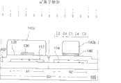
如图7中所示,在基板100上,栅线GL沿第一方向延伸,数据线DL沿第二方向延伸。栅线GL和数据线DL彼此交叉以确定像素区域P。存储线SL与栅线GL间隔开并沿第一方向延伸。As shown in FIG. 7, on the
像素薄膜晶体管设置在栅线GL和数据线DL的交叉部分处。像素薄膜晶体管包括栅极148、多晶硅半导体图案116、源极164a和漏极164b。The pixel thin film transistor is disposed at a crossing portion of the gate line GL and the data line DL. The pixel thin film transistor includes a
像素电极170设置在像素区域P中并不需要通过接触孔而是直接与漏极164b接触。The
在像素区域P中设置有包括第一,第二和第三存储电极S1,150和166的存储电容器Cst。第一存储电极S1具有从多晶硅半导体图案116延伸的存储部118和存储图案124。第二存储电极150从存储线SL延伸。第三存储电极166从漏极164b延伸。In the pixel region P, a storage capacitor Cst including first, second and third storage electrodes S1, 150 and 166 is disposed. The first storage electrode S1 has a
像素电极170覆盖了漏极164b和第三存储电极166。以与像素电极170相同的层设置遮光线173,其覆盖数据线DL和源极164a。The
图8A是依照本发明示例性实施方式的LCD器件阵列基板的驱动电路的非显示区域的截面图,图8B是沿图7的线V-V提取的截面图。8A is a cross-sectional view of a non-display area of a driving circuit of an LCD device array substrate according to an exemplary embodiment of the present invention, and FIG. 8B is a cross-sectional view taken along line V-V of FIG. 7 .
如图8A和8B中所示,阵列基板包括显示区域D1和非显示区域D2。非显示区域D2中的驱动电路(栅或数据驱动电路)包括CMOS器件,CMOS器件包括在p-型区域A1中的p-型驱动薄膜晶体管,在n-型区域中的n-型驱动薄膜晶体管。P-型驱动薄膜晶体管包括第一栅极136、第一多晶硅半导体图案112和第一源极和漏极160a和160b。n-型驱动薄膜晶体管包括第二栅极146、第二多晶硅半导体图案114和第二源极和漏极162a和162b。遮光图案172设置在每第一源极和漏极160a和160b以及第二源极和漏极162a和162b每一个的正上方并将它们覆盖。As shown in FIGS. 8A and 8B, the array substrate includes a display area D1 and a non-display area D2. The driving circuit (gate or data driving circuit) in the non-display area D2 includes a CMOS device, and the CMOS device includes a p-type driving thin film transistor in the p-type area A1, an n-type driving thin film transistor in the n-type area . The P-type driving thin film transistor includes a
在显示区域D1的像素区域P中,设置有像素薄膜晶体管、像素电极170和像素存储电容器。像素薄膜晶体管设置在开关区域A3中并包括第三栅极148、第三多晶硅半导体图案116和第三源极和漏极164a和164b。遮光线173在数据线(图7的DL)和第三源极164a正上方并将它们覆盖。像素电极170设置在像素区域P中并在漏极164b和第三存储电极166正上方且将它们覆盖。In the pixel region P of the display region D1, a pixel thin film transistor, a
像素存储电容器设置在存储区域A4中并包括第一和第二存储电容器C1和C2。第一和第二存储电极S1和150形成了第一存储电容器C1,第二和第三存储电极150和166形成了第二存储电容器C2。第一和第二存储电容器C1和C2并联。第一存储电极S1包括第四多晶硅半导体图案118和第四多晶硅半导体图案118上的存储图案124。第四多晶硅半导体图案118与第三多晶硅半导体图案116一体形成。第三存储电极166也与第三漏极164b一体形成。The pixel storage capacitor is disposed in the storage area A4 and includes first and second storage capacitors C1 and C2. The first and second storage electrodes S1 and 150 form a first storage capacitor C1, and the second and
层间绝缘膜包括两层,第一层152a由硅的氧化物(SiO2)形成,第二层152b由硅的氮化物(SiNx)形成。由硅的氮化物(SiNx)形成的第二层152b与像素电极170接触。The interlayer insulating film includes two layers, the
图9A到9N所示为在依照本发明示例性实施方式的阵列基板的非显示区域制造工序中的截面图,图10A到10N所示为在依照本发明示例性实施方式的阵列基板的显示区域制造工序中的平面图,图11A到11N分别是沿图10A到10N的线V-V提取的截面图。9A to 9N are cross-sectional views showing the non-display area manufacturing process of the array substrate according to the exemplary embodiment of the present invention, and FIGS. 10A to 10N are the display area of the array substrate according to the exemplary embodiment of the present invention. As plan views in the manufacturing process, FIGS. 11A to 11N are cross-sectional views taken along line V-V in FIGS. 10A to 10N , respectively.
如图9A,10A和11A中所示,在具有显示区域D1和非显示区域D2的基板100上形成缓冲层102、多晶硅层104和第一金属层106。非显示区域D2具有p-型区域A1和n-型区域A2,显示区域D1具有像素区域P、开关区域A3和存储区域A4。As shown in FIGS. 9A, 10A and 11A, a
缓冲层102由包括硅的氮化物(SiNx)和硅的氧化物(SiO2)的无机绝缘材料形成。多晶硅层104可通过沉积、脱氢和结晶氢化多晶硅(a-Si:H)形成。第一金属层106包括钨(W)、钼(Mo)、铬(Cr)和钼-钨(MoW)。The
在第一金属层106上形成第一光刻胶层108。在第一光刻胶层108上方设置第一掩模M。第一掩模M包括透射部M1、遮挡部M2和半透射部M3。半透射部M3透射具有比遮挡部M2大并小于透射部M1的量的光,半透射部M3具有半透射膜或狭缝结构。A
掩模M1设置为遮挡部M2对应于存储区域A4,半透射部M3对应于p-型区域A1、n-型区域A2和开关区域A3,透射部M1对应于上面的区域A1到A4之外的其它区域。对应于开关区域A3的半透射部M3和对应于存储区域A4的遮挡部M1彼此相邻。The mask M1 is set such that the shielding part M2 corresponds to the storage area A4, the semi-transmissive part M3 corresponds to the p-type region A1, the n-type region A2 and the switch region A3, and the transmissive part M1 corresponds to the areas outside the upper regions A1 to A4. other areas. The semi-transmissive part M3 corresponding to the switching area A3 and the blocking part M1 corresponding to the storage area A4 are adjacent to each other.
使用掩模M将第一光刻胶层108曝光。假设第一光刻胶层108是p-型,其中曝光的部分被显影,而没有曝光的部分保留下来。Using a mask M, the
如图9B,10B和11B中所示,将用第一掩模(图9A和11A的M)曝光的第一光刻胶层(图9A,10A和11A的108)显影,从而形成第一到第三光刻胶图案110a,110b和110c。因为n-型和p-型区域A1和A2对应于半透射部(图9A的M3),所以第一和第二光刻胶图案110a和110b具有比第一光刻胶层低的高度。因为对应于开关区域A3的半透射部(图11A的M3)和对应于存储区域A4的遮挡部(图11A的M1)彼此相邻,所以开关区域A3中的一部分第三光刻胶图案110c具有比存储区域A4中的一部分第三光刻胶图案110c低的高度。第三光刻胶图案110c在开关区域A3和存储区域A4之间具有台阶。As shown in Figures 9B, 10B and 11B, the first photoresist layer (108 of Figures 9A, 10A and 11A) exposed with the first mask (M of Figures 9A and 11A) is developed to form the first to The
使用第一到第三光刻胶图案110a,110b和110c作为蚀刻掩模蚀刻第一金属层106和多晶硅层104。The
如图9C,10C和11C中所示,通过蚀刻工序,在第一光刻胶图案110a下方形成第一金属图案120和第一多晶硅半导体图案112,在第二光刻胶图案110b下方形成第二金属图案122和第二多晶硅半导体图案114,在第三光刻胶图案110c下方一体形成第三金属图案124以及第三和第四多晶硅半导体图案116和118。对于第一到第三光刻胶图案110a到110c执行灰化工序。As shown in FIGS. 9C, 10C and 11C, through an etching process, the
如图9D,10D和11D中所示,通过灰化工序,完全移除了第一和第二光刻胶图案(图9C的110a和110b),还完全移除了对应于开关区域A3的第三光刻胶图案110c部分,并部分移除了对应于存储区域A的第三光刻胶图案110c部分。As shown in FIGS. 9D, 10D and 11D, through the ashing process, the first and second photoresist patterns (110a and 110b in FIG. 9C) are completely removed, and the first and second photoresist patterns corresponding to the switch region A3 are also completely removed. A portion of the
使用灰化的第三光刻胶图案110c作为蚀刻掩模蚀刻第一到第三金属图案120,122和124。The first to
如图9E,10E和11E中所示,通过灰化工序,移除第一和第二金属图案(图9D的120和122)和对应于开关区域A3的第三金属图案124的部分,并且保留对应于存储区域A4的第三金属图案124的部分。蚀刻后的第三金属图案124是存储图案124。As shown in FIGS. 9E, 10E and 11E, through the ashing process, the first and second metal patterns (120 and 122 of FIG. 9D ) and the portion of the
通过上述的第一掩模工序,分别在p-型和n-型区域A1和A2中形成了第一和第二多晶硅半导体图案112和114。分别在开关区域A3和存储区域A4中一体形成了第三和第四多晶硅半导体图案116和118。在第四多晶硅半导体图案118上形成了存储图案124。因为在第四多晶硅半导体图案118上形成有存储图案124,所以不需要像现有技术一样使用第四多晶硅半导体图案118作为存储电极的单独掺杂工序。存储图案124和第四多晶硅半导体图案组成了第一存储电极(图8B的S1)。Through the first mask process described above, the first and second
如图9F,10F和11F中所示,在具有第一存储电极的基板110上形成栅绝缘层128。在栅绝缘层128上形成第二金属层130。第二金属层130包括铬(Cr)、钼(Mo)、钨(W)、铜(Cu)和铝合金(AlNd)。在第二金属层130上形成第二光刻胶层132。使用第二掩模(没有示出)对第二光刻胶层132执行包括曝光工序和显影工序的光刻工序。As shown in FIGS. 9F, 10F and 11F, a
如图9G,10G和11G中所示,通过光刻工序,形成了第一到第三光刻胶图案134a到134c。第一光刻胶图案134a对应于第一多晶硅半导体图案112的中部。第二光刻胶图案134b覆盖第二多晶硅半导体图案114。第三光刻胶图案134c覆盖第三和第四多晶硅半导体图案116和118。As shown in FIGS. 9G, 10G and 11G, through a photolithography process, first to third photoresist patterns 134a to 134c are formed. The first photoresist pattern 134 a corresponds to the middle of the first
使用第一到第三光刻胶图案134a到134c作为蚀刻掩模蚀刻第二金属层(图9F,10F和11F的130),从而形成第一栅极136和第一和第二金属图案138和140。Using the first to third photoresist patterns 134a to 134c as an etching mask to etch the second metal layer (130 of FIGS. 9F, 10F and 11F), thereby forming the
参照图10G,第三光刻胶图案134c不仅形成在第三和第四多晶硅半导体图案116和118上而且还形成在其中形成有栅线GL和存储线SL的区域中。因此,以与形成第一栅极136和第一和第二金属图案138和140相同的工序形成栅线GL和存储线SL。Referring to FIG. 10G, a
第一多晶硅半导体图案112具有对应于第一栅极136的第一沟道部B1、在第一沟道部B1两侧的第一源极和漏极部B2和B3。第一沟道部B1被第一栅极136覆盖,第一源极和漏极部B2和B3没有被第一栅极136覆盖。第一金属图案138覆盖第二多晶硅半导体图案114,第二金属图案140覆盖第三和第四多晶硅半导体图案116和118。然后移除第一到第三光刻胶图案134a到134c。The first
如图9H,10H和11H中所示,执行使用p+离子的离子掺杂工序。第一栅极136和第一和第二金属图案138和140用作掺杂掩模。不掺杂第一沟道部B1,而是掺杂第一源部和漏部B2和B3。掺杂的第一源部和漏部B2和B3具有欧姆接触特性。As shown in FIGS. 9H, 10H and 11H, an ion doping process using p+ ions is performed. The
如图9I,10I和11I中所示,在具有第一栅极136的基板100上形成第三光刻胶层。使用第三掩模(没有示出)对第三光刻胶层执行光刻工序。通过光刻工序,形成了第一到第四光刻胶图案142a到142d。第一光刻胶图案142a覆盖第一多晶硅半导体图案112。第二光刻胶图案142b对应于第二多晶硅半导体图案114的中部。第三光刻胶图案142c对应于第三多晶硅半导体图案116的中部。第三光刻胶图案142c还形成在栅线GL上。第四光刻胶图案142d形成在存储区域A4中。第四光刻胶图案142d还形成在存储线SL上。As shown in FIGS. 9I , 10I and 11I, a third photoresist layer is formed on the
使用第一到第四光刻胶图案142a到142d作为蚀刻掩模蚀刻第一和第二金属图案(图9H,10H和11H的138和140),从而形成第二和第三栅极146和148以及第二存储电极150。The first and second metal patterns (138 and 140 of FIGS. 9H, 10H and 11H) are etched using the first to
第二多晶硅半导体图案114具有第二沟道部C1、在第二沟道部C1两侧的第二源极和漏极部C2和C3、和第二沟道部C1与第二源极和漏极部C2和C3之间的第一轻掺杂漏极(LDD)部C4。第二沟道部C1和第一LDD部C4被第二栅极146覆盖,第二源极和漏极部C2和C3没有被第二栅极146覆盖。The second
第三多晶硅半导体图案116具有第三沟道部D1、在第三沟道部D1两侧的第三源极和漏极部D2和D3、和第三沟道部D1与第三源极和漏极部D2和D3之间的第二轻掺杂漏极(LDD)部D4。第三沟道部D1和第二LDD部D4被第三栅极148覆盖,第三源极和漏极部D2和D3没有被第三栅极148覆盖。The third
第二存储电极150与第三栅极148分离并从存储线SL延伸。第二存储电极150面对第一存储电极。The
当第一到第四光刻胶图案142a到142d保留时执行使用n+离子的离子掺杂工序。第二和第三沟道部C1和D1以及第一和第二LDD部C4和D4没有被掺杂,第二和第三源极部C2和D2以及第二和第三漏极部C3和D3被掺杂了。被掺杂的第二和第三源极部C2和D2以及第二和第三漏极部C3和D3具有欧姆接触特性。The ion doping process using n+ ions is performed while the first to
参照图10I,一部分(较低的部分)第四多晶硅半导体图案118没有被存储图案124和第二存储电极150覆盖。特别地,通过图11C到11E的灰化和蚀刻工序,移除了存储图案124的外部,存储图案124没有覆盖第四多晶硅半导体图案118的外部。在第四多晶硅半导体图案118的轮廓内设置有存储图案124的轮廓。在第四多晶硅半导体图案118的外部中,还有一些部分没有被第二存储电极150覆盖。因此,用n+离子掺杂该些部分(较低的部分)。Referring to FIG. 10I , a portion (lower portion) of the fourth
如图9J,10J和11J中所示,对第一到第四光刻胶图案142a到142d执行灰化工序。通过灰化工序,部分移除了第一到第四光刻胶图案142a到142d。更详细地,灰化工序执行到第二和第三光刻胶图案142b和142c的端部分别与第二和第三沟道部C1和D1相一致为止。分别暴露对应于第一和第二LDD部的第二和第三栅极146和148的侧部。部分移除第一和第四光刻胶图案142a和142d的侧部。第一光刻胶图案142将覆盖第一栅极136。暴露第二存储电极150、栅线GL和存储线S1的侧部。As shown in FIGS. 9J, 10J, and 11J, an ashing process is performed on the first to
蚀刻工序执行为移除第二和第三栅极146和148、第二存储电极150、栅线GL和存储线SL的暴露的侧部。蚀刻后的第二和第三栅极146和148分别对应于第二和第三沟道部C1和D1。The etching process is performed to remove exposed side portions of the second and
如图9K,10K和11K中所示,当灰化的第一到第四光刻胶图案142a到142d保留时执行使用n-离子的离子掺杂工序。用n-离子掺杂第一和第二LDD部C4和D4。n-离子的剂量小于p+离子和n+离子的剂量。第二源部和漏部C2和C3以及第三源部和漏部D2和D3不受n-离子掺杂的影响。第二和第三沟道部C1和D1没有被n-离子掺杂。由于形成了LDD部C4和D4,所以由于热电效应引起的泄漏电流被最小化。然后移除第一到第四光刻胶图案142a到142d。As shown in FIGS. 9K, 10K, and 11K, an ion doping process using n- ions is performed while the ashed first to
通过上面所述的第二和第三掩模工序,形成第一到第三栅极136,146和148,用p+,n+和n-离子掺杂第一到第三多晶硅半导体图案112,114和116,并形成第二存储电极150。Through the second and third mask processes described above, the first to
如图9L,10L和11L中所示,在具有第一到第三栅极136,146和148的基板100上形成层间绝缘膜152。层间绝缘膜152具有由硅的氧化物(SiO2)形成的第一层152a和由硅的氮化物(SiNx)形成的第二层152b。As shown in FIGS. 9L , 10L and 11L, an
在层间绝缘膜152上形成第四光刻胶层。使用第四掩模将层间绝缘膜152构图,从而形成第一到第六接触孔154a,154b,156a,156b,158a和158b。通过第一和第二接触孔154a和154b分别暴露第一源部和漏部(图9H的B2和B3)。通过第三和第四接触孔156a和156b分别暴露第二源部和漏部(图9J的C2和C3)。通过第五和第六接触孔158a和158b分别暴露第三源部和漏部(图11J的D2和D3)。A fourth photoresist layer is formed on the
在形成接触孔154a,154b,156a,156b,158a和158b后,执行热处理。通过热处理,如上面所述在第四多晶硅半导体图案118的一些部分处掺杂的n+离子向着存储电极124下面扩散。在存储图案124和第四多晶硅半导体图案118之间形成欧姆接触,其中扩散了n+离子,因而存储图案124和n+离子扩散的第四多晶硅半导体部118电连接。After forming the
因为第三和第四多晶硅半导体图案116和118一体形成且第四多晶硅半导体图案118具有欧姆接触特性,所以第六接触孔158b可形成在存储图案124外部的第四多晶硅半导体图案118上或形成在存储图案124上。Since the third and fourth
如图9M,10M和11M中所示,在层间绝缘膜152上形成第三金属层并使用第五掩模构图,从而形成第一源极和漏极160a和160b、第二源极和漏极162a和162b、第三源极和漏极164a和164b以及第三存储电极166。第三存储电极166从第三漏极164b延伸,第三存储电极166和第三漏极164b一体形成。在形成源极和漏极160a,160b,162a,162b,164a和164b以及第三存储电极166的同时形成数据线DL。第三金属层包括铬(Cr)、钼(Mo)、钨(W)、铜(Cu)和铝合金(AlNd)。As shown in FIGS. 9M, 10M and 11M, a third metal layer is formed on the
如图9N,10N和11N中所示,在具有源极和漏极160a,160b,162a,162b,164a和164b以及第三存储电极166的基板100上形成透明导电材料层。透明导电材料包括氧化铟锡(ITO)、氧化铟锌(IZO)和氧化铟锡锌(ITZO)。使用第六掩模将透明导电材料层构图,从而在像素区域P中形成像素电极170。As shown in FIGS. 9N , 10N and 11N , a transparent conductive material layer is formed on the
像素电极170完全覆盖并直接接触第三漏极164b和第三存储电极166。像素电极170还直接与层间绝缘膜152接触。在形成像素电极170的同时形成遮光图案172和遮光线173。遮光图案172完全覆盖并直接接触每一个第一源极和漏极160a和160b以及第二源极和漏极162a和162b。遮光线173完全覆盖并直接接触数据线DL和第三源极164a。The
透明导电材料层的蚀刻溶液通过与透明导电材料层下面的金属图案DL,160a,160b,162a,162b,164a,164b和166反应可产生电化现象。为了阻止该问题,像素电极170、遮光图案172和遮光线173完全覆盖下面的金属图案DL,160a,160b,162a,162b,164a,164b和166。像素电极170直接接触层间绝缘膜152的第二层152b。因为第二层152b由硅的氮化物(SiNx)形成,所以层间绝缘膜152和像素电极170的界面特性很好,像素电极170的电阻不会增加。The etching solution of the transparent conductive material layer may generate an electrochemical phenomenon by reacting with the metal patterns DL, 160a, 160b, 162a, 162b, 164a, 164b and 166 under the transparent conductive material layer. In order to prevent this problem, the
通过上述的六个掩模工序,制造了示例性实施方式的LCD器件的阵列基板。尽管图中没有示出,但可通过形成与每个像素区域对应的彩色滤色片层、与栅极和数据线对应的黑矩阵、和面对像素电极的公共电极可制造面对阵列基板的彩色滤色片基板。将阵列基板和彩色滤色片基板粘附并在阵列基板和彩色滤色片基板之间填充液晶层,从而制造了LCD。Through the six masking processes described above, the array substrate of the LCD device of the exemplary embodiment is manufactured. Although not shown in the figure, the array substrate facing array substrate can be manufactured by forming a color filter layer corresponding to each pixel area, a black matrix corresponding to the gate and data lines, and a common electrode facing the pixel electrode. Color filter substrate. The LCD is manufactured by adhering the array substrate and the color filter substrate and filling the liquid crystal layer between the array substrate and the color filter substrate.
通过比现有技术少的掩模工序可制造依照示例性实施方式的阵列基板。减小了产品成本且生产率提高了。The array substrate according to example embodiments may be manufactured through fewer masking processes than the related art. Product cost is reduced and productivity is increased.
在不脱离本发明精神或范围的情况下本发明的液晶显示器件以及制造液晶显示器件的方法可以做各种修改和变化,这对于本领域熟练技术人员来说是显而易见的。因而本发明意在覆盖落入所附权利要求及其等效物范围内的本发明的修改和变化。It will be apparent to those skilled in the art that various modifications and changes can be made in the liquid crystal display device and the method of manufacturing the liquid crystal display device of the present invention without departing from the spirit or scope of the present invention. Thus, it is intended that the present invention covers the modifications and variations of this invention that come within the scope of the appended claims and their equivalents.
Claims (23)
Applications Claiming Priority (2)
| Application Number | Priority Date | Filing Date | Title |
|---|---|---|---|
| KR1020050106839A KR20070049742A (en) | 2005-11-09 | 2005-11-09 | An array substrate of lcd and method of fabricating of the same |
| KR1020050106839 | 2005-11-09 |
Related Child Applications (1)
| Application Number | Title | Priority Date | Filing Date |
|---|---|---|---|
| CN2009101594735A Division CN101614921B (en) | 2005-11-09 | 2006-06-14 | Liquid crystal display device and method of fabricating the same |
Publications (2)
| Publication Number | Publication Date |
|---|---|
| CN1963602A CN1963602A (en) | 2007-05-16 |
| CN100535713C true CN100535713C (en) | 2009-09-02 |
Family
ID=38003366
Family Applications (2)
| Application Number | Title | Priority Date | Filing Date |
|---|---|---|---|
| CNB2006100872725A Expired - Fee Related CN100535713C (en) | 2005-11-09 | 2006-06-14 | Liquid crystal display device and driving method thereof |
| CN2009101594735A Expired - Fee Related CN101614921B (en) | 2005-11-09 | 2006-06-14 | Liquid crystal display device and method of fabricating the same |
Family Applications After (1)
| Application Number | Title | Priority Date | Filing Date |
|---|---|---|---|
| CN2009101594735A Expired - Fee Related CN101614921B (en) | 2005-11-09 | 2006-06-14 | Liquid crystal display device and method of fabricating the same |
Country Status (4)
| Country | Link |
|---|---|
| US (2) | US8289491B2 (en) |
| JP (1) | JP4580368B2 (en) |
| KR (1) | KR20070049742A (en) |
| CN (2) | CN100535713C (en) |
Families Citing this family (22)
| Publication number | Priority date | Publication date | Assignee | Title |
|---|---|---|---|---|
| KR101236726B1 (en) * | 2006-06-30 | 2013-02-25 | 엘지디스플레이 주식회사 | Method of fabricating liquid crystal display device |
| KR101250789B1 (en) * | 2006-06-30 | 2013-04-08 | 엘지디스플레이 주식회사 | Method of fabricating liquid crystal display device |
| US8330883B2 (en) * | 2006-07-19 | 2012-12-11 | Sharp Kabushiki Kaisha | Active matrix substrate, liquid crystal panel, display, television receiver |
| KR101399200B1 (en) * | 2007-10-08 | 2014-05-28 | 엘지디스플레이 주식회사 | Liquid crystal display device and method of manufacturing the same |
| KR101074788B1 (en) * | 2009-01-30 | 2011-10-20 | 삼성모바일디스플레이주식회사 | Flat panel display apparatus and the manufacturing method thereof |
| CN101819362B (en) * | 2009-02-27 | 2011-12-28 | 北京京东方光电科技有限公司 | TFT-LCD (Thin Film Transistor Liquid Crystal Display) array substrate and manufacture method thereof |
| EP2489032B1 (en) * | 2009-10-16 | 2017-05-31 | Semiconductor Energy Laboratory Co. Ltd. | Liquid crystal display device and electronic apparatus having the same |
| KR101604650B1 (en) * | 2009-10-27 | 2016-03-28 | 삼성디스플레이 주식회사 | Display substrate, method for manufacturing the same and method for manufacturing display panel |
| KR101658140B1 (en) * | 2009-11-10 | 2016-09-20 | 엘지디스플레이 주식회사 | Thin Film Transistor Array Substrate and Method for Manufacturing the Same |
| CN102495504A (en) * | 2011-12-19 | 2012-06-13 | 深圳市华星光电技术有限公司 | Flat-panel display panel and manufacturing method thereof |
| KR102110226B1 (en) * | 2013-09-11 | 2020-05-14 | 삼성디스플레이 주식회사 | Display panel and method for fabricating the same |
| US9276050B2 (en) * | 2014-02-25 | 2016-03-01 | Lg Display Co., Ltd. | Organic light emitting display device |
| KR102501162B1 (en) * | 2014-02-25 | 2023-02-16 | 엘지디스플레이 주식회사 | Display backplane having multiple types of thin-film-transistors |
| CN104020621B (en) * | 2014-05-26 | 2017-03-01 | 京东方科技集团股份有限公司 | A kind of array base palte and preparation method thereof, display device |
| US9766517B2 (en) * | 2014-09-05 | 2017-09-19 | Semiconductor Energy Laboratory Co., Ltd. | Display device and display module |
| KR102349285B1 (en) * | 2014-11-17 | 2022-01-11 | 삼성디스플레이 주식회사 | Organic light-emitting display apparatus and manufacturing method of the same |
| EP3029733B1 (en) * | 2014-12-06 | 2020-03-04 | LG Display Co., Ltd. | Organic light emitting display device |
| KR102454728B1 (en) * | 2014-12-06 | 2022-10-14 | 엘지디스플레이 주식회사 | Organic light emitting display device |
| KR102422108B1 (en) * | 2015-01-20 | 2022-07-19 | 삼성디스플레이 주식회사 | Organic light emitting diode display |
| US9935127B2 (en) * | 2015-07-29 | 2018-04-03 | Wuhan China Star Optoelectronics Technology Co., Ltd. | Control circuit of thin film transistor |
| CN109427820B (en) * | 2017-08-31 | 2021-02-23 | 京东方科技集团股份有限公司 | Substrate for display device, preparation method of substrate and display panel |
| CN110752247A (en) * | 2019-11-19 | 2020-02-04 | 合肥京东方卓印科技有限公司 | Display panel and method of making the same |
Citations (3)
| Publication number | Priority date | Publication date | Assignee | Title |
|---|---|---|---|---|
| US5796448A (en) * | 1995-01-27 | 1998-08-18 | Samsung Electronics Co., Ltd. | Structure for a parasitic capacitor and a storage capacitor in a thin film transistor-liquid crystal display and a method for making the same |
| JP2001188240A (en) * | 1999-12-28 | 2001-07-10 | Sharp Corp | Electronic device having a transparent conductive film |
| CN1680992A (en) * | 2004-04-06 | 2005-10-12 | Lg.菲利浦Lcd株式会社 | LCD with driving circuit and manufacture thereof |
Family Cites Families (13)
| Publication number | Priority date | Publication date | Assignee | Title |
|---|---|---|---|---|
| JP3306923B2 (en) | 1992-10-09 | 2002-07-24 | セイコーエプソン株式会社 | Liquid crystal device manufacturing method |
| JP3973787B2 (en) * | 1997-12-31 | 2007-09-12 | 三星電子株式会社 | Liquid crystal display device and manufacturing method thereof |
| JP2000002892A (en) * | 1998-04-17 | 2000-01-07 | Toshiba Corp | Liquid crystal display device, matrix array substrate and method of manufacturing the same |
| JP3324535B2 (en) * | 1998-12-01 | 2002-09-17 | カシオ計算機株式会社 | Display panel |
| JP2003121878A (en) * | 1998-11-26 | 2003-04-23 | Seiko Epson Corp | Electro-optical devices and electronic equipment |
| JP4869464B2 (en) * | 1998-12-25 | 2012-02-08 | 株式会社半導体エネルギー研究所 | Semiconductor device and manufacturing method thereof |
| JP3516441B2 (en) * | 2000-07-10 | 2004-04-05 | インターナショナル・ビジネス・マシーンズ・コーポレーション | Active matrix substrate, display device, and method of manufacturing active matrix substrate |
| JP4306142B2 (en) * | 2001-04-24 | 2009-07-29 | 株式会社日立製作所 | Image display device and manufacturing method thereof |
| TW490858B (en) * | 2001-04-26 | 2002-06-11 | Samsung Electronics Co Ltd | Polycrystalline thin film transistor for liquid crystal device(LCD) and method of manufacturing the same |
| JP2003098515A (en) | 2001-09-25 | 2003-04-03 | Sharp Corp | Liquid crystal display device and projector using the same |
| KR100858297B1 (en) * | 2001-11-02 | 2008-09-11 | 삼성전자주식회사 | Reflective-transmissive type liquid crystal display device and method of manufacturing the same |
| KR100904270B1 (en) * | 2002-12-31 | 2009-06-25 | 엘지디스플레이 주식회사 | Thin film transistor array substrate and manufacturing method thereof |
| JP4202777B2 (en) | 2003-01-30 | 2008-12-24 | 株式会社半導体エネルギー研究所 | Method for manufacturing semiconductor device |
-
2005
- 2005-11-09 KR KR1020050106839A patent/KR20070049742A/en not_active Withdrawn
-
2006
- 2006-06-08 US US11/449,378 patent/US8289491B2/en active Active
- 2006-06-14 CN CNB2006100872725A patent/CN100535713C/en not_active Expired - Fee Related
- 2006-06-14 CN CN2009101594735A patent/CN101614921B/en not_active Expired - Fee Related
- 2006-06-29 JP JP2006180059A patent/JP4580368B2/en not_active Expired - Fee Related
-
2012
- 2012-09-26 US US13/627,669 patent/US8553164B2/en active Active
Patent Citations (3)
| Publication number | Priority date | Publication date | Assignee | Title |
|---|---|---|---|---|
| US5796448A (en) * | 1995-01-27 | 1998-08-18 | Samsung Electronics Co., Ltd. | Structure for a parasitic capacitor and a storage capacitor in a thin film transistor-liquid crystal display and a method for making the same |
| JP2001188240A (en) * | 1999-12-28 | 2001-07-10 | Sharp Corp | Electronic device having a transparent conductive film |
| CN1680992A (en) * | 2004-04-06 | 2005-10-12 | Lg.菲利浦Lcd株式会社 | LCD with driving circuit and manufacture thereof |
Also Published As
| Publication number | Publication date |
|---|---|
| US8553164B2 (en) | 2013-10-08 |
| US20130084683A1 (en) | 2013-04-04 |
| US20070103608A1 (en) | 2007-05-10 |
| CN101614921B (en) | 2011-12-07 |
| CN101614921A (en) | 2009-12-30 |
| CN1963602A (en) | 2007-05-16 |
| US8289491B2 (en) | 2012-10-16 |
| JP4580368B2 (en) | 2010-11-10 |
| JP2007133366A (en) | 2007-05-31 |
| KR20070049742A (en) | 2007-05-14 |
Similar Documents
| Publication | Publication Date | Title |
|---|---|---|
| CN100535713C (en) | Liquid crystal display device and driving method thereof | |
| US7300831B2 (en) | Liquid crystal display device having driving circuit and method of fabricating the same | |
| KR101151799B1 (en) | An array substrate of LCD and Method of fabricating of the same | |
| US7642554B2 (en) | Array substrate for liquid crystal display device | |
| US7488979B2 (en) | Liquid crystal display device including driving circuit and method of fabricating the same | |
| US8362526B2 (en) | Liquid crystal display device and fabricating method thereof | |
| US7833846B1 (en) | Array substrate and method of fabricating the same | |
| KR101942982B1 (en) | Array substrate for liquid crystal display device and method of fabricating the same | |
| US11695020B2 (en) | Active matrix substrate and method for manufacturing same | |
| KR101518851B1 (en) | Method of fabricating array substrate | |
| KR101960743B1 (en) | Array substrate and method of fabricating the same | |
| KR101189136B1 (en) | An array substrate of LCD and Method of fabricating of the same | |
| KR20070049741A (en) | Array substrate for liquid crystal display device and manufacturing method | |
| KR20070049739A (en) | Array substrate for liquid crystal display device and manufacturing method | |
| KR20150055771A (en) | Array substrate and method of fabricating the same | |
| KR20050059812A (en) | A substrate for poly- si tft for liquid crystal display device and method of fabricating the same |
Legal Events
| Date | Code | Title | Description |
|---|---|---|---|
| C06 | Publication | ||
| PB01 | Publication | ||
| C10 | Entry into substantive examination | ||
| SE01 | Entry into force of request for substantive examination | ||
| C14 | Grant of patent or utility model | ||
| GR01 | Patent grant | ||
| CF01 | Termination of patent right due to non-payment of annual fee |
Granted publication date: 20090902 |
|
| CF01 | Termination of patent right due to non-payment of annual fee |