CN100517723C - Nonvolatile semiconductor storage device - Google Patents
Nonvolatile semiconductor storage device Download PDFInfo
- Publication number
- CN100517723C CN100517723C CNB2007100044461A CN200710004446A CN100517723C CN 100517723 C CN100517723 C CN 100517723C CN B2007100044461 A CNB2007100044461 A CN B2007100044461A CN 200710004446 A CN200710004446 A CN 200710004446A CN 100517723 C CN100517723 C CN 100517723C
- Authority
- CN
- China
- Prior art keywords
- insulating film
- element isolation
- region
- electrode layer
- electrode
- Prior art date
- Legal status (The legal status is an assumption and is not a legal conclusion. Google has not performed a legal analysis and makes no representation as to the accuracy of the status listed.)
- Expired - Fee Related
Links
Images


Landscapes
- Semiconductor Memories (AREA)
- Non-Volatile Memory (AREA)
Abstract
In a nonvolatile semiconductor storage device having a plurality of NAND strings, each NAND string includes a memory cell block obtained by connecting a plurality of nonvolatile memory cells in series, a first selection gate transistor connected to a data transfer line contact, and a second selection gate transistor connected to a source line contact. The upper surface of an isolation insulating film between adjacent data transfer line contacts is higher than the major surface of a semiconductor substrate in a device area between the first selection gate transistor and data transfer line contact. Alternatively, the upper surface of an isolation insulating film between adjacent source line contacts is higher than the major surface of the semiconductor substrate in a device area between the second selection gate transistor and source line contact.
Description
This application is based on and claims priority from Japanese patent application No. 2006-.
Technical Field
The present invention relates to a nonvolatile semiconductor memory device which includes a plurality of memory cell blocks composed of nonvolatile semiconductor memory elements having floating gate electrodes, and selects the memory cell blocks using select gate transistors.
Background
In general, a memory cell of an EEPROM has a MISFET structure in which a floating gate electrode and a control gate electrode are stacked on a semiconductor substrate. The memory cell transistor stores data in a nonvolatile manner based on a difference between a threshold value when charges are injected into the floating gate electrode and a threshold value after the charges in the floating gate electrode are discharged. The injection and discharge of the electric charge are performed by a tunnel current through a tunnel insulating film between the floating gate electrode and the substrate channel.
In the EEPROM, a NAND cell unit is configured by connecting a plurality of memory cells in series, that is, a so-called NAND-type EEPROM. The NAND-type EEPROM can have a smaller number of select transistors than the EEPROM each having a select gate, and thus high-density integration is possible.
In a flash memory (flash memory), erasing is performed by a tunnel current flowing through a tunnel insulating film between a floating gate electrode and a substrate channel so as to be less susceptible to a short channel effect. In order to increase the number of memory cells erased per unit time, for example, the erasing may be performed simultaneously for a plurality of memory cells. Therefore, electrons are extracted from the floating gate electrode into the substrate by applying a positive voltage of 10V or more, for example, 20V, to the semiconductor memory cell well in which the memory cell is formed.
On the other hand, at the time of writing, by holding the semiconductor well voltage at 0V and applying a positive voltage of 10V or more to the source/drain diffusion layer of the memory cell having a smaller charge/discharge capacitance than the semiconductor well, the electric energy for charging and discharging the well can be reduced, and a high-speed operation can be realized.
For example, in order to avoid a write failure in a NAND-connected memory cell, it is necessary to reduce a current variation in reading of a selected memory cell while sufficiently reducing a variation in threshold value with respect to unselected memory cells connected in series among the selected memory cells. In order to maintain a narrow distribution of the threshold value after writing and reduce the chip variation, it is necessary to control the positive voltage to be within a variation range of, for example, 0.5V. Therefore, a large leakage current, a low withstand voltage, a large threshold variation, and the like of the control gate electrode cause a writing failure.
As a related art thereof, a technique has been disclosed which focuses on an element isolation region in a NAND-type flash memory (see japanese patent laid-open No. 2005-79165).
Disclosure of Invention
Embodiment 3 of the present invention is a nonvolatile semiconductor memory device including a plurality of NAND strings arranged side by side, each of the NAND strings including: a memory cell module in which current paths of a plurality of nonvolatile memory cells are connected in series, each memory cell including a floating gate electrode formed on an element region separated by an element isolation insulating film forming an element isolation region on a semiconductor substrate with a 1 st insulating film interposed therebetween, and a control gate electrode formed on the floating gate electrode with a 2 nd insulating film interposed therebetween so as to cover side surfaces and an upper surface of the floating gate electrode; a 1 st select gate transistor having a 1 st electrode layer of the same electrode material as the floating gate electrode and a 2 nd electrode layer of the same electrode material as the control gate electrode, a 1 st gate electrode formed by direct connection through a 1 st opening formed in a part of a 3 rd insulating film of the same insulating material as the 2 nd insulating film, one end of a current path thereof being connected to one end of a current path of the nonvolatile memory cells connected in series in the memory cell module, and the other end of the current path thereof being connected to a data transmission line through a data transmission line contact; and a 2 nd select gate transistor, the 2 nd select gate transistor having a 3 rd electrode layer of the same electrode material as the floating gate electrode and a 4 th electrode layer of the same electrode material as the control gate electrode, a 2 nd gate electrode formed by direct connection through a 2 nd opening portion formed in a part of a 4 th insulating film of the same insulating material as the 2 nd insulating film, one end of a current path thereof being connected to the other end of the current path of the nonvolatile memory cells connected in series in the memory cell module, and the other end of the current path thereof being connected to a source line through a source line contact; wherein the height of the upper surface of the element isolation insulating film between the data transfer line contacts respectively included in the adjacent NAND strings is higher than the height of the upper surface of the element isolation insulating film in a region sandwiched by the same electrode material as the control gate electrode connecting the control gate electrodes respectively included in the adjacent NAND strings; alternatively, the height of the upper surface of the element isolation insulating film between the source line contacts included in the adjacent NAND strings is higher than the height of the upper surface of the element isolation insulating film in a region sandwiched by the same electrode material as the control gate electrode, which connects the control gate electrodes included in the adjacent NAND strings.
Embodiment 4 of the present invention is a nonvolatile semiconductor memory device including a plurality of NAND strings arranged side by side, each of the NAND strings including: a memory cell module in which current paths of a plurality of nonvolatile memory cells are connected in series, each memory cell including a floating gate electrode formed on an element region separated by an element isolation insulating film forming an element isolation region on a semiconductor substrate with a 1 st insulating film interposed therebetween, and a control gate electrode formed on the floating gate electrode with a 2 nd insulating film interposed therebetween so as to cover side surfaces and an upper surface of the floating gate electrode; a 1 st select gate transistor having a 1 st gate electrode, one end of a current path of which is connected to one end of a current path of nonvolatile memory cells connected in series in the memory cell module, and the other end of the current path of which is connected to a data transfer line through a data transfer line contact, the 1 st gate electrode being formed in such a manner that at least a part of an upper surface of a 1 st electrode layer of the same electrode material as the floating gate electrode is covered with a 3 rd insulating film of the same insulating material as the 2 nd insulating film, and a 2 nd electrode layer of the same electrode material as the control gate electrode covers the upper surface of the 3 rd insulating film and is in direct contact with the 1 st electrode layer; and a 2 nd select gate transistor having a 2 nd gate electrode, one end of a current path of which is connected to the other end of the current path of the nonvolatile memory cells connected in series in the memory cell module, and the other end of the current path of which is connected to a source line through a source line contact, the 2 nd gate electrode being formed in such a manner that at least a part of an upper surface of a 3 rd electrode layer of the same electrode material as the floating gate electrode is covered with a 4 th insulating film of the same insulating material as the 2 nd insulating film, and a 4 th electrode layer of the same electrode material as the control gate electrode covers an upper surface of the 4 th insulating film and is in direct contact with the 3 rd electrode layer; wherein a height of an upper surface of the element isolation insulating film included between the data transfer line contacts in the adjacent NAND strings is higher than a height of a main surface of the semiconductor substrate in an element region between the other end of the current path of the 1 st select gate transistor and the data transfer line contact, or a height of an upper surface of the element isolation insulating film included between the source line contacts in the adjacent NAND strings is higher than a height of a main surface of the semiconductor substrate in an element region between the other end of the current path of the 2 nd select gate transistor and the source line contact.
Drawings
Fig. 1 shows an equivalent circuit diagram of a NAND string constituting a nonvolatile semiconductor memory device according to embodiment 1 of the present invention.
Fig. 2 shows a layout plan view of the nonvolatile semiconductor memory device according to embodiment 1 of the present invention.
Fig. 3 is a cross-sectional view of a region including a NAND-type memory cell module and a select gate transistor in the direction of an arrow a-a' of fig. 2.
Fig. 4 is a cross-sectional view of the element isolation region in the direction of the arrow E-E' of fig. 2.
Fig. 5 is a cross-sectional view of the nonvolatile memory cell in the direction of arrow B-B' of fig. 2.
Fig. 6 is a cross-sectional view of the 1 st select gate transistor in the direction of arrow C-C of fig. 2.
Fig. 7 is a cross-sectional view of an opening portion of the insulating film in which the opening of the 1 st select gate transistor in the direction of arrow D-D' of fig. 2 is slit-shaped.
Fig. 8 is a cross-sectional view in the drain electrode in the direction of the arrow F-F' of fig. 2.
Fig. 9 is a cross-sectional view in the direction of the arrow G-G' of fig. 2 inside the source electrode.
Fig. 10 is a view showing the range of etching the element isolation insulating film in the layout plan view of the nonvolatile semiconductor memory device according to embodiment 1 of the present invention.
Fig. 11 is a cross-sectional view of a region including a NAND-type memory cell module and a select gate transistor in the direction of an arrow a-a' of fig. 2 when an element isolation back etch back (etchback) is performed.
FIG. 12 is a cross-sectional view of the device isolation region in the direction of the arrow E-E' in FIG. 2 when the device isolation is etched back completely.
FIG. 13 is a cross-sectional view of the nonvolatile memory cell in the direction of the arrow B-B' of FIG. 2 when performing the device isolation etch-back.
FIG. 14 is a cross-sectional view of the 1 st select gate transistor in the direction of arrow C-C' of FIG. 2 when the device isolation etch-back is performed.
FIG. 15 is a cross-sectional view of an opening portion of an insulating film in which the opening of the 1 st select gate transistor in the direction of the arrow D-D' in FIG. 2 is slit-shaped when the entire surface of the element isolation is etched back.
FIG. 16 is a cross-sectional view of the drain electrode in the direction of the arrow F-F' in FIG. 2 when the device isolation is etched back completely.
FIG. 17 is a cross-sectional view of the source electrode in the direction of the arrow G-G' in FIG. 2 when the device isolation etch-back is performed.
Fig. 18 is a plan view showing a layout of a nonvolatile semiconductor memory device according to embodiment 2 of the present invention.
Fig. 19 is a cross-sectional view of a region including a NAND-type memory cell module and a select gate transistor in the direction of an arrow a-a' in fig. 18.
Fig. 20 is a cross-sectional view of the element isolation region in the direction of the arrow E-E' of fig. 18.
Fig. 21 is a cross-sectional view of the nonvolatile memory cell in the direction of arrow B-B' of fig. 18.
Fig. 22 is a cross-sectional view of the 1 st select gate transistor in the direction of arrow C-C' of fig. 18.
Fig. 23 is a cross-sectional view of an opening portion of the insulating film in which the opening of the 1 st select gate transistor in the direction of arrow D-D' of fig. 18 is slit-shaped.
Fig. 24 is a sectional view on the drain electrode in the direction of the arrow F-F' of fig. 18.
Fig. 25 is a cross-sectional view of the source electrode in the direction of the arrow G-G' of fig. 18.
Fig. 26 is a plan view showing a layout of a nonvolatile semiconductor memory device according to embodiment 3 of the present invention.
Fig. 27 is a cross-sectional view of a region including a NAND-type memory cell module and a select gate transistor in the direction of an arrow a-a' in fig. 26.
Fig. 28 is a cross-sectional view of the element isolation region in the direction of the arrow E-E' in fig. 26.
Fig. 29 is a cross-sectional view of the nonvolatile memory cell in the direction of arrow B-B' of fig. 26.
Fig. 30 is a sectional view of a sidewall insulating film on the data transfer line contact side of the 1 st select gate transistor in the direction of arrow C-C of fig. 26.
Fig. 31 is a cross-sectional view of an opening portion of an insulating film in which an opening of the 1 st select gate transistor in the direction of arrow D-D' of fig. 26 is slit-shaped.
Fig. 32 is a sectional view on the drain electrode in the direction of the arrow F-F' of fig. 26.
Fig. 33 is a cross-sectional view of the source electrode in the direction of the arrow G-G' of fig. 26.
Fig. 34 is a plan view showing the layout of the well contact portion of the nonvolatile semiconductor memory device according to embodiment 4 of the present invention.
Fig. 35 is a cross-sectional view in the direction of arrow K-K' of fig. 34, including a well contact portion.
Fig. 36 is a cross-sectional view in the direction of arrow J-J' of fig. 34, including the source contact.
Fig. 37 is a cross-sectional view in the direction of arrow H-H' of fig. 34, including a well contact portion.
Fig. 38 is a cross-sectional view of the element isolation region in the direction of the arrow I-I' of fig. 34.
Fig. 39 is a layout plan view of a memory cell string portion and a well contact portion of the nonvolatile semiconductor memory device of embodiment 4 of the present invention.
Fig. 40 is a plan view showing a layout of a conventional well contact portion.
Fig. 41 is a cross-sectional view including a well contact portion in the direction of an arrow K-K' of fig. 40.
Fig. 42 is a cross-sectional view including source line contacts in the direction of arrows J-J' of fig. 40.
Fig. 43 is a layout plan view of a well contact portion of the nonvolatile semiconductor memory device of embodiment 5 of the present invention.
Fig. 44 is a cross-sectional view including a well contact portion in the direction of an arrow H-H' of fig. 43.
Fig. 45 is a cross-sectional view of the element isolation region in the direction of the arrow I-I' of fig. 43.
Fig. 46 is a layout plan view of a well contact portion of the nonvolatile semiconductor memory device of embodiment 6 of the present invention.
Fig. 47 is a cross-sectional view including a well contact portion in the direction of an arrow K-K' of fig. 46.
FIG. 48 is a cross-sectional view of FIG. 46 in the direction of arrows J-J' and including a source contact.
Fig. 49 is a cross-sectional view including a well contact portion in the direction of an arrow H-H' of fig. 46.
Fig. 50 is a cross-sectional view of the element isolation region in the direction of I-I' of fig. 46.
Fig. 51 shows a layout plan view of the nonvolatile semiconductor memory device according to embodiment 7 of the present invention.
Fig. 52 is a plan view showing the layout of the well contact portion of the nonvolatile semiconductor memory device according to embodiment 7 of the present invention.
Fig. 53 is a cross-sectional view of a region including a NAND-type memory cell module and a select gate transistor in the direction of an arrow a-a' in fig. 51.
Fig. 54 is a cross-sectional view of the element isolation region in the direction of the arrow E-E' of fig. 51.
Fig. 55 is a cross-sectional view including a well contact portion in the direction of arrow H-H' of fig. 51.
Fig. 56 is a cross-sectional view of the element isolation region in the direction of the arrow I-I' of fig. 52.
Detailed Description
Hereinafter, embodiments of the present invention will be described in detail with reference to the drawings. In the following description, elements having the same functions and structures are denoted by the same reference numerals. The drawings are only schematic, and the relationship between the thickness and the planar size, the ratio of the thicknesses of the respective layers, and the like may differ from those of the actual device.
Fig. 1 and 2 show the structure of a nonvolatile semiconductor memory device of embodiment 1 of the present invention. In the drawings, the suffixes of the symbols represent differences in the positions of elements used, and the parts mainly having the same symbols represent materials of the same material formed in the same process.
Fig. 1 is a plan view of an equivalent circuit of a NAND string 45, and fig. 2 is a plan view of a layout in which a plurality of NAND strings are arranged in parallel. In fig. 2, a structure in which 3 NAND strings in fig. 1 are arranged side by side is shown. In order to facilitate understanding of the structure of the memory cell and the select gate transistor, in fig. 2, only the structure of the layers below the control gate electrode 27 is shown.
As shown in fig. 1, nonvolatile memory cells M0 to M15 each including a MOS transistor having a floating gate electrode 26 are connected in series via current paths to constitute a NAND memory cell module. One end of the current path of the NAND-type memory cell module connected in series is connected to one end of the current path of the 1 st select gate transistor S1, and thus to a data transfer line denoted as BL (bit line). The other end of the second selection gate transistor S2 is connected to one end of a current path, and thus to a common source line denoted as SL (source line).
Each transistor is formed on the same p-well (well) region (p-type silicon region) 23. The control gate electrodes 27 of the nonvolatile memory cells M0 to M15 are connected to data selection lines denoted by WL0 to WL15 and orthogonal to the data transfer lines.
Since one memory cell block is selected from among the plurality of memory cell blocks along the data transfer line BL to be connected to the data transfer line, the 2 nd electrode layer 27 constituting the control electrode of the 1 st select gate transistor S1SSLIs connected to a module select line SSL (1 st control line). In addition, the control of the 2 nd selection gate transistor S2 is formedElectrode-forming No. 4 electrode layer 27GSLIs connected to the block select line GSL (2 nd control line). The NAND-type memory cell module, the 1 st select-gate transistor S1, and the 2 nd select-gate transistor S2 form a NAND string 45 (dotted line region).
In this embodiment, all the NAND strings 45 are fabricated in the same process, that is, the 1 st and 2 nd select-gate transistors S1 and S2 and the memory cell elements M0 to M15 are fabricated in the same process. Therefore, the 1 st electrode layer 26, which is an electrode layer made of the same electrode material as the floating gate electrodes 26 of the memory cell elements M0 to M15, is provided for the select gate transistor S1 and the select gate transistor S2SSLAnd the 3 rd electrode layer 26GSLIs also formed at one time.
Similarly, the 1 st control line SSL and the 2 nd control line GSL, which are control wirings of the 1 st select gate transistor S1 and the 2 nd select gate transistor S2, are also formed of wirings composed of the same electrode material in the same layer as the data select lines WL0 to WL15, which are control wirings of the memory cell elements.
In addition, in the NAND string 45, at least one or more block select lines including the 1 st control line SSL and the 2 nd control line GSL; in order to achieve high density, it is preferable to form the data selection lines WL0 to WL15 in parallel with each other.
In the present embodiment, although 16-2 is connected to the NAND string 45 as shown in the embodiment4Although a plurality of memory cells are illustrated, the number of memory cells connected to the data transfer line BL and the data select lines WL 0-WL 15 may be plural, and is preferably 2 in consideration of address decodingnAnd n is a positive integer.
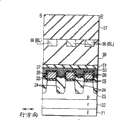
FIG. 3, FIG. 4, FIG. 5, FIG. 6, FIG. 7, FIG. 8, FIG. 9 are cross-sectional views in the directions of arrows A-A ', E-E ' and B-B ', C-C ', D-D ', F-F ', G-G ' of FIG. 2, respectively.
Fig. 3 is a cross-sectional view of a region including a NAND-type memory cell module and a select gate transistor in the a-a' direction. Fig. 4 is a cross-sectional view of the element isolation region in the direction of E-E'. Fig. 5 is a cross-sectional view of a memory cell portion in the direction B-B'. Fig. 6 is a cross-sectional view of the 1 st select gate transistor S1 in the direction C-C 'and fig. 7 in the direction D-D'. Here, fig. 7 is a cross-sectional view of an opening portion of a block insulating film having a slit-like opening, which will be described later. Fig. 8 is a cross-sectional view at the drain electrode in the direction F-F ', and fig. 9 is a cross-sectional view at the source electrode in the direction G-G'.
In FIGS. 2, 3, 5 and 6, for example, the boron impurity concentration is 1014cm-3~1019cm-3On the p- well region 23, 1 st insulating films 25, which are tunnel gate insulating films including, for example, a silicon oxide film or an oxynitride film having a thickness of 3 to 15nm, are formedSSL、25GSL。
In the 1 st insulating films 25, 25SSL、25GSLThe above-mentioned thickness of 10nm to 500nm includes, for example, the addition of 1018cm-3~1021cm-3A floating gate electrode 26 of polysilicon or the like of phosphorus or arsenic, and a 1 st electrode layer 26 which is an electrode layer made of the same electrode material as the floating gate electrode 26SSLAnd the 3 rd electrode layer 26GSL。
These layers are formed on a region where the element isolation insulating film 24 including, for example, a silicon oxide film is not formed, self-aligned with the p-well region 23. That is, after the 1 st insulating film 25 and the floating gate electrode 26 are entirely deposited on the p-well region 23 as a semiconductor region, they are patterned and etched to the p-well region 23, and then the p-well region 23 is etched to a depth of, for example, 0.05 to 0.5 μm. The element isolation insulating film 24 may be buried therein. In this way, since the 1 st insulating film 25 and the floating gate electrode 26 can be formed over the entire surface without steps, deposition with uniform characteristics can be performed with further improved uniformity.
Then, in the present embodiment, when the element isolation insulating film 24 is etched in order to expose the side surface of the floating gate electrode 26, the memory cell column of fig. 2 is not entirely etched, but the range shown in fig. 10 is etched, for example, by using a photoresist and a photolithography process. I.e. the memory cell is partially etched such that it is at least notEtching includes data transmission line contact 31dAnd includes source line contact 31sThe area of (a).
As described above, the module insulating film 50 (No. 2 insulating film) or 50 including, for example, a silicon oxide film or an oxynitride film having a thickness of 5nm to 30nm or a silicon oxide film/silicon nitride film/silicon oxide film is formedSSL(No. 3 insulating film), 50GSL(4 th insulating film).
In addition, the 2 nd, 3 rd and 4 th insulation films 50, 50 are arranged between the twoSSL、50GSLA control gate electrode 27 and a 2 nd electrode layer 27 made of the same electrode material as the control gate electrode 27 are formed in a thickness of 10nm to 500nmSSLAnd a 4 th electrode layer 27GSLWherein control gate electrode 27 comprises a gate electrode of 1017~1021cm-3For example, polysilicon to which impurities such as phosphorus, arsenic, or boron are added, a laminated structure of WSi (tungsten silicide) and polysilicon, or a laminated structure of NiSi, MoSi, TiSi, CoSi, and polysilicon.
The control gate electrode 27 is formed up to a block boundary in the left-right direction on the paper surface of fig. 2 so as to be connected to the memory cell blocks adjacent to each other in fig. 2, and forms data selection lines WL0 to WL 115. Fig. 5 shows a case where the control data electrode 27 is connected to the control gate electrode of the adjacent module via above the element isolation insulating film 24.
Similarly, as shown in FIGS. 6 and 7, the 2 nd electrode layer 27SSLAnd a 4 th electrode layer 27GSLThe 1 st control line SSL and the 2 nd control line GSL are also formed to be connected to the 2 nd electrode layer and the 4 th electrode layer of the adjacent memory cell modules between the element isolation insulating films 24 through the upper sides of the element isolation insulating films 24.
The p-well region 23 may be separated by the n-type silicon region 22 to be applied with a voltage independently of the p-type semiconductor substrate 21. Thus, the circuit load at the time of erasing can be reduced, and power consumption can be suppressed.
In this embodiment, since the side walls of the p-well region 23 are covered with the element isolation insulating film 24, the floating gate electrode 26 can be prevented from falling below the p-well region 23 without being exposed during etching prior to the floating gate electrode 26.
Therefore, a parasitic transistor having a low threshold value and a concentrated gate electric field is less likely to be generated at the boundary between the p-well region 23 and the element isolation insulating film 24. Further, since a phenomenon of a low writing threshold value, which causes electric field concentration, that is, a parasitic channel (sidewalk) phenomenon is less likely to occur, a transistor with higher reliability can be formed.
As shown in fig. 3, sidewall insulating films 43 including, for example, a silicon nitride film or a silicon oxide film having a thickness of 5nm to 200nm are formed on both sides of these gate electrodes. In addition, an n-type diffusion layer 28 to be a source electrode or a drain electrode of each memory cell is formed in the p-well region 23 therebetween.
A floating gate type EEPROM cell having the amount of charge accumulated in the floating gate electrode as the amount of information is formed by the n-type diffusion layer 28, the floating gate electrode 26, and the control gate electrode 27. The gate length is 0.5 μm or less and 0.01 μm or more.
The source-drain n-type diffusion layer 28 is formed so that the surface concentration of, for example, phosphorus or arsenic, antimony is 1017cm-3~1021cm-3The pattern of (1) is formed at a depth of 10nm to 500 nm. These n-type diffusion layers 28 are shared between adjacent memory cells, and implement NAND connections in which current paths of the memory cells are connected in series.
In addition, in FIG. 3, the 1 st electrode layer 26SSLAnd the 3 rd electrode layer 26GSLThe gate electrodes connected to the block selection lines corresponding to the 1 st control line SSL and the 2 nd control line GSL are formed on the same layer as the floating gate electrode 26 of the floating gate EEPROM. Since the 1 st electrode layer 26SSLAnd the 3 rd electrode layer 26GSLThe gate length of (2) is longer than the gate length of the gate electrode of the memory cell, for example, 1 μm or less and 0.02 μm or more, so that it is possible to ensure an increase in the on/off ratio between when the module is selected and when it is not selected, and to prevent erroneous writing or erroneous reading.
In addition, as a current with the 1 st select gate transistor S1N-type diffusion layer 28 of drain electrode connected to one end of via (channel)dThrough data transmission line contacts 31dTo the data transmission line 36 (BL). The data transfer line 36(BL) is formed up to a NAND string boundary in the up-down direction of the paper of fig. 2 to connect to an adjacent NAND string. The data transmission line 36(BL) includes a material such as tungsten, tungsten silicide, titanium, tungsten nitride, or aluminum.
On the other hand, the n-type diffusion layer 28 as a source electrode connected to one end of the current path (channel) of the 2 nd select gate transistor S2sThrough source line contact 31sAnd is connected to a source line 33 (SL). The source line 33(SL) is formed up to a NAND string boundary in the left-right direction of the paper surface in fig. 2 to be connected to an adjacent NAND string. Of course, the n-type diffusion layer (source electrode) 28 may be usedsThe source line is formed up to the NAND string boundary in the left-right direction of the paper.
At these data transmission line contacts 31dAnd source line contact 31sIn the above, the conductive region may be filled with polycrystalline silicon doped with n-type or p-type impurities, tungsten silicide, Al, TiN, Ti, or the like. Between the source line 33 and the data transmission line 36 and the above transistors, a filling material including, for example, SiO is filled2Or an interlayer insulating film 38 of SiN. On the upper portion of the data transmission line 36, a layer including, for example, SiO is formed2An insulating film resist 37 of SiN, polyimide, or the like, and an upper wiring including W, Al, Cu, or the like, for example, which is not shown.
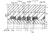
In the 1 st and 2 nd selection gate transistors connected by the selection gate control line SSL (1 st control line) and GSL (2 nd control line), the 3 rd insulating film 50 is formedSSLAnd a 4 th insulating film 50GSLThereafter, as shown by the broken line in fig. 2, adjacent NAND strings between the element isolation regions are etched to commonly form slit-like openings. No. 3 insulating film 50SSLThe slit-shaped opening portions are the 1 st opening portion 11, the 4 th insulating film 50GSLThe slit-like opening portion is a 2 nd opening portion 12.
Thus, in the element region1 electrode layer 26SSLAnd 2 nd electrode layer 27SSLA 1 st gate electrode connected through the 1 st opening portion 11 and formed as a gate electrode of the select gate transistor S1; in addition, the 3 rd electrode layer 26GSLAnd a 4 th electrode layer 27GSLConnected through the 2 nd opening portion 12, and forms a 2 nd gate electrode as a gate electrode of the select gate transistor S2. This is because the off (cut-off) of the select gate transistor S1 and the select gate transistor S2 is good, and the 1 st electrode layer 26 can be prevented from being formedGSLAnd 3 rd electrode layerSSLThe threshold deviation caused by the accumulated charge.
In addition, when the No. 3 insulating film 50 is appliedSSLAnd a 4 th insulating film 50GSLWhen etching is performed so that the opening is slit-shaped, in the element region, the 1 st electrode layer 26 made of the same material as the floating gate electrode 26 under the opening 11 and the opening 12 is formedSSLAnd the 3 rd electrode layer 26GSLAnd carrying out local excavation. Therefore, as shown in FIG. 3, when the 2 nd electrode layer 27 made of the same material as the control gate electrode 27 is formed thereonSSLAnd a 4 th electrode layer 27GSLThen, the first electrode layer 26 passes through the 1 st opening 11 and the 2 nd opening 12 and contacts the 1 st electrode layer 26 in a protruding shape below the openingsSSLAnd the 3 rd electrode layer 26GSLAnd (4) direct connection. By thus making the 2 nd electrode layer 27 separatelySSLIs turned into a direction 26SSLShape of inner protrusion and 4 th electrode layer 27GSLTo the 3 rd electrode layer 26GSLThe shape of the inner protrusion can make the 1 st electrode layer 26SSLAnd the 2 nd electrode layer 27SSLAnd the 3 rd electrode layer 26GSLAnd the 4 th electrode layer 27GSLThe contact area therebetween is increased, and the resistance of the contact portion is reduced.
No. 3 insulating film 50SSLAnd a 4 th insulating film 50GSLAlso in the element isolation region sandwiched by the element regions, and is in direct contact with the upper surface of the element isolation insulating film 24 as shown in fig. 6. As shown by the broken line in fig. 2, the 1 st opening portion 11 and the 2 nd opening portion 12 also have openings in the element isolation region. Therefore, as shown in FIG. 7, the second element widely exists in the element isolation region2 electrode layer 27SSLAnd a 4 th electrode layer 27GSLDirectly contacts the upper surface of the element isolation insulating film 24 through the 1 st opening portion 11 and the 2 nd opening portion 12.
At this time, since the element isolation insulating film 24 under the opening portion 11 and the opening portion 12 is partially dug in etching, in the element isolation region, as shown in FIG. 4, the 2 nd electrode layer 27SSLAnd a 4 th electrode layer 27GSLIn a protruding shape passing through the 1 st opening portion 11 and the 2 nd opening portion 12 and up to the lower side of the opening portions, is in direct contact with the element isolation insulating film 24.
In the present embodiment described above, when the element isolation insulating film 24 is etched, as shown in fig. 10, the data transmission line contact 31 is not etcheddAnd includes source line contact 31sThe area containing the memory cells is etched. At this time, on the element isolation insulating film 24, boundaries between etched regions and unetched regions are represented as boundaries 100, 110, 120 of fig. 2.
In the present embodiment, the etching of the region including the memory cell portion does not reach the 3 rd insulating film 50 as shown by the boundaries 100, 110, and 120SSLAnd a 4 th insulating film 50GSLAnd etching the area into a slit-shaped opening. That is, the 3 rd insulating film 50SSLAnd a 4 th insulating film 50GSLThe region etched into the slit-shaped opening is not repeatedly etched with respect to the element isolation insulating film 24.
Therefore, on the element isolation insulating film 24 forming the element isolation region as shown in fig. 4, the 3 rd insulating film 50 connected to the 1 st and 2 nd selection gate transistor portionsSSLAnd a 4 th insulating film 50GSLAt least at a portion in contact with the opening portionyHeight h of the 2 nd insulating film 50 in contact with the memory cell portionxHigh.
For comparison, when the element isolation insulating film 24 (the entire element isolation is etched back) in the region including the select gate transistor shown in fig. 2, which is different from the present embodiment, is etched back, the cross-sectional views corresponding to fig. 3, 4, 5, 6, 7, 8, and 9 are fig. 11, 12, 13, 14, 15, 16, and 17. Like FIGS. 3 to 9, they are cross-sectional views in the directions of arrows A-A ', E-E ', B-B ', C-C ', D-D ', F-F ', and G-G ' in FIG. 2, respectively.
In contrast to the case of performing the whole surface isolation etch-back in fig. 15, in the present embodiment shown in fig. 7, the 2 nd electrode layer 27 is formed in contact with the element isolation insulating film 24 in the slit-shaped opening portionSSLIs formed at a higher position.
Therefore, to prevent the 2 nd electrode layer 27 in FIG. 15SSLThe 2 nd electrode layer 27 shown in FIG. 7 may be made adjacent to the p-well region 23 of the memory cellSSLAway from the p-well region 23. Therefore, it is similar to the 1 st electrode layer 26 in FIG. 15SSLThe influence on the p-well region 23 of the memory cell when the gate voltage is changed can be reduced as compared with the shape in which the element isolation insulating film 24 protrudes upward.
That is, the first electrode layer 26 is changed in this embodiment mode compared with the case of the whole surface device isolation etch-backSSLThe voltage of (3) can reduce the effect that the electric charge is generated in the p-well region 23 when the electric flux lines reach the upper region of the p-well region 23 from the gate end. Therefore, the problem of the threshold value of the select gate transistor being lowered by the electric charges generated in the p-well region 23 due to the above-described effect can be suppressed.
In programming, for a selected NAND string to which data is not written, first, the gate electrode of the 1 st select-gate transistor S1 is turned on at a high potential to accumulate charges in the NAND string, and then, the potential of the gate electrode is slightly lowered to turn off the NAND string, thereby turning the NAND string into a floating (floating) state. In contrast, if the threshold of the 1 st select gate transistor S1 is too low, it will be a cause of erroneous writing in which the electric charges accumulated in the NAND string 45 leak from the data transfer line 36(BL) side. However, since the embodiment of the present invention can avoid the decrease in the threshold value, it is possible to realize a highly reliable nonvolatile semiconductor device in which the erroneous writing of the cell is suppressed.
The problem with the case of using a global device isolation etchback is that: 2 nd electrode layer 27 on element isolation insulating film 24SSLAnd a 4 th electrode layer 27GSLThe bottom surface height deviation is the etching depth deviation of the whole device isolation etch back and the 3 rd insulating film 50SSLAnd a 4 th insulating film 50GSLThe variation in etching depth when the etching opening is slit-shaped or the total variation in floating gate film thickness increases. This deviation reflects the threshold deviation of the select gate transistor and is one of the main causes of the threshold value being too low.
However, in the present embodiment as described above, since the element isolation insulating film 24 in the region including the memory cell is selectively etched, the slit portion of the select gate transistor and the periphery thereof are not etched as shown in fig. 10. Thus, the 2 nd electrode layer 27 on the element isolation insulating film 24SSLAnd a 4 th electrode layer 27GSLThe bottom surface height deviation of (2) is not added with the etching depth deviation generated by the full surface element isolation back etching. Therefore, the threshold variation of the select gate transistor can be reduced as compared with the case where the entire element isolation etch-back is performed. In this way, it is possible to avoid a large decrease in the threshold value of the select gate transistor, which would otherwise occur when the variation is large, and thus it is possible to obtain an effect of suppressing erroneous writing into the cell.
Since the miniaturization increases the capacitive coupling between adjacent cells and the influence of the depletion layer of the p-well region 23 becomes larger, it is necessary to secure a larger opposing area between the floating gate electrode 26 and the control electrode 27 with the 2 nd insulating film 50 interposed therebetween.
Therefore, if the side surface of the floating gate electrode 26 is largely exposed when the whole surface element isolation etch back is performed, as shown in FIG. 15, the second electrode layer 27 is formed on the second electrode layer 2SSLThe bottom surface in the element isolation region is close to the p-well region 23 of the memory cell, and therefore, there is a problem that the threshold value of the select gate transistor is lowered and the variation thereof becomes large. However, according to the embodiments of the present invention, this problem can be alleviated.
In general, when the threshold value is raised in order to compensate for the variation in the threshold value of the select gate transistor, since the data transfer line 36(BL) cannot supply a sufficiently high voltage to the NAND string 45, the setting margin of the threshold value is limited to a narrow range. However, since the present embodiment can suppress the decrease in the threshold value of the select gate transistor, it is easy to secure the margin. Therefore, it is not necessary to increase the channel concentration in order to increase the threshold of the select gate transistor. Thus, deterioration of junction withstand voltage between the source electrode and the drain electrode and deterioration of junction leakage generated when a voltage of 0V is applied to the gate can be prevented, and leakage of the data transmission line can be prevented.
With the development of microfabrication, a data transmission line contact 31 is formed thereon with respect to the minimum design width F of the celld(BL contact) and source line contact 31sThe length of the p-well region 23 of (SL contact) in the direction parallel to the substrate (the cross-sectional direction of fig. 11) is sufficiently larger than 3F, that is, 3 times.
Therefore, when the element isolation insulating film 24 is subjected to the overall element isolation etch-back, the data transmission line contact 31 is, as shown in fig. 12, due to a micro loading effect of anisotropic etching for gate electrode processingdOne side element isolation region surface 60dOr source line contact 31sOne side element isolation region surface 60sIs dug deeper than the element isolation region surface 60 of the memory cell side. The micro-loading effect is a phenomenon in which, in the case of dry etching, the difference in etching rate is caused by the density of a pattern to be processed.
As a result, as shown in fig. 16 and 17, the height of the upper surface of the element isolation insulating film 24 is lower than the height of the upper surface of the p-well region 23 in the element region.
In contrast, in the present embodiment, as shown in fig. 10, since the element isolation insulating film 24 is not etched back entirely, the data transfer line contact 31 is shown in fig. 4dOne side element isolation region surface 60dAnd source line contact 31sOne-side element isolation regionDomain surface 60sBecomes higher than the element isolation region surface 60 on the memory cell side.
Then, as shown in fig. 8 and 9, the height of the upper surface of the element isolation insulating film 24 in contact with the p-well region 23 for forming the junctions (drain electrode 28d and source electrode 28 s) for the data transfer line contact (BL contact) and the source line contact (SL contact) can be maintained at a higher position than the upper surface of the element region of the p-well region 23 on which the junctions are formed.
That is, the height of the upper surface of the element-separating insulating film 24 in the element-separating region sandwiched between the BL contacts or the SL contacts respectively included in the adjacent NAND strings in fig. 2 is higher than the height of the upper surface of the p-well region 23 in the element region. Here, the upper surface of the element region of the p-well region 23 has a height such that, for example, one end of the current path of the 1 st select gate transistor S1 is in contact with the data transfer line contact 31dThe main surface height of the p-well region 23 as the semiconductor substrate on the element region therebetween, or one end of the current path of the 2 nd select gate transistor S2 and the source line contact 31sThe main surface height of the p-well region 23 as the semiconductor substrate on the element region in between.
Since such an element isolation insulating film 24 is present, formation of the source electrode 28 can be preventedsAnd a drain electrode 28dIs implanted from the side surface of the p-well region 23 of the memory cell which is in contact with the element isolation insulating film 24. Therefore, formation of a deep junction can be prevented.
Since the above-described effect is not obtained in the case where the full-surface element isolation etch-back is performed, the source electrode 28 of the deep junction as shown in fig. 11 is formedsOr drain electrode 28d. As a result, for example, the leakage current of the select gate transistor S2 increases, and the off-state becomes difficult.
However, in the present embodiment as described above, the element isolation region surface 60 as shown in fig. 4d,60sOr as shown in fig. 8 and 9, the upper surface of the element isolation insulating film 24 may be raisedHeight. Therefore, as shown in FIG. 3, the source electrode 28 can be usedsAnd a drain electrode 28dIs formed as a shallow junction so as to avoid the above-mentioned problems. In addition, even to the BL contact 31 on the data transfer line sidedAnd the occurrence of the separation of the drain electrode 28 is also less likelydThe inter-element isolation insulating film 24 is penetrated, and it is possible to prevent a problem that it is difficult to ensure electrical isolation between the data transfer lines (BL).
As described above, in the conventional nonvolatile semiconductor memory device in which the floating gate electrode and the element isolation are formed in self-alignment using the entire-surface element isolation etchback, even in the select gate transistor region, the same material as the floating gate electrode 26 is formed in a protruding shape which greatly protrudes upward from the upper surface of the element isolation insulating film 24.
Therefore, the 3 rd insulating film 50 is reducedSSLAnd a 4 th insulating film 50GSLAn element isolation insulating film 24 etched to the height of the slit-shaped opening portion, a 2 nd electrode layer 27SSLAdjacent to the p-well region 23 of the memory cell. Since the 2 nd electrode layer 27SSLClose to the memory cell p-well region 23 causes the voltage of the floating gate electrode 26 to change and causes the electric flux lines to reach the semiconductor region of the upper half of the p-well region 23 from the gate terminal to generate electric charges in the p-well region 23. Therefore, a problem of lowering the threshold of the select gate transistor is caused.
This causes a problem that charges accumulated in the NAND string selected so that data is not written at the time of programming to accumulate so as not to write data leak from the data transfer line 36 side, which causes a cell erroneous writing.
When the full-surface element isolation etch-back is used, the height of the upper surface of the element isolation insulating film 24, i.e., the 2 nd electrode layer 27SSLAnd a 4 th electrode layer 27GSLIn the element isolation region, except for the film thickness deviation of the floating gate electrode and the 3 rd insulating film 50SSLAnd a 4 th insulating film 50GSLThe etching depth of the slit-shaped opening is not only varied but also varied in addition to the variation in the etching depth of the element isolation insulating film 24. Therefore, the deviation becomes large. As a result thereofResulting in a large reduction of the threshold of the select gate transistor.
When the structure of the nonvolatile semiconductor memory device according to the embodiment of the present invention is used, the slit portion of the select gate transistor and the periphery thereof are not etched as shown in fig. 10 when the element isolation insulating film 24 is etched. Therefore, in the select gate transistor region, the 1 st and 3 rd electrode layers 26 made of the same electrode material as the floating gate electrode 26 can be reduced in sizeSSL、26GSLA protrusion from the upper surface of the element isolation insulating film 24.
That is, as shown in FIG. 7, the 2 nd electrode layer 27 can be preventedSSLAnd a 4 th electrode layer 27GSLThe bottom surface in the element isolation region is close to the p-well region 23 of the memory cell. As a result, a select gate transistor in which the threshold value reduction and the variation thereof are suppressed can be realized.
Therefore, it is possible to prevent the problem that electric charges accumulated for non-writing of data in a NAND string selected so that data is not written at the time of programming leak from the data transfer line side, and it is possible to improve the cell writing characteristics and the read disturb characteristics of the unselected data transfer lines.
In addition, as the micro-fabrication progresses, even if the data transfer line (BL) contact 31 is formeddAnd Source Line (SL) contact 31sThe length of the p-well region 23 is 3 times or more the minimum design width of the cell, and the element isolation insulating film 24 can be formed at a position higher than the upper surface of the p-well region 23 of the memory cell. Therefore, even if the effect of a slight load is caused by anisotropic etching in gate electrode processing, the upper surface of the element isolation insulating film 24 can be kept high
Thus, formation of the source electrode 28 can be preventedsAnd a drain electrode 28dIs implanted from the side of the memory cell p-well region 23 which is in contact with the element isolation region. Thus, directly below the gate, the source electrode 28 of the select gate transistorsAnd a drain electrode 28dDoes not go deeper than the source or drain electrode to be connected to the memory cellThe junction depth of the n-type diffusion layer 28.
Therefore, the source electrode 28 can be prevented from being damagedsAnd a drain electrode 28dIs deeper, which causes a problem that it is difficult to turn off by increasing the leakage of the select gate transistor S2. In addition, the drain electrode 28 at the BL contact on the data transfer line side can be suppresseddCan ensure good electrical isolation between the data transmission lines BL.
Fig. 18 shows a layout plan view of the nonvolatile semiconductor memory device according to embodiment 2 of the present invention. Hereinafter, the same portions as those in fig. 2 are denoted by the same reference numerals, and the description thereof will be omitted. In the drawings, the suffixes of the symbols represent differences in the positions of elements used, and the members having the same main symbol represent the same material formed by the same process.
Fig. 18 shows a structure in which 3 NAND strings shown in the equivalent circuit of fig. 1 are arranged side by side. To facilitate understanding of the cell structure, fig. 18 shows only the structure of the layers below the gate electrode 27. In fig. 18, nonvolatile semiconductor memory cells M0 to M15 each including a MOS transistor having a floating gate electrode 26 are connected in series, and one end is connected to a data transfer line through a selection transistor S1. The other end is connected to the common source line through a select transistor S2.
The nonvolatile semiconductor memory device of the present embodiment shown in fig. 18 is different from that of embodiment 1 shown in fig. 2 in that the 3 rd insulating film 50 is etched in a region larger than the slit-shaped region included in embodiment 1SSLAnd a 4 th insulating film 50GSLAnd (5) removing. That is, in the region on the side of the BL contact and SL contact portions covered by the dotted line in fig. 18, the 3 rd insulating film 50 is etchedSSLAnd a 4 th insulating film 50GSLAnd (5) removing.
Fig. 19 is a cross-sectional view of a region including a NAND-type memory cell module and a select gate transistor in the direction of an arrow a-a' in fig. 18. FIG. 20 is a cross-sectional view of the element isolation region in the direction of the arrow E-E' of FIG. 18
Fig. 21 is a cross-sectional view of a memory cell portion in the direction of arrow B-B' of fig. 18. Fig. 22 is a cross-sectional view of the 1 st select gate transistor S1 in the direction of the arrow C-C 'of fig. 18 and fig. 23 is a cross-sectional view of the arrow D-D' of fig. 18. FIG. 23 is a 3 rd insulating film 50 shown by a dotted line in FIG. 18 and widely openedSSLAnd a 4 th insulating film 50GSLA cross-sectional view of the opening portion of (1).
Fig. 24 is a cross-sectional view at the drain electrode in the direction of the arrow F-F 'of fig. 18, and fig. 25 is a cross-sectional view at the source electrode in the direction of the arrow G-G' of fig. 18.
In this embodiment, as in embodiment 1, when the element isolation insulating film 24 is etched so as to expose the side surface of the floating gate electrode 26, the entire memory cell column in fig. 18 is not etched, but etched in the same range as in fig. 10.
I.e. to at least not etch the data transmission line contacts 31dAnd includes source line contact 31sThe memory cell portion is etched in a manner of the region of (a). At this time, boundaries between the etched region and the unetched region on the element isolation insulating film 24 are shown as boundaries 100, 110, and 120 in fig. 18.
As shown by the boundaries 100, 110, and 120, in this embodiment, the etching of the region including the memory cell portion does not reach the 3 rd insulating film 50 covered by the broken line in fig. 18SSLAnd a 4 th insulating film 50GSLAnd etching and opening the region. Therefore, the No. 3 insulating film 50SSLAnd a 4 th insulating film 50GSLThe region of the etching opening is not repeatedly etched with the etching of the element isolation insulating film 24.
On the element isolation insulating film 24 forming the element isolation region as shown in FIG. 20, a 3 rd insulating film 50 connected to the 1 st select gate transistorSSLAnd a 4 th insulating film 50 connected to the 2 nd select gate transistorGSLAt least at a portion in contact with the opening portionyA height h higher than the 2 nd insulating film 50 in contact with the memory cell portionx。
Since the nonvolatile semiconductor memory device of this embodiment has a structure that can obtain the same effects as those of embodiment 1, a select gate transistor in which the decrease in threshold value and the variation thereof are suppressed can be realized as in embodiment 1.
Therefore, it is possible to prevent the problem that charges accumulated in the selected NAND string at the time of programming, which cause no data to be written, leak from the data transfer line side, and to improve the writing characteristics of the cell and the read disturb characteristics of the unselected data transfer line.
In this embodiment, the 3 rd insulating film 50 in the common region which is on the NAND strings adjacent between the element isolation regions and covered with the broken line in fig. 18 is appliedSSLAnd a 4 th insulating film 50GSLAnd etching the opening. That is, the opening region reaches the edge of the data transfer line contact side or the source line contact side of the select gate transistor.
Since etching can be performed with a larger etching area than in embodiment 1 in which the opening is slit-shaped, a lower resolution and an inexpensive photolithography process than in embodiment 1 can be used. In addition, since it is not necessary to form a fine etching trench, it is also possible to use an inexpensive etching apparatus.
Embodiment 3
Fig. 26 is a layout plan view showing a nonvolatile semiconductor memory device according to embodiment 3 of the present invention. The same portions as those of the nonvolatile semiconductor memory devices of embodiment 1 and embodiment 2 are denoted by the same reference numerals, and descriptions thereof are omitted. In the drawings, the suffixes of the symbols represent differences in the positions of elements used, and the members having the same main symbol represent the same material formed by the same process.
Fig. 26 shows a structure in which 3 NAND strings shown in the equivalent circuit of fig. 1 are arranged side by side. In particular, fig. 26 shows only the structure of the lower layer of the control gate electrode 27 for the sake of easy understanding of the cell structure. In fig. 26, nonvolatile memory cells M0 to M15 each including a MOS transistor having a floating gate electrode 26 are also connected in series, one end of each being connected to a data transfer line via a selection transistor S1, and the other end being connected to a common source line via a selection transistor S2.
Fig. 27 is a cross-sectional view of a region including a NAND-type memory cell module and a select gate transistor in the direction of an arrow a-a' in fig. 26. Fig. 28 is a cross-sectional view of the element isolation region in the direction of the arrow E-E' of fig. 26.
Fig. 29 is a cross-sectional view of a memory cell portion in the direction of arrow B-B' of fig. 26. Fig. 30 is a view in the direction of the arrow C-C 'of fig. 26, and fig. 31 is a view in cross section of the 1 st select gate transistor S1 in the direction of the arrow D-D' of fig. 26. In particular, FIG. 30 shows the data line contact 31 of the 1 st select gate transistor S1dOne side wall insulating film 43dCross-sectional view of (a). FIG. 31 shows a 3 rd insulating film 50 having a slit-shaped opening, which will be described laterSSLAnd a 4 th insulating film 50GSLA cross-sectional view of the opening portion of (1).
Fig. 32 is a cross-sectional view at the drain electrode in the direction of the arrow F-F 'of fig. 26, and fig. 33 is a cross-sectional view at the source electrode in the direction of the arrow G-G' of fig. 26.
In this embodiment, compared to embodiments 1 and 2, the BL contact 31 of the select gate transistor is provided in the present embodimentdAnd SL contact 31sA step is formed on part of one side of the element isolation insulating film 24, for example, a gate side wall insulating film 43 as shown in FIG. 28dThe following is a description. Thus, in fig. 28, the data transmission line contact 31dOne side element isolation region surface 60dAnd source line contact 31sOne side element isolation region surface 60sThe element isolation region surface 60 is higher than the memory cell side.
In this embodiment, as in embodiments 1 and 2, when the element isolation insulating film 24 is etched to expose the side surface of the floating gate electrode 26, the entire memory cell column in fig. 26 is not etched. For example, by using photoresist and a lithographerProcess, as shown by the dotted line boundary of FIG. 26, the area including the memory cell portion is etched without including at least the data transmission line contact 31dAnd source line contact 31sThe region of (a) is etched.
At this time, the actual boundaries between the etched region and the unetched region on the element isolation insulating film 24 are shown by boundaries 260, 262, and 264 in fig. 26. In this embodiment, the boundaries 260, 262, 264 are located closer to the data transmission line contact 31 than in the embodiments 1 and 2dAnd source line contact 31s。
Therefore, etching boundaries 260, 262, 264 at the time of etching the element isolation insulating film 24 are formed on the gate sidewall insulating film 43dThe following is a description. That is, the etching boundaries 260, 262, 264 at the time of etching the element isolation insulating film 24 and the etching of the 3 rd insulating film 50SSLAnd a 4 th insulating film 50GSLWhile the slit-shaped openings formed do not overlap.
In this manner, in the select gate transistor, the 2 nd electrode layer 27 is formedSSLAnd a 4 th electrode layer 27GSLRespectively with the 1 st electrode layer 26SSLAnd the 3 rd electrode layer 26GSLContact with each other, thereby separating the 3 rd insulating film 50SSLAnd a 4 th insulating film 50GSLAnd the distances between the slit-shaped opening portions and the etching boundaries 260, 262, 264.
Therefore, the number of the insulating films 50 interposed therebetween can be reducedSSLAnd a 4 th insulating film 50GSLA 2 nd electrode layer 27 formed on the element isolation insulating film 24SSLAnd a 4 th electrode layer 27GSLDue to the overlap on the slit-shaped opening portions near the etching boundaries 260, 262, 264.
In addition, the etch boundaries 260, 262, 264 do not enter the 1 st electrode layer 26, which is the gate electrode of the select gate transistorSSLAnd the 3 rd electrode layer 26GSLBelow. Therefore, the 1 st electrode layer 26 can be formed on the source and drain electrodes of the select gate transistorSSLAnd the 3 rd electrode layer 26GSLAre equal in height, so that the 1 st electrode layer 26SSLAnd the 3 rd electrode layer 26GSLThe etching uniformity is better.
As in embodiment 1 and embodiment 2, this embodiment can also prevent the source electrode 28s and the drain electrode 28s from being formed in the present embodimentdIs implanted from the side face of the memory cell in contact with the element isolation insulating film 24 of the p-well region 23, thereby preventing formation of a deep junction.
As a result, for example, a problem of difficulty in turning off due to an increase in leakage current through the select gate transistor S2 can be prevented. In addition, even for the data transfer line side BL contact 31dIt is also possible to make it less likely to pass through the drain electrode 28dThe inter-element isolation insulating film 24 is perforated, thereby preventing a problem that it is difficult to maintain electrical isolation between the data transfer lines (BL).
Embodiment 4
Fig. 34 is a plan view showing the layout of the well contact portion of the nonvolatile semiconductor memory device according to embodiment 4 of the present invention. The same portions as those in embodiments 1 to 3 are denoted by the same reference numerals, and detailed description thereof is omitted. In the drawings, the suffixes of the symbols represent differences in the positions of elements used, and the members having the same main symbol represent the same material formed by the same process.
Fig. 35 is a cross-sectional view in the direction of arrow K-K 'of fig. 34, and fig. 36 is a cross-sectional view in the direction of arrow J-J' of fig. 34. Fig. 37 is a sectional view in the direction of the arrow H-H 'of fig. 34, and fig. 38 is a sectional view in the direction of the arrow I-I' of fig. 34.
The present embodiment relates to a well contact portion formed between memory cell string portions of the NAND flash memory in embodiment 3. Fig. 34 shows a p-well contact portion 34 formed in parallel with the NAND strings in the row direction. As will be described later, the well contact 34 is a contact formed to hold the cell p-well region 23 at a fixed potential.
Fig. 39 shows a case where the well contact portion shown in fig. 34 is formed in parallel with the NAND string where the data transfer line (BL) contact of fig. 26 is formed. The semiconductor regions of the strings 342 and 344 and the data transfer line 36 at both ends of fig. 34 are formed in the same manner as the NAND strings, to become dummy cell (dummy cell) regions 342, 344.
As shown in fig. 39, no data transfer line (BL) contact is formed in the dummy cell regions 342 and 344, and the cell p-well contact 34 and the data transfer line (BL) contact 31 can be secureddThe distance between them.
As can be seen from fig. 35, the source/drain n-type regions 28 in the dummy cell regions 342 and 344dAnd p + region 70dIn between, a region where the n-type region of the source/drain is not formed is formed. Accordingly, the source/drain regions 28 of the dummy cell regions 342, 344 are ensureddAnd p + region 70dThe withstand voltage therebetween. In the n-type region 28dAnd p + region 70dIf there is no problem with the breakdown voltage therebetween, an n-type region may be formed here.
As shown in fig. 37, a well contact 34 is formed on the cell p-well 23 via a p + region 70. Further, for example, by connecting the well contact 34 to the wiring layer 35 and connecting the wiring layer 35 to a power supply (not shown), a contact electrode is formed for the cell p-well 23, whereby the potential of the cell p-well 23 can be kept constant.
The diffusion layer forming the p + region 70 is formed, for example, by using boron so that the surface concentration thereof is 1017cm-3~1021cm-3The pattern of (1) is formed at a depth of 10nm to 500 nm. In this embodiment to embodiment 7 described later, a contact having the same pitch as the cell pitch of the data transfer line (BL) contact of the memory cell is shown as the well contact 34. However, if the contact does not protrude below the element isolation insulating film 24, a peripheral contact having a larger diameter, for example, 60nm to 200nm, than the conventional data transmission contact can be applied.
In the related art, as shown in fig. 40, a semiconductor region wider than the width of the semiconductor region of the NAND string is formed, and a p + region is formed on the portion. Fig. 40 is a plan view of well contact portions formed between NAND string portions of a conventional NAND flash memory and arranged in a row direction of NAND strings. Fig. 41 is a cross-sectional view taken along the direction K-K 'of fig. 40, and fig. 42 is a cross-sectional view taken along the direction J-J' of fig. 40.
In particular, fig. 41 shows the cell p-well contacts formed side by side with the NAND strings forming the data transmission line contacts. At both ends of fig. 41 are so-called dummy cell regions 412, 414 which form semiconductor regions and data transfer lines 36 as with NAND strings. Since no data transmission line contact is formed in the dummy cell regions 412 and 414, the cell p-well contact 34 and the data transmission line contact 31 can be maintaineddThe distance between them.
In the related art, when the well contact is formed, as shown in fig. 41, a semiconductor region wider than the width of the semiconductor region of the NAND string is formed, and a p + region 70 is formed on the portiond. Therefore, a photolithography process is required to break the periodicity of the semiconductor region and the element isolation region, thereby forming the p + region 70dIt is extremely difficult that the width of the semiconductor region adjacent to the semiconductor region of (a) is equal to the width of the semiconductor region of the NAND string having the central portion of the cell array with good periodicity.
For example, if p + region 70 is formeddThe width of the semiconductor region adjacent to the semiconductor region of (2) is smaller than the width of the semiconductor region of the NAND string in the central portion of the cell array having good periodicity, and a problem of pattern collapse occurs.
Conversely, for example, if the p + region 70 is formeddHas a width larger than that of the semiconductor region of the NAND string having the central portion of the cell array with good periodicity, and a p + region 70 is formeddThe width of the element isolation insulating film 24 adjacent to the semiconductor region of (a) becomes smaller. Then, the embedding aspect ratio (aspect ratio) of the element isolation insulating film 24 increases, resulting in an adverse effect that the element isolation insulating film 24 cannot be completely embedded in the embedded region.
In both cases, the adjacent control gate electrodes 27 are short-circuited, which causes a reduction in yield and deterioration in reliability.
In this embodiment, as shown in fig. 35, a p + region 70 as a cell p-well contact region is formed in an element region having the same width as the semiconductor region of the NAND string and the same element isolation widthd. Thus, the semiconductor region and the element isolation region having a smaller pitch while ensuring periodicity are realized without requiring a photolithography process for destroying the periodicity of the semiconductor region and the element isolation region.
Therefore, the problem of pattern collapse caused by the conventional method described above and the adverse effect that the embedded region is not completely embedded in the element isolation insulating film 24 can be avoided, and the embedding uniformity of element isolation can be improved, and the yield and reliability can be improved.
As shown in fig. 35, in the nonvolatile semiconductor device according to the embodiment of the present invention, in the semiconductor region 23 where the cell well contact 34 is formed, the height of the element isolation insulating film 24 can be ensured to be higher with respect to the side surface of the cell p-well region 23 as compared with the case of the related art shown in fig. 41.
In this way, since the height of the upper surface of the element isolation insulating film 24 is higher than the upper surface of the cell p-well region 23, it is possible to prevent the p + region 70 from being formed to reduce the contact resistancedIs implanted deeper from the side surface of the cell p-well region 23.
For example, if the p + region 70dWhen the deep formation is made, particularly, the corner portion under the element isolation insulating film 24, stress is easily concentrated at the corner portion, and therefore, a problem arises that a dislocation line is formed near the corner portion in combination with a crystal defect by ion implantation. If the dislocation line penetrates the cell p-well region 23 and the n-type well 22 to reach the p-type substrate 21, leakage and breakdown voltage failure through the dislocation line may occur. However, the p + region 70 of the present embodimentdDoes not reach the corner under the element isolation, the occurrence of this problem can be reduced.
In particular, boron, which is a p-type impurity, has a higher diffusion constant as an impurity in the Si semiconductor than that of the n-type source/drain electrodes, and thus the p + region tends to extend deeper. In contrast, with the structure described in this embodiment, it is possible to prevent the problems of leakage and breakdown voltage failure through the dislocation line. In addition, the shallow p + region 70 can be formeddAnd thus can remain adjacent to the n-type source/drain region 28dA distance between the p + region 70 and the p + regiondAnd n-type source/drain regions 28dAnd a withstand voltage therebetween.
Embodiment 5
Fig. 43 is a plan view showing the layout of the well contact portion of the nonvolatile semiconductor memory device according to embodiment 5 of the present invention. The same portions as those in embodiments 1 to 4 are denoted by the same reference numerals, and detailed description thereof is omitted. In the drawings, the suffixes of the symbols represent differences in the positions of elements used, and the members having the same main symbol represent the same material formed by the same process.
Fig. 44 is a sectional view in the direction of the arrow H-H 'of fig. 43, and fig. 45 is a sectional view in the direction of the arrow I-I' of fig. 43. Since the cross-sectional view in the direction of arrow K-K 'in fig. 43 is the same as that in fig. 35 and the cross-sectional view in the direction of arrow J-J' in fig. 43 is the same as that in fig. 36, the cross-sectional views in the directions of arrow K-K 'and arrow J-J' in fig. 43 are omitted.
The present embodiment relates to a well contact portion formed between memory cell string portions of the NAND flash memory of embodiment 1. Fig. 43 shows the p-well contact portion 34 formed alongside the NAND string in which the data transfer line contact is formed as shown in fig. 2 in the row direction. The well contact portion 34 is a contact formed to hold the cell p-well region 23 at a fixed potential.
As shown in fig. 35, in this embodiment, a p + region 70 as a p-well contact region is also formed in the element region arranged with the same width and the same element isolation width as those of the semiconductor region of the NAND stringd。
In the figure 15Electrode layer 2 27 is shownSSLIn the case of the conventional structure close to the p-well region 23 of the memory cell, threshold lowering occurs even in the select gate transistor close to the p-well contact portion 34 shown in fig. 44. Especially, the 3 rd insulating film 50 is not etchedSSLAnd a 4 th insulating film 50GSLA 2 nd electrode layer 27 as a control gate electrode on the slit-shaped openingSSLAnd a 4 th electrode layer 27GSLEffective gate insulator film to substrate would add insulating film 3 50SSLAnd a 4 th insulating film 50GSLThe amount of (c). Thus, the sub-2 nd electrode layer 27 may occurSSLAnd a 4 th electrode layer 27GSLThe observed transconductance is lower and the turn-off characteristics of the transistor deteriorate.
Therefore, on the dummy cell regions 432 and 434 and the p-well contact portion 34, a problem of leakage of charges selectively accumulated in the NAND string from the data transfer line side is more likely to be caused, and a write stress is applied to the same shape portion (corresponding to the memory cells connected to WL0 to WL 15) as the memory cell of fig. 44. The application of stress during writing and erasing causes an increase in leakage current of the memory cell data select lines WL 0-WL 15.
In contrast, the second electrode layer 27 shown in FIG. 7 is usedSSLThe structure of the present embodiment separated from the p-well region 23 can realize a highly reliable nonvolatile semiconductor memory device in which erroneous writing of cells is suppressed even in the well contact portion 34.
It is needless to say that, in this embodiment, as in embodiment 1, the threshold variation can be reduced while suppressing the decrease in the threshold of the select gate transistor of the memory cell module. Therefore, it is possible to avoid the problem that the electric charges selectively accumulated in the NAND string so that data is not written at the time of programming leak from the data transfer line side, resulting in an effect of suppressing erroneous writing of the memory cell.
Embodiment 6
Fig. 46 is a plan view showing the layout of the well contact portion of the nonvolatile semiconductor memory device according to embodiment 6 of the present invention. The same portions as those in embodiment 5 are denoted by the same reference numerals, and description thereof is omitted. In the drawings, the suffixes of the symbols represent differences in the positions of elements used, and the parts having the same primary symbol represent materials of the same material formed by the same process
Fig. 47 is a cross-sectional view taken along the direction K-K 'of fig. 46, and fig. 48 is a cross-sectional view taken along the direction J-J' of fig. 46. And FIG. 49 is a sectional view taken along the direction H-H 'of FIG. 46, and FIG. 50 is a sectional view taken along the direction I-I' of FIG. 46.
The present embodiment relates to a well contact portion formed between memory cell string portions of the NAND flash memory of embodiment 2. Fig. 46 shows the well contact portions 34 formed side by side in the row direction with the NAND strings forming the data transfer lines shown in fig. 18. The well contact portion 34 is a contact formed to hold the cell p-well region 23 at a fixed potential.
As shown in fig. 47, in this embodiment mode, a p + region 70 serving as a p-well contact region is also formed in an element region arranged with the same width and the same element isolation width as those of the semiconductor region of the NAND stringd。
In addition to the effects obtained by embodiment 5, the following effects can be obtained in this embodiment.
For example, in this embodiment, the pattern surrounded by the broken line in fig. 46 is applied to the 3 rd insulating film 50SSLAnd a 4 th insulating film 50GSLOpening is performed so that etching can be performed over a larger etching area. Thus, an inexpensive photolithography process with lower resolution than those of embodiment 1 and embodiment 5 can be used. Since it is not necessary to form a fine etching trench, an inexpensive etching apparatus can also be used.
Embodiment 7
Fig. 51 and 52 show plan views of the layout of the memory cell column portion and the well contact portion formed side by side therewith, respectively, of the nonvolatile semiconductor memory device according to embodiment 7 of the present invention.
As described below, the same portions as those in embodiments 1 to 6 are denoted by the same reference numerals, and the description thereof is omitted. In the drawings, the suffixes of the symbols represent differences in the positions of elements used, and the members having the same main symbol represent the same material formed by the same process.
Fig. 51 shows a structure in which 3 NAND strings shown in the equivalent circuit of fig. 1 are arranged side by side. Fig. 51 also shows only the structure below the gate electrode 27 for the sake of easy understanding of the cell structure. In fig. 51, nonvolatile memory cells M0 to M15 each including a MOS transistor having a floating gate electrode 26 are connected in series, and one end is connected to a data transfer line through a selection transistor S1. In addition, the other end is connected to the common source line through a selection transistor S2.
Fig. 53 is a sectional view in the direction of the arrow a-a 'of fig. 51, and fig. 54 is a sectional view in the direction of the arrow E-E' of fig. 51. Fig. 53 is a cross-sectional view of a region including a NAND-type memory cell module and a select gate transistor. Fig. 54 is a sectional view of an element isolation region.
Fig. 52 shows the p-well contact portion 34 formed side by side in the row direction with the NAND string shown in fig. 51 where the data transfer line contact is formed. The contact portion 34 is a contact formed to hold the cell p-well region 23 at a fixed potential.
Fig. 55 is a sectional view taken along line H-H 'of fig. 52, and fig. 56 is a sectional view taken along line I-I' of fig. 52. The sectional view in the direction of K-K 'in FIG. 52 is the same as that in FIG. 35, and the sectional view in the direction of J-J' in FIG. 52 is the same as that in FIG. 36, and therefore, it is omitted.
In contrast, in the nonvolatile semiconductor memory device according to embodiment 7 of the present invention, instead of selectively etching the element isolation insulating film 24, when etching control is performedGate electrode 27 and 2 nd electrode layer 27SSLThe 4 th electrode layer 27GSLAn interpoly insulating film 50 (No. 2 insulating film), 50SSL(No. 3 insulating film), 50GSL(4 th insulating film) and floating gate electrode 26, 1 st electrode layer 26SSLThe 3 rd electrode layer 26GSLAt this time, the element-separating insulating film 24 of the memory cell portion is etched without etching the element-separating insulating film 24 of the data transfer line contact and source line contact portions.
In this embodiment mode, the control gate electrode 27 and the 2 nd electrode layer 27 are formed by using a photoresist and a photolithography processSSLThe 4 th electrode layer 27GSL Interpoly insulating films 50, 50SSL、50GSLAnd a floating gate electrode 26 and a 1 st electrode layer 26SSLThe 3 rd electrode layer 26GSLPatterning and anisotropic etching are performed. Accordingly, when the process of exposing the semiconductor substrate of the source and drain electrode portions is performed, the element isolation insulating film 24 of the memory cell portion is etched without etching the element isolation insulating film 24 of the data transfer line contact and the source line contact portion.
In fig. 51 and 52, the line indicating "upper gate boundary" indicates an etching boundary, which may be formed in the upper half of the select gate transistors S1 and S2, but this structure may be combined with the structure of embodiment 1 to 3.
By using the structure of the nonvolatile semiconductor memory device of this embodiment mode, as shown in fig. 54 and 56, the 3 rd insulating film 50 can be formed therebetweenSSLAnd a 4 th insulating film 50GSLA 2 nd electrode layer 27 formed on the element isolation insulating film 24SSLAnd a 4 th electrode layer 27GSLIs fixed.
In general, as microfabrication progresses, the data line contact 31 is formeddAnd source line contact 31sIs sufficiently larger than 3F, i.e., 3 times, the minimum design width F of the cell in the a-a' direction. Therefore, when the element isolation insulating film 24 is subjected to the entire surface element isolation etch-back, the slight negative effect is generated in the anisotropic etching for the gate electrode processingCharge effect, data transmission line contact 31dSide and source line side contacts 31sThe surface of the element isolation region 24 on the side is dug deeper than the surface of the element isolation region 24 on the memory cell side.
In addition, when the gate sidewall insulating film 43 is anisotropically etched, in the case where the gate sidewall insulating film 43 includes a silicon oxide film and the element isolation insulating film 24 includes a silicon oxide film, the element isolation insulating film 24 digs deeper than the gate sidewall insulating film 43 due to the gate sidewall micro-load effect.
In this embodiment, since the gate etching is performed only on the cell portion, the effect of the element isolation insulating film 24 being deeply dug due to the micro-load effect can be alleviated.
In this embodiment, in the semiconductor region 23 where the data line contact and the source line contact are formed as shown in fig. 8 and 9, the height of the upper surface of the element isolation insulating film 24 can be kept higher than the p-well region 23 side than in the related art, and the same effect as in embodiment 1 can be obtained in the memory cell column portion.
As shown in fig. 35, in the semiconductor region 23 where the cell well contact 34 is formed, the present embodiment can keep the height of the element isolation insulating film 24 higher than the side surface of the p-well region 23 of the related art shown in fig. 41.
Therefore, in the same manner as in embodiment 4, when the device is miniaturized, the bottom surface edge portion of the device isolation region can be prevented from interfering with the n-type region formed on the source/drain region or the well contact region+Or a defect caused by overlapping p + regions.
Accordingly, it is possible to prevent the problems of leakage through the dislocation line and breakdown voltage failure, and to improve the reliability of the semiconductor memory device. In addition, p + region 70 can be secureddAnd n-type source/drain regions 28dAnd a withstand voltage therebetween.
In another embodiment of the present invention, the silicon nitride film may be formed as an element isolation insulating film or an insulating film for converting silicon into a silicon oxide film or a silicon nitride filmForming; further, a method of implanting oxygen ions into the deposited silicon, or a method of oxidizing the deposited silicon, for example, may also be used. In addition, TiO may be used as the insulating film2Or Al2O3HFAlO, HFSiO, a tantalum oxide film, strontium titanate or barium titanate, lead zirconium titanate, or a laminated film thereof.
In the above embodiments, a p-type Si substrate is used as the semiconductor substrate, but an n-type Si substrate or an SOI substrate may be used, or another single crystal semiconductor substrate containing silicon such as a SiGe mixed crystal or a SiGeC mixed crystal may be used.
In addition, the control gate electrode 27 and the 2 nd electrode layer 27SSLThe 4 th electrode layer 27GSLAlternatively, a silicide or polycide such as SiGe mixed crystal, SiGeC mixed crystal, TiSi, NiSi, CoSi, TaSi, WSi, MoSi, or a metal such as Ti, Al, Cu, TiN, or W may be used, or a polycrystalline material or a layered structure thereof may be used.
In addition, the floating gate electrode 26 and the 1 st electrode layer 26SSLAnd the 3 rd electrode layer 26GSLAmorphous silicon, amorphous SiGe, amorphous SiGeC, or a laminated structure thereof may also be used.
An aspect of the present invention is to provide a nonvolatile semiconductor memory device that improves memory cell writing characteristics by preventing a threshold value of a select gate transistor from being lowered.
Other modifications and variations to the above-described invention may be readily apparent to those skilled in the art. Therefore, the invention is not limited to the specific details and representative embodiments described in this application. Therefore, various modifications can be made without departing from the spirit and scope of the present invention defined by the claims and the like of the present application.
Claims (20)
1. A non-volatile semiconductor memory device comprising a plurality of NAND strings arranged side by side, each of said NAND strings comprising:
a memory cell module in which current paths of a plurality of nonvolatile memory cells are connected in series, each memory cell including a floating gate electrode formed on an element region separated by an element isolation insulating film forming an element isolation region on a semiconductor substrate with a 1 st insulating film interposed therebetween, and a control gate electrode formed on the floating gate electrode with a 2 nd insulating film interposed therebetween so as to cover side surfaces and an upper surface of the floating gate electrode;
a 1 st select gate transistor having a 1 st electrode layer of the same electrode material as the floating gate electrode and a 2 nd electrode layer of the same electrode material as the control gate electrode, a 1 st gate electrode formed by direct connection through a 1 st opening formed in a part of a 3 rd insulating film of the same insulating material as the 2 nd insulating film, one end of a current path thereof being connected to one end of a current path of the nonvolatile memory cells connected in series in the memory cell module, and the other end of the current path thereof being connected to a data transmission line through a data transmission line contact; and
a 2 nd selective gate transistor having a 3 rd electrode layer of the same electrode material as the floating gate electrode, a 4 th electrode layer of the same electrode material as the control gate electrode, and a 2 nd gate electrode formed by direct connection through a 2 nd opening formed in a part of a 4 th insulating film of the same insulating material as the 2 nd insulating film, one end of a current path of the 2 nd selective gate transistor being connected to the other end of a current path of the nonvolatile memory cells connected in series in the memory cell module, and the other end of the current path being connected to a source line through a source line contact;
wherein the height of the upper surface of the element isolation insulating film between the data line contacts on the adjacent NAND strings is higher than the height of the main surface of the semiconductor substrate in an element region between the other end of the current path of the 1 st select gate transistor and the data line contact; or,
the height of the upper surface of the element isolation insulating film between the source line contacts included in the adjacent NAND strings is higher than the height of the main surface of the semiconductor substrate in an element region between the other end of the current path of the 2 nd select gate transistor and the source line contact.
2. The nonvolatile semiconductor memory device according to claim 1,
the 2 nd electrode layer is formed to be in direct contact with the 1 st electrode layer at a position lower than the height of the bottom surface of the 3 rd insulating film including the inside of the 1 st opening in the element region,
the 4 th electrode layer is formed to a position lower than the height of the bottom surface of the 4 th insulating film including the inside of the 2 nd opening in the element region, and is in direct contact with the 3 rd electrode layer.
3. The nonvolatile semiconductor memory device according to claim 2,
the 2 nd electrode layer is formed to a position lower than the bottom surface of the 3 rd insulating film including the inside of the 1 st opening in the element isolation region so as to be in direct contact with the element isolation insulating film, or
The 4 th electrode layer is formed to a position lower than the height of the bottom surface of the 4 th insulating film including the inside of the 2 nd opening in the element isolation region, and is in direct contact with the element isolation insulating film.
4. The nonvolatile semiconductor memory device according to claim 1, further comprising a well contact for holding a potential of a semiconductor region under said 1 st insulating film constant, wherein,
the well contact is formed in another element region having the same width as the element region, which is arranged side by side with the NAND string, with another element isolation region having the same width as the element region interposed therebetween.
5. The nonvolatile semiconductor memory device according to claim 1,
also comprises the following steps of (1) preparing,
a plurality of data selection lines orthogonal to the data transmission lines, connecting control gate electrodes of nonvolatile memory cells of the plurality of memory cell modules separated by the element isolation region, and being parallel to each other;
a 1 st control line parallel to the plurality of data selection lines and connecting 1 st gate electrodes of the plurality of 1 st selection gate transistors separated by the element isolation region; and
a 2 nd control line parallel to the data selection lines and connecting 2 nd gate electrodes of the 2 nd selection gate transistors separated by the element isolation region,
wherein a plurality of the data transmission lines are formed in parallel with each other, and one data transmission line is provided for each of the NAND strings.
6. The nonvolatile semiconductor memory device according to claim 1, further comprising, on said semiconductor substrate, a conductive well,
wherein the memory cell module and the 1 st and 2 nd select gate transistors are formed in the conductive well.
7. A nonvolatile semiconductor memory device comprising:
a memory cell module in which current paths of a plurality of nonvolatile memory cells are connected in series, each memory cell including a floating gate electrode formed on an element region separated by an element isolation insulating film forming an element isolation region on a semiconductor substrate with a 1 st insulating film interposed therebetween, and a control gate electrode formed on the floating gate electrode with a 2 nd insulating film interposed therebetween so as to cover side surfaces and an upper surface of the floating gate electrode;
a 1 st select gate transistor having a 1 st electrode layer of the same electrode material as the floating gate electrode and a 2 nd electrode layer of the same electrode material as the control gate electrode, a 1 st gate electrode formed by direct connection through a 1 st opening formed in a part of a 3 rd insulating film of the same insulating material as the 2 nd insulating film, one end of a current path thereof being connected to one end of a current path of the nonvolatile memory cells connected in series in the memory cell module, and the other end of the current path thereof being connected to a data transmission line through a data transmission line contact; and
a 2 nd select gate transistor having a 3 rd electrode layer of the same electrode material as the floating gate electrode and a 4 th electrode layer of the same electrode material as the control gate electrode, a 2 nd gate electrode formed by direct connection through a 2 nd opening portion formed in a part of a 4 th insulating film of the same insulating material as the 2 nd insulating film, one end of a current path thereof being connected to the other end of the current path of the nonvolatile memory cells connected in series in the memory cell module, and the other end of the current path thereof being connected to a source line through a source line contact;
wherein the height of the bottom surface of the 3 rd insulating film formed in the element isolation region in contact with the 1 st opening portion is higher than the height of the bottom surface of the 2 nd insulating film formed in the element isolation region; or,
the height of the bottom surface of the 4 th insulating film formed in the element isolation region in contact with the 2 nd opening portion is higher than the height of the bottom surface of the 2 nd insulating film formed in the element isolation region.
8. The nonvolatile semiconductor memory device according to claim 7,
the 2 nd electrode layer is formed to be in direct contact with the 1 st electrode layer at a position lower than the height of the bottom surface of the 3 rd insulating film including the inside of the 1 st opening in the element region,
the 4 th electrode layer is formed to a position lower than the height of the bottom surface of the 4 th insulating film including the inside of the 2 nd opening in the element region, and is in direct contact with the 3 rd electrode layer.
9. The nonvolatile semiconductor memory device according to claim 8,
the 2 nd electrode layer is formed to a position lower than the bottom surface of the 3 rd insulating film including the inside of the 1 st opening in the element isolation region so as to be in direct contact with the element isolation insulating film, or
The 4 th electrode layer is formed to a position lower than the height of the bottom surface of the 4 th insulating film including the inside of the 2 nd opening in the element isolation region, and is in direct contact with the element isolation insulating film.
10. The nonvolatile semiconductor memory device according to claim 7,
also comprises the following steps of (1) preparing,
a plurality of data selection lines orthogonal to the data transmission lines, connecting control gate electrodes of nonvolatile memory cells of the plurality of memory cell modules separated by the element isolation region, and being parallel to each other;
a 1 st control line parallel to the plurality of data selection lines and connecting 1 st gate electrodes of the plurality of 1 st selection gate transistors separated by the element isolation region; and
a 2 nd control line parallel to the data selection lines and connecting 2 nd gate electrodes of the 2 nd selection transistors separated by the element isolation region,
wherein a plurality of the memory cell modules are formed so as to be arranged side by side with the element isolation region interposed therebetween; a plurality of data transmission lines are formed in parallel with each other, and each of the memory cell modules has one of the data transmission lines.
11. The nonvolatile semiconductor memory device according to claim 7, further comprising, on said semiconductor substrate, a conductive well,
wherein the memory cell module and the 1 st and 2 nd select gate transistors are formed in the conductive well.
12. A nonvolatile semiconductor memory device comprising a plurality of NAND strings arranged side by side, each of the NAND strings comprising:
a memory cell module in which current paths of a plurality of nonvolatile memory cells are connected in series, each memory cell including a floating gate electrode formed on an element region separated by an element isolation insulating film forming an element isolation region on a semiconductor substrate with a 1 st insulating film interposed therebetween, and a control gate electrode formed on the floating gate electrode with a 2 nd insulating film interposed therebetween so as to cover side surfaces and an upper surface of the floating gate electrode;
a 1 st select gate transistor having a 1 st electrode layer of the same electrode material as the floating gate electrode and a 2 nd electrode layer of the same electrode material as the control gate electrode, a 1 st gate electrode formed by direct connection through a 1 st opening formed in a part of a 3 rd insulating film of the same insulating material as the 2 nd insulating film, one end of a current path thereof being connected to one end of a current path of the nonvolatile memory cells connected in series in the memory cell module, and the other end of the current path thereof being connected to a data transmission line through a data transmission line contact; and
a 2 nd select gate transistor having a 3 rd electrode layer of the same electrode material as the floating gate electrode and a 4 th electrode layer of the same electrode material as the control gate electrode, a 2 nd gate electrode formed by direct connection through a 2 nd opening portion formed in a part of a 4 th insulating film of the same insulating material as the 2 nd insulating film, one end of a current path thereof being connected to the other end of the current path of the nonvolatile memory cells connected in series in the memory cell module, and the other end of the current path thereof being connected to a source line through a source line contact;
wherein the height of the upper surface of the element isolation insulating film between the data transfer line contacts respectively included in the adjacent NAND strings is higher than the height of the upper surface of the element isolation insulating film in a region sandwiched by the same electrode material as the control gate electrode, which connects the control gate electrodes respectively included in the adjacent NAND strings; or,
the height of the upper surface of the element isolation insulating film between the source line contacts included in the adjacent NAND strings is higher than the height of the upper surface of the element isolation insulating film in a region sandwiched by the same electrode material as the control gate electrode, which connects the control gate electrodes included in the adjacent NAND strings.
13. The nonvolatile semiconductor memory device according to claim 12,
the 2 nd electrode layer is formed to be in direct contact with the 1 st electrode layer at a position lower than the height of the bottom surface of the 3 rd insulating film including the inside of the 1 st opening in the element region,
the 4 th electrode layer is formed to a position lower than the height of the bottom surface of the 4 th insulating film including the inside of the 2 nd opening in the element region, and is in direct contact with the 3 rd electrode layer.
14. The nonvolatile semiconductor memory device according to claim 13,
the 2 nd electrode layer is formed to a position lower than the bottom surface of the 3 rd insulating film including the inside of the 1 st opening in the element isolation region so as to be in direct contact with the element isolation insulating film, or
The 4 th electrode layer is formed to a position lower than the height of the bottom surface of the 4 th insulating film including the inside of the 2 nd opening in the element isolation region, and is in direct contact with the element isolation insulating film.
15. The nonvolatile semiconductor memory device according to claim 12, further comprising a well contact for holding a potential of the semiconductor region under said 1 st insulating film constant, wherein,
the well contact is formed in another element region having the same width as the element region, which is arranged side by side with the NAND string, with another element isolation region having the same width as the element region interposed therebetween.
16. The nonvolatile semiconductor memory device according to claim 12,
also comprises the following steps of (1) preparing,
a plurality of data selection lines orthogonal to the data transmission lines, connecting control gate electrodes of nonvolatile memory cells of the plurality of memory cell modules separated by the element isolation region, and being parallel to each other;
a 1 st control line parallel to the plurality of data selection lines and connecting 1 st gate electrodes of the plurality of 1 st selection gate transistors separated by the element isolation region; and
a 2 nd control line parallel to the data selection lines and connecting 2 nd gate electrodes of the 2 nd selection gate transistors separated by the element isolation region,
wherein a plurality of the data transmission lines are formed in parallel with each other, and one data transmission line is provided for each of the NAND strings.
17. A nonvolatile semiconductor memory device including a plurality of NAND strings arranged side by side, each of the NAND strings comprising:
a memory cell module in which current paths of a plurality of nonvolatile memory cells are connected in series, each memory cell including a floating gate electrode formed on an element region separated by an element isolation insulating film forming an element isolation region on a semiconductor substrate with a 1 st insulating film interposed therebetween, and a control gate electrode formed on the floating gate electrode with a 2 nd insulating film interposed therebetween so as to cover side surfaces and an upper surface of the floating gate electrode;
a 1 st select gate transistor having a 1 st gate electrode, one end of a current path of which is connected to one end of a current path of nonvolatile memory cells connected in series in the memory cell module, and the other end of the current path of which is connected to a data transfer line through a data transfer line contact, the 1 st gate electrode being formed in such a manner that at least a part of an upper surface of a 1 st electrode layer of the same electrode material as the floating gate electrode is covered with a 3 rd insulating film of the same insulating material as the 2 nd insulating film, and a 2 nd electrode layer of the same electrode material as the control gate electrode covers the upper surface of the 3 rd insulating film and is in direct contact with the 1 st electrode layer; and
a 2 nd selection gate transistor having a 2 nd gate electrode, one end of a current path of which is connected to the other end of the current path of the nonvolatile memory cells connected in series in the memory cell module, and the other end of the current path of which is connected to a source line through a source line contact, the 2 nd gate electrode being formed in such a manner that at least a part of an upper surface of a 3 rd electrode layer of the same electrode material as the floating gate electrode is covered with a 4 th insulating film of the same insulating material as the 2 nd insulating film, and a 4 th electrode layer of the same electrode material as the control gate electrode covers the upper surface of the 4 th insulating film and is in direct contact with the 3 rd electrode layer;
wherein the height of the upper surface of the element isolation insulating film between the data transfer line contacts in the adjacent NAND strings is higher than the height of the main surface of the semiconductor substrate in an element region between the other end of the current path of the 1 st select gate transistor and the data transfer line contact; or,
the height of the upper surface of the element isolation insulating film between the source line contacts included in the adjacent NAND strings is higher than the height of the main surface of the semiconductor substrate in an element region between the other end of the current path of the 2 nd select gate transistor and the source line contact.
18. The nonvolatile semiconductor memory device according to claim 17,
the 2 nd electrode layer is formed to a position lower than the height of the bottom surface of the 3 rd insulating film in the element region so as to be in direct contact with the 1 st electrode layer,
the 4 th electrode layer is formed to a position lower than the bottom surface of the 4 th insulating film in the element region, and is in direct contact with the 3 rd electrode layer.
19. The nonvolatile semiconductor memory device according to claim 17, further comprising a well contact for holding a potential of the semiconductor region under said 1 st insulating film constant, wherein,
the well contact is formed in another element region having the same width as the element region, which is arranged side by side with the NAND string, with another element isolation region having the same width as the element region interposed therebetween.
20. The nonvolatile semiconductor memory device according to claim 17,
also comprises the following steps of (1) preparing,
a plurality of data selection lines orthogonal to the data transmission lines, connecting control gate electrodes of nonvolatile memory cells of the plurality of memory cell modules separated by the element isolation region, and being parallel to each other;
a 1 st control line parallel to the plurality of data selection lines and connecting 1 st gate electrodes of the plurality of 1 st selection gate transistors separated by the element isolation region; and
a 2 nd control line parallel to the data selection lines and connecting 2 nd gate electrodes of the 2 nd selection gate transistors separated by the element isolation region,
wherein a plurality of the data transmission lines are formed in parallel with each other, and one data transmission line is provided for each of the NAND strings.
Applications Claiming Priority (3)
| Application Number | Priority Date | Filing Date | Title |
|---|---|---|---|
| JP2006013761 | 2006-01-23 | ||
| JP2006013761 | 2006-01-23 | ||
| JP2006140327 | 2006-05-19 |
Publications (2)
| Publication Number | Publication Date |
|---|---|
| CN101009290A CN101009290A (en) | 2007-08-01 |
| CN100517723C true CN100517723C (en) | 2009-07-22 |
Family
ID=38697581
Family Applications (1)
| Application Number | Title | Priority Date | Filing Date |
|---|---|---|---|
| CNB2007100044461A Expired - Fee Related CN100517723C (en) | 2006-01-23 | 2007-01-23 | Nonvolatile semiconductor storage device |
Country Status (1)
| Country | Link |
|---|---|
| CN (1) | CN100517723C (en) |
Families Citing this family (6)
| Publication number | Priority date | Publication date | Assignee | Title |
|---|---|---|---|---|
| US8441850B2 (en) * | 2010-10-08 | 2013-05-14 | Qualcomm Incorporated | Magnetic random access memory (MRAM) layout with uniform pattern |
| US8946808B2 (en) * | 2012-02-09 | 2015-02-03 | SK Hynix Inc. | Semiconductor device and method of manufacturing the same |
| CN104659203B (en) * | 2013-11-21 | 2018-01-05 | 华邦电子股份有限公司 | Resistive memory element and operation method thereof |
| US10825914B2 (en) * | 2017-11-13 | 2020-11-03 | Taiwan Semiconductor Manufacturing Company, Ltd. | Manufacturing method of semiconductor device |
| TWI816359B (en) * | 2019-03-15 | 2023-09-21 | 日商鎧俠股份有限公司 | Semiconductor device |
| JP2020155755A (en) * | 2019-03-15 | 2020-09-24 | キオクシア株式会社 | Semiconductor device |
Citations (2)
| Publication number | Priority date | Publication date | Assignee | Title |
|---|---|---|---|---|
| CN1591677A (en) * | 2003-08-29 | 2005-03-09 | 株式会社东芝 | Non-volatile semiconductor storage device and its mfg method |
| CN1591904A (en) * | 2003-09-05 | 2005-03-09 | 株式会社瑞萨科技 | Semiconductor device and manufacturing method thereof |
-
2007
- 2007-01-23 CN CNB2007100044461A patent/CN100517723C/en not_active Expired - Fee Related
Patent Citations (2)
| Publication number | Priority date | Publication date | Assignee | Title |
|---|---|---|---|---|
| CN1591677A (en) * | 2003-08-29 | 2005-03-09 | 株式会社东芝 | Non-volatile semiconductor storage device and its mfg method |
| CN1591904A (en) * | 2003-09-05 | 2005-03-09 | 株式会社瑞萨科技 | Semiconductor device and manufacturing method thereof |
Also Published As
| Publication number | Publication date |
|---|---|
| CN101009290A (en) | 2007-08-01 |
Similar Documents
| Publication | Publication Date | Title |
|---|---|---|
| KR100801391B1 (en) | Nonvolatile semiconductor memory | |
| JP4102112B2 (en) | Semiconductor device and manufacturing method thereof | |
| US20100155813A1 (en) | Semiconductor memory device having stack gate structure and method for manufacturing the same | |
| TWI491029B (en) | Scalable gate logic non-volatile memory cells and arrays | |
| US8604517B2 (en) | Non-volatile semiconductor memory device for suppressing deterioration in junction breakdown voltage and surface breakdown voltage of transistor | |
| US8212303B2 (en) | Nonvolatile semiconductor memory device | |
| CN104752435A (en) | Semiconductor device | |
| CN101656257A (en) | Semiconductor memory device | |
| US20080006885A1 (en) | Semiconductor integrated circuit device and method of manufacturing | |
| US8134201B2 (en) | Semiconductor memory device provided with stacked layer gate including charge accumulation layer and control gate, and manufacturing method thereof | |
| CN100517723C (en) | Nonvolatile semiconductor storage device | |
| JP4504403B2 (en) | Semiconductor memory device | |
| US8258569B2 (en) | Non-volatile semiconductor memory device | |
| JP2008098313A (en) | Semiconductor memory device | |
| US7772618B2 (en) | Semiconductor storage device comprising MIS transistor including charge storage layer | |
| US20100001401A1 (en) | Semiconductor device including interconnect layer made of copper | |
| US7439133B2 (en) | Memory structure and method of manufacturing a memory array | |
| JP2010212506A (en) | Semiconductor memory device and method of manufacturing the same | |
| JP2007201244A (en) | Semiconductor device | |
| JP2008166415A (en) | Semiconductor device and manufacturing method thereof | |
| CN111916456B (en) | Scalable logic gate non-volatile memory array and method of manufacturing the same | |
| JP4047500B2 (en) | Semiconductor device and manufacturing method thereof | |
| JP4480541B2 (en) | Nonvolatile semiconductor memory device | |
| JP2010040539A (en) | Method for manufacturing nonvolatile semiconductor memory device, and nonvolatile semiconductor memory device | |
| JP2010103359A (en) | Semiconductor device and method of manufacturing the same |
Legal Events
| Date | Code | Title | Description |
|---|---|---|---|
| C06 | Publication | ||
| PB01 | Publication | ||
| C10 | Entry into substantive examination | ||
| SE01 | Entry into force of request for substantive examination | ||
| C14 | Grant of patent or utility model | ||
| GR01 | Patent grant | ||
| C17 | Cessation of patent right | ||
| CF01 | Termination of patent right due to non-payment of annual fee |
Granted publication date: 20090722 Termination date: 20140123 |