CN100509994C - Light emitting film, luminescent device, method for manufacturing light emitting film and method for manufacturing luminescent device - Google Patents
Light emitting film, luminescent device, method for manufacturing light emitting film and method for manufacturing luminescent device Download PDFInfo
- Publication number
- CN100509994C CN100509994C CNB200480006816XA CN200480006816A CN100509994C CN 100509994 C CN100509994 C CN 100509994C CN B200480006816X A CNB200480006816X A CN B200480006816XA CN 200480006816 A CN200480006816 A CN 200480006816A CN 100509994 C CN100509994 C CN 100509994C
- Authority
- CN
- China
- Prior art keywords
- light
- phosphor
- emitting device
- resin
- emitting element
- Prior art date
- Legal status (The legal status is an assumption and is not a legal conclusion. Google has not performed a legal analysis and makes no representation as to the accuracy of the status listed.)
- Expired - Fee Related
Links
Images


Classifications
-
- H10W72/0198—
-
- H10W72/01515—
-
- H10W72/07251—
-
- H10W72/075—
-
- H10W72/07554—
-
- H10W72/20—
-
- H10W72/536—
-
- H10W72/5363—
-
- H10W72/547—
-
- H10W72/884—
-
- H10W74/00—
-
- H10W90/722—
-
- H10W90/756—
Landscapes
- Luminescent Compositions (AREA)
Abstract
Description
技术领域 technical field
本发明涉及可以用于照明用光源、LED显示器、背光光源、信号机、照明式开关、各种传感器以及各种指示器等方面的发光膜、发光装置以及这些发光膜、发光装置的制造方法。The present invention relates to a luminescent film, a luminescent device, and a method for manufacturing the luminescent film and luminescent device, which can be used in light sources for illumination, LED displays, backlight sources, signal machines, illuminated switches, various sensors, and various indicators.
背景技术 Background technique
人们已经开发出了这样一种发光装置,该装置借助于荧光体对发光元件的光的一部分进行波长转换,并将进行过波长转换的光和未进行过波长转换的发光元件的光混合后使之发射出来,藉此发出发光颜色与发光元件的光不同的光(例如特开2002-198573号公报)。例如,一种白色LED发光装置已经实用化,该装置将使用InGaN系材料的蓝色发光二极管(以下也称为“LED”)用作发光元件,并在发光元件表面涂覆有荧光构件,所述荧光构件由含有可以用组成式(Y、Gd)3(Al、Ga)5O12表示的钇铝石榴石(以下也称为“YAG”)系荧光体的环氧树脂等透光性材料构成。白色LED发光装置的发光颜色可以通过光的混合原理而得到。从LED发射出来的蓝色发光入射到荧光构件之中以后,在层内反复进行吸收和散射,然后向外发射出来。另一方面,被荧光体吸收的蓝色光作为激发源产生作用,发出黄色的荧光。使该荧光体的黄色光和LED的蓝色光混合,人的眼睛便可以看到白光。People have developed such a light-emitting device, which converts a part of the light of the light-emitting element by means of a phosphor, and mixes the wavelength-converted light and the light of the light-emitting element that has not undergone wavelength conversion. It is emitted, thereby emitting light with a color different from that of the light-emitting element (for example, Japanese Patent Application Laid-Open No. 2002-198573). For example, a white LED light-emitting device has been put into practical use. This device uses a blue light-emitting diode (hereinafter also referred to as "LED") using an InGaN-based material as a light-emitting element, and a fluorescent member is coated on the surface of the light-emitting element. The fluorescent member is made of a translucent material such as epoxy resin containing yttrium aluminum garnet (hereinafter also referred to as "YAG")-based phosphor that can be represented by the composition formula (Y, Gd) 3 (Al, Ga) 5 O 12 constitute. The luminous color of the white LED light emitting device can be obtained through the principle of light mixing. After the blue light emitted from the LED enters the fluorescent member, it is repeatedly absorbed and scattered in the layer, and then emitted outward. On the other hand, the blue light absorbed by the phosphor acts as an excitation source to emit yellow fluorescence. By mixing the yellow light of the phosphor with the blue light of the LED, the human eye can see white light.
使用这样的LED的LED发光装置,其特点是小型、电力效率高以及发出颜色鲜艳的光。另外,LED因为是半导体元件,所以不用担心产生烧坏(burn out)等现象。再者,LED发光装置还具有初期激励特性优良、振动和通-断点灯的反复能力较强这样的特征。因为具有这样优良的特征,所以LED发光装置可以作为各种光源加以利用。An LED light-emitting device using such an LED is characterized in that it is compact, has high power efficiency, and emits brightly colored light. In addition, because the LED is a semiconductor element, there is no need to worry about burning out (burn out). Furthermore, the LED light-emitting device also has the characteristics of excellent initial excitation characteristics, strong vibration and repeatability of on-off lighting. Because of such excellent characteristics, LED lighting devices can be utilized as various light sources.
但是,以前的白色发光装置因为大量使用树脂,所以当用于输出功率高、波长短的发光元件时,存在树脂发生退化的问题。另外,在使用无机系粘结剂的情况下,特别在使用由二氧化硅凝胶形成的固化膜的情况下,当曝露在高输出功率和紫外线的环境中时,存在着色退化并产生黑化的问题。虽然其原因尚不清楚,但一般认为这是因为二氧化硅溶胶中所含的有机基团在固化后仍有残留,这些有机基团因强烈的光激发作用而被还原。However, conventional white light-emitting devices use a large amount of resin, so when used in a light-emitting element with high output power and short wavelength, there is a problem that the resin degrades. In addition, in the case of using an inorganic binder, especially in the case of using a cured film formed of silica gel, when exposed to an environment of high output power and ultraviolet rays, there is coloring degradation and blackening The problem. Although the reason for this is unclear, it is generally considered that the organic groups contained in the silica sol remain after curing, and these organic groups are reduced by strong photoexcitation.
另外,为了改善发光装置的光取出效率,可以考虑提高发光膜的透过率。发光膜的透过率依赖于在发光膜中附载荧光体的粘结剂的透过率。当使用在粘结剂中使溶胶热固化而形成的凝胶时,如图1所示,一般可以认为随着溶胶-凝胶反应的进行,越是接近多晶体,发光膜的透过率像图中A所示的那样就越上升。In addition, in order to improve the light extraction efficiency of the light-emitting device, it is conceivable to increase the transmittance of the light-emitting film. The transmittance of the luminescent film depends on the transmittance of the binder carrying the phosphor on the luminescent film. When using a gel formed by thermally curing the sol in a binder, as shown in Figure 1, it can generally be considered that as the sol-gel reaction proceeds, the closer it is to polycrystalline, the transmittance of the luminescent film is like As shown in A in the figure, it rises further.
但是,如果使凝胶接近多晶体,则溶胶-凝胶反应成为在高温下进行的反应,因而需要更多的时间和能量。再者,因为高温,所以存在对半导体发光元件和荧光体产生不良影响的问题。例如连接LED芯片的引线因热而破损,或者荧光体产生退化。为了提高光的取出效率,随着溶胶-凝胶反应的进行而产生多晶体的无机玻璃化,这从反应温度方面来看,伴随着困难的发生。However, if the gel is made close to polycrystalline, the sol-gel reaction will be a reaction at high temperature, requiring more time and energy. Furthermore, due to the high temperature, there is a problem of adverse effects on semiconductor light emitting elements and phosphors. For example, lead wires connecting LED chips are damaged due to heat, or phosphors are degraded. In order to improve the light extraction efficiency, inorganic vitrification of polycrystals occurs as the sol-gel reaction progresses, which is accompanied by difficulties in terms of reaction temperature.
再者,即使随着溶胶-凝胶反应的进行而产生无机玻璃化,发光膜与发光元件的界面也会产生各种问题。例如在玻璃化的界面产生全反射,导致光的取出效率低下,或者产生如下的问题,即发生固化而在发光元件的界面与荧光体的界面形成空间层,空间层成为阻挡层而使光的取出变得困难。Furthermore, even if inorganic vitrification occurs as the sol-gel reaction progresses, various problems arise at the interface between the light-emitting film and the light-emitting element. For example, total reflection occurs at the vitrified interface, resulting in low light extraction efficiency, or the following problems occur, that is, curing occurs to form a space layer at the interface of the light emitting element and the interface of the phosphor, and the space layer becomes a blocking layer to prevent light from being released. It becomes difficult to take out.
另外,在使用LED等发光元件激发发光层的结构中,也存在发光层因曝露在LED的激发光的强大能量中而产生退化的问题。退化的发光层着色为带有黑色,因而有损于本来的透光性,导致光的取出效率恶化。这样黑化的着色退化的原因尚不清楚,但一般认为原因在于用作发光层的粘结剂的二氧化硅。In addition, in a structure in which a light-emitting element such as an LED is used to excite the light-emitting layer, there is also a problem that the light-emitting layer is degraded due to exposure to the powerful energy of the excitation light of the LED. The degraded light-emitting layer is colored black, which impairs the original light transmittance and degrades the light extraction efficiency. The cause of such blackened color degradation is not clear, but it is generally considered to be caused by silica used as a binder of the light-emitting layer.
作为在发光层上密封荧光体的密封材料,即使想利用一般的树脂,也因曝露在强光中而明显退化,因而难以将树脂用作密封材料。为此,使用二氧化硅(SiO2)等具有透光性的粘结剂。凝胶状的二氧化硅即二氧化硅凝胶因粘结性良好、透光性优良、光的取出效率高以及在工业方面廉价而容易获得应用。Even if a general resin is used as a sealing material for sealing the phosphor on the light-emitting layer, it is difficult to use the resin as a sealing material because it is significantly degraded by exposure to strong light. For this purpose, a light-transmitting binder such as silicon dioxide (SiO 2 ) is used. Silica gel, which is gel-like silica, is easy to be used because of its good cohesiveness, excellent light transmittance, high light extraction efficiency, and industrial cheapness.
但是,当长时间曝露于LED的强光中时,二氧化硅粘结剂层发生着色退化。特别在高输出功率的发光装置中,因高光密度和热而导致二氧化硅粘结剂层的退化,并着色成黑色或黑褐色。本发明者进行研究的结果,可以推测其原因在于:SiO2即二氧化硅因氧的缺损而生成SiOX(x<2)。二氧化硅粘结剂在250℃或以下的热固化温度下,处于在SiO2骨架中残存一部分羟基、有机基团的二氧化硅凝胶的状态。在这样的二氧化硅凝胶的状态中,当由LED入射高密度的光时,将产生氧的缺损,从而使SiO2变成SiOX(x<2)。这样一来,因为Si容易产生氧化还原,所以一般认为二氧化硅凝胶产生氧的缺损是着色退化的原因。一旦产生着色退化,就会产生源于发光元件的光输出功率下降的问题。However, when exposed to the intense light of LEDs for a long time, the silica adhesive layer degrades in coloration. Especially in high output light emitting devices, the silica binder layer is degraded due to high optical density and heat, and is colored black or dark brown. As a result of research conducted by the present inventors, it is presumed that the cause is that SiO 2 , that is, silicon dioxide, forms SiO x (x<2) due to oxygen deficiency. The silica binder is in the state of silica gel in which some hydroxyl groups and organic groups remain in the SiO2 skeleton at a thermal curing temperature of 250°C or lower. In such a silica gel state, when high-density light enters from the LED, oxygen deficiency occurs, and SiO 2 becomes SiO X (x<2). In this way, since Si is prone to oxidation and reduction, it is generally considered that the loss of oxygen in the silica gel is the cause of coloring deterioration. Once the coloring degradation occurs, there arises a problem that the light output power from the light emitting element decreases.
近年来,正在进行使用高输出功率的发光元件的发光装置的开发,但发光元件产生的光具有促进树脂退化的倾向。另外,一方面,正在进行从蓝色到可见光的短波区域、进而到紫外光区域这样的短波长发光元件的开发,另一方面,能够长期经受这些紫外线等的涂膜还没有发现。即使想利用一般的树脂,也因为曝露在强光中而明显退化,所以难于将树脂用作涂膜。In recent years, development of a light-emitting device using a high-output light-emitting element has been progressing, but light generated by the light-emitting element tends to accelerate resin degradation. In addition, while development of short-wavelength light-emitting elements ranging from blue to visible light to short-wavelength regions and further to ultraviolet light regions is ongoing, coating films that can withstand these ultraviolet rays and the like for a long period of time have not yet been found. Even if you try to use a general resin, it is difficult to use the resin as a coating film because it is significantly degraded by exposure to strong light.
发明内容 Contents of the invention
本发明是为解决这样的问题而完成的。本发明的主要目的在于:提供一种光的取出效率得以改善、且可靠性优良的发光膜、发光装置、发光膜的制造方法以及发光装置的制造方法,进而提供一种这样的可靠性高的发光装置及其制造方法,其中所述发光装置具有难以因源于紫外线等的发光元件的光而产生退化的涂膜。The present invention has been made to solve such problems. The main object of the present invention is to provide a light-emitting film, a light-emitting device, a method of manufacturing a light-emitting film, and a method of manufacturing a light-emitting device with improved light extraction efficiency and excellent reliability, and to provide such a highly reliable A light-emitting device and a method of manufacturing the same, wherein the light-emitting device has a coating film that is hardly degraded by light from a light-emitting element such as ultraviolet rays.
本发明的发光膜是用于覆盖发光元件的发光膜,其至少由含有发光材料的填料构件和粘结剂构件构成,其中粘结剂构件至少含有金属元素的水合氧化物(又称氧化物-氢氧化物)。该发光膜也可以作为不含荧光体的扩散层来使用。The luminescent film of the present invention is a luminescent film for covering a light-emitting element, and it is at least composed of a filler member containing a luminescent material and a binder member, wherein the binder member contains at least a hydrated oxide of a metal element (also called an oxide- hydroxide). This luminescent film can also be used as a diffusion layer not containing phosphor.
另外,本发明的另一发光膜的特征在于:发光材料为无机荧光体,填料构件为无机填料,粘结剂构件为以恒定价数的金属元素的水合氧化物为主体的无机粘结剂。In addition, another luminescent film of the present invention is characterized in that the luminescent material is an inorganic phosphor, the filler member is an inorganic filler, and the binder member is an inorganic binder mainly composed of a hydrated oxide of a metal element with a constant valence.
因为发光膜以无机物为主体形成,且构成水合氧化物的金属元素具有恒定的价数,所以成膜后的化合物的氧化还原反应受到抑制,发光膜变得稳定,因此,可以得到高光密度、高温下的激励也不会退化的发光膜。Since the luminescent film is formed mainly of inorganic substances, and the metal elements constituting the hydrated oxide have a constant valence, the oxidation-reduction reaction of the compound after film formation is suppressed, and the luminescent film becomes stable. Therefore, high optical density, A luminescent film that does not degrade even under high temperature excitation.
另外,本发明的又一发光膜的特征在于:发光材料为无机荧光体,填料构件为无机填料,粘结剂构件为以金属元素的水合氧化物为主体的无机粘结剂,金属元素的水合氧化物至少是IIIA族或IIIB族元素的水合氧化物。In addition, another luminescent film of the present invention is characterized in that: the luminescent material is an inorganic phosphor, the filler component is an inorganic filler, the binder component is an inorganic binder mainly composed of a hydrated oxide of a metal element, and the hydration of the metal element is an inorganic binder. The oxides are at least hydrous oxides of Group IIIA or Group IIIB elements.
通过使用3价的金属元素,具有较大的氧化还原反应的抑制效果,可以获得更为稳定的发光膜。By using a trivalent metal element, it has a greater inhibitory effect on oxidation-reduction reactions, and a more stable luminescent film can be obtained.
另外,本发明的又一发光膜的特征在于:IIIA族或IIIB族元素含有Sc、Y、Gd、Lu或B、Al、Ga、In之中的至少1种。In addition, still another luminescent film of the present invention is characterized in that the Group IIIA or Group IIIB element contains Sc, Y, Gd, Lu, or at least one of B, Al, Ga, and In.
这些元素的水合氧化物,其透明性高而且稳定,也比较容易弄到手。The hydrated oxides of these elements are highly transparent and stable, and are relatively easy to obtain.
另外,本发明的又一发光膜的特征在于:粘结剂构件中含有的金属元素的水合氧化物为至少具有勃姆石结构或伪勃姆石结构的Al的水合氧化物。In addition, still another luminescent film of the present invention is characterized in that the hydrous oxide of the metal element contained in the binder member is a hydrous oxide of Al having at least a boehmite structure or a pseudo-boehmite structure.
另外,本发明的又一发光膜的特征在于,粘结剂构件含有:铝的水合氧化物,和相对于粘结剂构件含量为0.5重量%~50重量%的、与铝不同的IIIA族元素或IIIB族元素的水合氧化物。In addition, still another luminescent film of the present invention is characterized in that the binder member contains: a hydrated oxide of aluminum and a Group IIIA element other than aluminum in an amount of 0.5% by weight to 50% by weight relative to the binder member. Or hydrated oxides of group IIIB elements.
另外,本发明的又一发光膜的特征在于:粘结剂构件含有相对于粘结剂构件含量为0.5重量%~50重量%的氧化硼或硼酸。In addition, still another luminescent film of the present invention is characterized in that the adhesive member contains boron oxide or boric acid in an amount of 0.5% by weight to 50% by weight relative to the adhesive member.
另外,本发明的又一发光膜的特征在于:粘结剂构件中含有的金属元素的水合氧化物为钇的水合氧化物。In addition, still another luminescent film of the present invention is characterized in that the hydrous oxide of the metal element contained in the binder member is a hydrous oxide of yttrium.
另外,本发明的又一发光膜的特征在于,粘结剂构件含有:钇的水合氧化物,和相对于粘结剂构件含量为0.5重量%~50重量%的、与钇不同的IIIA族元素或IIIB族元素的水合氧化物。In addition, still another luminescent film of the present invention is characterized in that the binder member contains a hydrated oxide of yttrium and a group IIIA element different from yttrium in an amount of 0.5% by weight to 50% by weight relative to the binder member. Or hydrated oxides of group IIIB elements.
另外,本发明的又一发光膜的特征在于:粘结剂构件含有相对于粘结剂构件含量为0.5重量%~50重量%的氧化硼或硼酸。In addition, still another luminescent film of the present invention is characterized in that the adhesive member contains boron oxide or boric acid in an amount of 0.5% by weight to 50% by weight relative to the adhesive member.
另外,本发明的又一发光膜的特征在于:粘结剂构件是由含有水合氧化物的粒子的集合体形成交联结构、网状结构或聚合物结构的多孔体。In addition, still another luminescent film of the present invention is characterized in that the binder member is a porous body having a crosslinked structure, a network structure, or a polymer structure formed of an aggregate of particles containing a hydrous oxide.
发光膜的粘结剂构件的脱水、固化没有完全进行到成为氧化物的状态,由此发光膜较之于结晶质处于非晶质的状态,可以形成粘结力得以增加、光取出效率良好的发光膜。The dehydration and curing of the binder member of the luminescent film does not completely progress to the state of an oxide, so that the luminescent film is in an amorphous state compared to a crystalline substance, and can form a material with increased adhesive force and good light extraction efficiency. Glowing film.
另外,本发明的又一发光膜的特征在于:粘结剂构件呈凝胶状,其中填充着含有水合氧化物的无机粒子。In addition, still another luminescent film of the present invention is characterized in that the binder member is in the form of a gel filled with inorganic particles containing hydrated oxides.
另外,本发明的又一发光膜的特征在于:发光膜的光透过率比溶胶-凝胶反应后进行烧结这一情况下的多晶体或非晶体的透过率更高。Further, still another luminescent film of the present invention is characterized in that the light transmittance of the luminescent film is higher than the transmittance of polycrystalline or amorphous in the case of sintering after the sol-gel reaction.
另外,本发明的又一发光膜的特征在于:粘结剂构件相对于粘结剂构件含有10重量%或以下的羟基或结晶水。In addition, still another luminescent film of the present invention is characterized in that the adhesive member contains 10% by weight or less of hydroxyl groups or crystal water relative to the adhesive member.
另外,本发明的又一发光膜的特征在于:构成发光膜的填料构件和粘结剂构件的重量比以填料/粘结剂计为0.05~30。In addition, still another luminescent film of the present invention is characterized in that the weight ratio of the filler member and the binder member constituting the luminescent film is 0.05 to 30 in terms of filler/binder.
另外,本发明的发光装置具有发光元件和吸收发光元件发出的光的至少一部分而发光的发光层。该发光装置的特征在于:发光层为上述发光膜。In addition, the light-emitting device of the present invention has a light-emitting element and a light-emitting layer that absorbs at least part of the light emitted by the light-emitting element to emit light. The light-emitting device is characterized in that the light-emitting layer is the above-mentioned light-emitting film.
再者,本发明的另一发光装置的特征在于:发光层直接覆盖发光元件。Furthermore, another light-emitting device of the present invention is characterized in that the light-emitting layer directly covers the light-emitting element.
另外,本发明的又一发光装置具有发光元件和吸收发光元件发出的光的至少一部分而发出不同波长的光的发光层。该发光装置的特征在于:发光层具有用发光元件的光来激发的荧光体粒子和在该层内分散并附载着荧光体粒子的粘结剂构件。In addition, still another light-emitting device of the present invention includes a light-emitting element and a light-emitting layer that absorbs at least part of the light emitted from the light-emitting element and emits light of a different wavelength. This light-emitting device is characterized in that the light-emitting layer has phosphor particles excited by light from the light-emitting element, and a binder member in which the phosphor particles are dispersed and supported in the layer.
另外,本发明的又一发光装置的特征在于,该发光装置包括:具有550nm或以下的发光波长的半导体发光元件、和用该波长的光来激发发光的荧光体。Still another light-emitting device according to the present invention is characterized in that the light-emitting device includes a semiconductor light-emitting element having a light-emitting wavelength of 550 nm or less, and a phosphor that is excited to emit light with light of the wavelength.
另外,本发明的又一发光装置的特征在于,该发光装置包括:具有410nm或以下的发光波长的半导体发光元件、和用该波长的光来激发发光的荧光体。Further, still another light-emitting device of the present invention is characterized in that the light-emitting device includes a semiconductor light-emitting element having a light-emitting wavelength of 410 nm or less, and a phosphor that is excited to emit light by light of the wavelength.
另外,本发明的又一发光装置的特征在于:发光层在温度为50℃或以上的条件下发光。In addition, still another light-emitting device of the present invention is characterized in that the light-emitting layer emits light at a temperature of 50° C. or higher.
发光层的粘结剂产生退化的原因一般认为在于光、热或它们之间的相互作用。上述构成的发光装置即使是可见光的大功率激励、紫外光、高温激励等也难以使粘结剂产生退化,因而在这些激发密度高的激励方面是特别有效的。The reason for the degradation of the binder of the light-emitting layer is generally considered to be light, heat or the interaction between them. The light-emitting device having the above-mentioned structure hardly degrades the binder even under high-power excitation of visible light, ultraviolet light, high-temperature excitation, etc., and thus is particularly effective in excitation with high excitation density.
另外,本发明的又一发光装置的特征在于:发光层粘结形成在半导体发光元件上,半导体发光元件激励时的投入电力为0.1W/cm2或以上。特别在高达1W/cm2或以上的投入电力下是有效的。In addition, still another light-emitting device of the present invention is characterized in that the light-emitting layer is bonded and formed on the semiconductor light-emitting element, and the input power when the semiconductor light-emitting element is excited is 0.1 W/cm 2 or more. It is especially effective at input powers up to 1 W/cm 2 or more.
另外,本发明的又一发光装置的特征在于:半导体发光元件的发光波长为410nm或以下,在1W/cm2或以上的投入电力下激励半导体发光元件时,1000小时后的发光层的辉度维持率为80%或以上。In addition, still another light-emitting device of the present invention is characterized in that: the light-emitting wavelength of the semiconductor light-emitting element is 410 nm or less, and the luminance of the light-emitting layer after 1000 hours when the semiconductor light-emitting element is excited at an input power of 1 W/cm The maintenance rate is 80% or above.
另外,本发明的又一发光装置的特征在于:发光装置的发光层的填料中含有的荧光体具有包含蓝色发光荧光体、蓝绿色发光荧光体、绿色发光荧光体、黄绿色发光荧光体、黄色发光荧光体、黄红色发光荧光体、橙色发光荧光体以及红色发光荧光体之中的至少一种的白色系或中间色系的发光。In addition, still another light-emitting device of the present invention is characterized in that the phosphor contained in the filler of the light-emitting layer of the light-emitting device has blue light-emitting phosphors, blue-green light-emitting phosphors, green light-emitting phosphors, yellow-green light-emitting phosphors, At least one of the yellow light-emitting phosphor, the yellow-red light-emitting phosphor, the orange light-emitting phosphor, and the red light-emitting phosphor emits white or intermediate color light.
另外,本发明的又一发光装置的特征在于:发光层的填料中含有的荧光体具有峰值波长在510nm~600nm之间的从绿色到黄红色的发光,是至少用Ce活化的稀土类铝酸荧光体。In addition, another light-emitting device of the present invention is characterized in that the phosphor contained in the filler of the light-emitting layer has a light emission from green to yellow-red with a peak wavelength between 510nm and 600nm, and is a rare-earth aluminate activated by at least Ce. Phosphor.
另外,本发明的又一发光装置的特征在于:发光装置的发光层的填料中含有的荧光体具有峰值波长在580nm~650nm之间的从黄红色到红色的发光,是至少用Eu活化的碱土类氮化硅荧光体。In addition, another light-emitting device of the present invention is characterized in that the phosphor contained in the filler of the light-emitting layer of the light-emitting device has a light emission from yellow-red to red with a peak wavelength between 580nm and 650nm, and is an alkaline earth material activated at least with Eu. Silicon nitride-like phosphors.
另外,本发明的又一发光装置的特征在于:发光层的填料中含有的荧光体具有峰值波长在500nm~600nm之间的从蓝绿色到黄红色的发光,是至少用Eu活化的碱土类氧氮化硅荧光体。In addition, still another light-emitting device of the present invention is characterized in that the phosphor contained in the filler of the light-emitting layer has light emission from blue-green to yellow-red with a peak wavelength between 500nm and 600nm, and is an alkaline-earth oxygen activated at least with Eu. silicon nitride phosphor.
另外,本发明的又一发光装置的特征在于:它是发光元件以发光波长在410nm或以下进行发光的半导体发光元件,发光层的填料中含有的荧光体具有蓝色发光,包含选自至少用Eu活化的碱土类卤素磷灰石荧光体、至少用Eu活化的碱土类卤素硼酸荧光体以及至少用Eu活化的碱土类铝酸荧光体之中的一种,进而与具有从绿色到黄红色发光的至少用Ce活化的稀土类铝酸荧光体混合,从而显示出白色系的发光。In addition, another light-emitting device of the present invention is characterized in that it is a semiconductor light-emitting element that emits light at a light-emitting wavelength of 410 nm or less, and that the phosphor contained in the filler of the light-emitting layer has blue light, and includes at least Eu-activated alkaline-earth halogen apatite phosphor, at least Eu-activated alkaline-earth halogen boric acid phosphor, and at least Eu-activated alkaline-earth alumina phosphor, and has a light emission from green to yellow-red The mixture of rare earth alumina phosphors activated by at least Ce shows white light emission.
另外,本发明的又一发光装置的特征在于:它是发光元件以发光波长在410nm或以下进行发光的半导体发光元件,发光层的填料中含有的荧光体具有蓝色发光,包含选自至少用Eu活化的碱土类卤素磷灰石荧光体、至少用Eu活化的碱土类卤素硼酸荧光体以及至少用Eu活化的碱土类铝酸荧光体之中的一种,进而与具有从绿色到黄红色发光的至少用Ce活化的稀土类铝酸荧光体和具有从黄红色到红色发光的至少用Eu活化的碱土类氮化硅荧光体混合,从而显示出白色系的发光。In addition, another light-emitting device of the present invention is characterized in that it is a semiconductor light-emitting element that emits light at a light-emitting wavelength of 410 nm or less, and that the phosphor contained in the filler of the light-emitting layer has blue light, and includes at least Eu-activated alkaline-earth halogen apatite phosphor, at least Eu-activated alkaline-earth halogen boric acid phosphor, and at least Eu-activated alkaline-earth alumina phosphor, and has a light emission from green to yellow-red The rare-earth alumina phosphor activated by at least Ce and the alkaline-earth silicon nitride phosphor activated by at least Eu with yellow-red to red luminescence exhibit white-based luminescence.
另外,本发明的又一发光装置的特征在于:它是发光元件的以发光波长在440nm~480nm的蓝色区域进行发光的半导体发光元件,发光层的填料中含有的荧光体与至少用Ce活化的稀土类铝酸荧光体混合,从而显示出白色系的发光。In addition, another light-emitting device of the present invention is characterized in that it is a semiconductor light-emitting element that emits light in the blue region of the light-emitting wavelength of 440nm to 480nm, and the phosphor contained in the filler of the light-emitting layer is activated with at least Ce Rare-earth alumina phosphors are mixed to display white light emission.
另外,本发明的又一发光装置的特征在于:它是发光元件的以发光波长在440nm~480nm的蓝色区域进行发光的半导体发光元件,发光层的填料中含有的荧光体与具有从绿色到黄红色发光的至少用Ce活化的稀土类铝酸荧光体和具有从黄红色到红色发光的至少用Eu活化的碱土类氮化硅荧光体混合,从而显示出白色系的发光。In addition, another light-emitting device of the present invention is characterized in that it is a semiconductor light-emitting element that emits light in the blue region of the light-emitting wavelength of 440nm to 480nm, and the phosphor contained in the filler of the light-emitting layer has a color ranging from green to 480nm. A mixture of a rare-earth alumina phosphor activated with at least Ce that emits yellow-red light and an alkaline-earth silicon nitride phosphor activated with at least Eu that emits yellow-red to red light emits white light.
另外,本发明的发光膜的制造方法是至少由包含发光材料的填料构件和粘结剂构件构成的、用于覆盖发光元件的发光膜的制造方法,其特征在于,包括以下步骤:将作为粘结剂构件的含有金属元素的金属氧烷溶胶和填料构件混合而调配料浆的步骤,将料浆形成为膜状的步骤,以及通过对形成为膜的料浆进行热固化、使含有金属元素的水合氧化物的粒子聚集在一起、从而用由该集合粒子的结构体构成的粘结剂构件附载填料构件的步骤。In addition, the method for producing a light-emitting film of the present invention is a method for producing a light-emitting film for covering a light-emitting element, which is composed of at least a filler member containing a light-emitting material and an adhesive member, and is characterized in that it includes the following steps: A step of preparing a slurry by mixing a metalloxane sol containing a metal element of the binder member and a filler member, a step of forming the slurry into a film, and thermally curing the slurry formed into a film to make the slurry containing the metal element The particles of the hydrated oxide are aggregated, and the filler member is attached to the binder member composed of the structure of the aggregated particles.
另外,本发明的另一发光膜的制造方法的特征在于:金属氧烷溶胶至少为铝氧烷溶胶或钇氧烷溶胶。In addition, another method for producing a luminescent film according to the present invention is characterized in that the metalloxane sol is at least aluminoxane sol or yttriumoxane sol.
另外,本发明的又一发光装置的制造方法是具有发光元件和根据上述制造方法覆盖发光元件的至少一部分而得到的发光膜的发光装置的制造方法,其特征在于:在形成为膜状的步骤中,于热处理条件下采用料浆覆盖发光元件和/或隔开发光元件的区域,从而形成为膜状。In addition, still another method of manufacturing a light-emitting device of the present invention is a method of manufacturing a light-emitting device having a light-emitting element and a light-emitting film obtained by covering at least a part of the light-emitting element according to the above-mentioned manufacturing method, and is characterized in that: In the process, the slurry is used to cover the light-emitting element and/or the area separated from the light-emitting element under heat treatment conditions, thereby forming a film.
根据本发明,可以获得光取出效率高的发光膜、发光装置、发光膜的制造方法以及发光装置的制造方法。这是因为:通过在发光膜中使用水合氧化物,即使在没有达到多晶体状态的凝胶状态下,也能使发光膜的透过率受到较少的抑制,从而获得较高的光取出效率。再者,根据本发明,由于使用具有恒定价数的金属元素的水合氧化物,所以能够获得因使用而引起的着色退化少、耐久性好、可靠性优良的发光膜、发光装置、发光膜的制造方法以及发光装置的制造方法。这是因为:作为荧光体的粘结剂,本发明不使用可以取多种价数的、像二氧化硅那样的金属元素,因而不会产生氧缺损,从而由氧缺损产生的粘结层的着色退化也可以避免。由此可以避免因粘结层的着色而产生的光输出功率的低下,可以获得长期稳定的性能,即使使用动力型发光元件,也可以获得优良的可靠性,并实现长寿命化。另外,还可以获得耐热性优良、荧光体的耐久性得以提高、可靠性极高的发光膜、发光装置、发光膜的制造方法以及发光装置的制造方法。According to the present invention, a light-emitting film, a light-emitting device, a method for manufacturing a light-emitting film, and a method for manufacturing a light-emitting device with high light extraction efficiency can be obtained. This is because: By using a hydrous oxide in the luminescent film, even in the gel state that does not reach the polycrystalline state, the transmittance of the luminescent film is less inhibited, resulting in a higher light extraction efficiency . Furthermore, according to the present invention, since a hydrated oxide of a metal element having a constant valence is used, it is possible to obtain a luminescent film, a luminescent device, and a luminescent film with less coloring degradation due to use, good durability, and excellent reliability. A manufacturing method and a manufacturing method of a light-emitting device. This is because: as the binder of the phosphor, the present invention does not use metal elements such as silicon dioxide that can take a variety of valences, so that oxygen deficiency will not occur, and the bonding layer produced by oxygen deficiency Color degradation can also be avoided. This avoids a drop in light output due to the coloring of the adhesive layer and achieves long-term stable performance. Even if a dynamic light-emitting element is used, excellent reliability and long life can be achieved. In addition, a light-emitting film, a light-emitting device, a method for manufacturing a light-emitting film, and a method for manufacturing a light-emitting device can be obtained that are excellent in heat resistance, have improved durability of the phosphor, and are extremely reliable.
另外,本发明涉及一种发光装置,其具有发光元件和承载所述发光元件的基体,该发光装置的特征在于:所述发光元件被无机粘结剂所覆盖,所述无机粘结剂被树脂所覆盖,所述无机粘结剂用所述树脂来浸渍,所述无机粘结剂形成有覆盖所述发光元件及所述基体的至少一部分的无机粘结剂层。In addition, the present invention relates to a light-emitting device, which has a light-emitting element and a substrate carrying the light-emitting element. The light-emitting device is characterized in that: the light-emitting element is covered with an inorganic binder, and the inorganic binder is covered with a resin. covered, the inorganic binder is impregnated with the resin, and the inorganic binder is formed with an inorganic binder layer covering at least a part of the light emitting element and the base.
无机粘结剂优选的是可以通过树脂将无机粘结层所具有的空隙填埋起来。The inorganic binder is preferably capable of filling voids in the inorganic binder layer with a resin.
另外,无机粘结剂优选的是可以通过树脂将无机粘结层所具有的约95%或以上的空隙填埋起来。In addition, the inorganic binder is preferably capable of filling about 95% or more of voids in the inorganic binder layer with the resin.
采用树脂覆盖无机粘结剂优选使用浇灌手段或喷涂喷雾手段,使无机粘结剂浸渍上树脂。Covering the inorganic binder with resin is preferably done by pouring or spraying, so that the inorganic binder is impregnated with resin.
再者,无机粘结剂优选含有荧光体。Furthermore, the inorganic binder preferably contains a phosphor.
树脂优选的是可以形成覆盖无机粘结剂的至少一部分的树脂层。The resin is preferably capable of forming a resin layer covering at least a part of the inorganic binder.
树脂层的表面优选的是平滑的表面。The surface of the resin layer is preferably a smooth surface.
树脂优选含有油料、凝胶以及橡胶之中的至少任一种。The resin preferably contains at least any one of oil, gel and rubber.
树脂优选在成型前及成型后的任一种情况下,是具有二烷基硅氧烷骨架的硅树脂。以下的化学式1表示二烷基硅氧烷骨架,式中R表示烷基。The resin is preferably a silicone resin having a dialkylsiloxane skeleton both before and after molding. The following
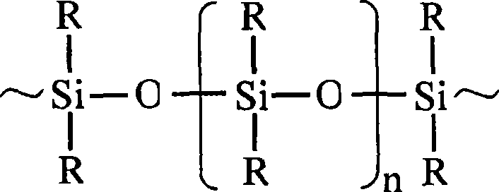
树脂优选成型前在主链上具有二甲基硅氧烷。二甲基硅氧烷是二烷基硅氧烷骨架之中的1种形态。以下的化学式2表示二甲基硅氧烷。The resin preferably has dimethylsiloxane on the main chain before molding. Dimethylsiloxane is one form of dialkylsiloxane skeleton. The following Chemical Formula 2 represents dimethylsiloxane.
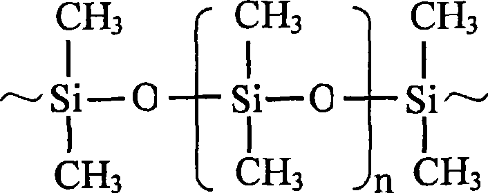
树脂在红外光谱的键吸收强度中,优选树脂组成中的C—Si—O键与Si—O—Si键的强度比为1.2/1或以上。In the bond absorption intensity of the resin in the infrared spectrum, it is preferable that the intensity ratio of the C—Si—O bond and the Si—O—Si bond in the resin composition is 1.2/1 or more.
本发明涉及一种发光装置的制造方法,其具有:将发光元件承载在基体上的第一工序;将该发光元件用无机粘结剂覆盖的第二工序;将该无机粘结剂用树脂覆盖的第三工序,其中第三工序使用浇灌手段或喷涂喷雾手段使树脂覆盖无机粘结剂。The invention relates to a method for manufacturing a light-emitting device, which comprises: a first step of carrying a light-emitting element on a substrate; a second step of covering the light-emitting element with an inorganic binder; covering the inorganic binder with a resin The third process, wherein the third process uses pouring means or spraying means to cover the resin with the inorganic binder.
第三工序优选的是在真空中进行浸渍。In the third step, it is preferable to impregnate in a vacuum.
因为具有上面所说明的构成,所以本发明产生出如下所述的效果。Because of the configuration described above, the present invention produces the following effects.
本发明涉及一种发光装置,其具有发光元件和承载该发光元件的基体,在该发光装置中,所述发光元件被无机粘结剂所覆盖,所述无机粘结剂被树脂所覆盖,以所述树脂覆盖所述无机粘结剂的步骤使用浇灌手段或喷涂喷雾手段,使所述无机粘结剂浸渍所述树脂。由此,即使在使用高输出功率的发光元件或放出紫外线的发光元件的情况下,可以提供一种树脂退化的促进受到抑制、能够长时间耐紫外线等的涂膜。另外,可以不发生覆盖发光元件的无机粘结剂的退化而谋求光取出效率的提高。再者,因为整个无机粘结剂都采用树脂来浸渍,所以无机粘结剂不会产生裂纹和缺陷,可以形成耐冲击的涂膜。The invention relates to a light-emitting device, which has a light-emitting element and a substrate carrying the light-emitting element. In the light-emitting device, the light-emitting element is covered by an inorganic binder, and the inorganic binder is covered by a resin, so that In the step of covering the inorganic binder with the resin, the resin is impregnated with the inorganic binder by pouring or spraying. Thereby, even in the case of using a high-output light-emitting element or a light-emitting element emitting ultraviolet light, it is possible to provide a coating film that is resistant to ultraviolet rays or the like for a long period of time while the promotion of resin degradation is suppressed. In addition, the light extraction efficiency can be improved without causing degradation of the inorganic binder covering the light emitting element. Furthermore, since the entire inorganic binder is impregnated with resin, the inorganic binder does not generate cracks and defects, and an impact-resistant coating film can be formed.
这是由以下作用所决定的。This is determined by the following effects.
无机粘结剂固化时,有形成空隙的部分。在现有技术中,由于该空隙的作用,光的取出受到抑制,而在本发明中,采用树脂将该空隙填埋起来,由此可谋求光取出效率的改善。When the inorganic binder is cured, there are portions where voids are formed. In the prior art, light extraction was suppressed due to the effect of the void, but in the present invention, the light extraction efficiency can be improved by filling the void with a resin.
作为采用树脂将该空隙填埋起来的手段,使用的是浇灌手段或喷涂喷雾手段。浇灌手段、喷涂喷雾手段之外的手段例如一次性地往整个无机粘结剂注入树脂的手段,要向外排出的气体或者残存在无机粘结层中,或者侵入树脂中而将气体保存下来。存在于该无机粘结层中的气体被封闭在层中,保存在层中的气体因发光装置激励时发光元件的发热而膨胀。由此,往往发生光取出效率低下的情况。与此相对照,在浇灌手段、喷涂喷雾手段中,树脂一边将无机粘结剂的空隙中含有的气体向外部挤出,一边向无机粘结剂中渗透,所以无机粘结剂的空隙中几乎没有残存气体,树脂几乎可以完全填埋无机粘结剂所具有的空隙。因此,即使在激励发光装置时,在空隙和无机粘结层界面的反射也受到抑制,不会产生光取出效率低下的情况,而涂膜本身是稳定的。As a means of filling this void with resin, pouring means or spraying means is used. For methods other than pouring and spraying, such as the method of injecting resin into the entire inorganic binder at one time, the gas to be exhausted either remains in the inorganic adhesive layer or infiltrates into the resin to preserve the gas. The gas present in the inorganic adhesive layer is enclosed in the layer, and the gas stored in the layer expands due to heat generated by the light-emitting element when the light-emitting device is activated. As a result, light extraction efficiency tends to decrease. In contrast, in the pouring method and the spraying spray method, the resin penetrates into the inorganic binder while extruding the gas contained in the voids of the inorganic binder to the outside, so the voids of the inorganic binder are almost Without residual gas, the resin can almost completely fill the voids that the inorganic binder has. Therefore, even when the light-emitting device is excited, the reflection at the interface between the void and the inorganic adhesive layer is suppressed, the light extraction efficiency does not decrease, and the coating film itself is stable.
由于无机粘结剂所具有的空隙中有柔软的有机类树脂的侵入,所以因热引起的气体的体积膨胀所导致的裂纹的发生可以受到抑制。Since the soft organic resin penetrates into the voids of the inorganic binder, the occurrence of cracks due to the volume expansion of the gas due to heat can be suppressed.
无机粘结剂优选形成有覆盖发光元件及基体的至少一部分的无机粘结层。这是因为:通过形成为层结构,能够容易地采用树脂浸渍无机粘结剂所具有的空隙。另外,从光取出的角度来看,可以几乎均匀地向外部发出源于发光元件的光。The inorganic adhesive is preferably formed with an inorganic adhesive layer covering at least a part of the light-emitting element and the substrate. This is because it is possible to easily use the resin-impregnated voids that the inorganic binder has by forming a layer structure. In addition, from the viewpoint of light extraction, light from the light emitting element can be emitted to the outside almost uniformly.
无机粘结剂优选采用树脂将无机粘结层所具有的空隙填埋起来。由此,无机粘结层的空隙消失,可以谋求光取出效率的提高。因此,所使用的树脂量仅够填埋无机粘结层的空隙就行。As the inorganic binder, it is preferable to fill voids in the inorganic binder layer with a resin. Thereby, voids in the inorganic adhesive layer disappear, and light extraction efficiency can be improved. Therefore, the amount of resin used is only enough to fill the voids of the inorganic adhesive layer.
另外,无机粘结剂优选的是可以通过树脂将无机粘结层所具有的95%或以上的空隙填埋起来。这是因为:如果只是无机粘结层所具有的空隙的一部分被树脂填埋,则空隙部分抑制光的取出。在无机粘结层离开发光元件的情况下,因为不会从发光元件直接进行热传导,所以不要特别考虑因热引起的退化,因而树脂也可以不填埋该空隙。但是,如果需要考虑源于发光元件的光,则优选采用树脂将该空隙几乎完全填埋起来。In addition, the inorganic binder is preferably capable of filling 95% or more of voids in the inorganic binder layer with the resin. This is because if only a part of the voids of the inorganic adhesive layer is filled with the resin, the voids will suppress the extraction of light. When the inorganic adhesive layer is separated from the light-emitting element, since heat conduction is not directly performed from the light-emitting element, degradation due to heat is not particularly considered, and the resin does not need to fill the gap. However, if it is necessary to consider the light from the light-emitting element, it is preferable to fill the void almost completely with a resin.
无机粘结剂优选在其中含有荧光体。由此,该荧光体吸收源于发光元件的光的一部分并进行波长转换,从而向外部发出与发光元件的光不同的光,将源于发光元件的光的一部分与源于荧光体的光的一部分混合,藉此便可以提供一种具有所希望的色调的发光装置。另外,通过设计成含有荧光体的无机粘结层,可以使色调调节变得容易,并提供一种发出均匀光线的、合格率高的发光装置。The inorganic binder preferably contains a phosphor therein. Accordingly, the phosphor absorbs part of the light from the light-emitting element and converts the wavelength to emit light different from the light from the light-emitting element to the outside, and the part of the light from the light-emitting element and the light from the phosphor A part of the mixture can thereby provide a light-emitting device with a desired color tone. In addition, by designing an inorganic adhesive layer containing a phosphor, color tone adjustment can be facilitated, and a light-emitting device that emits uniform light and has a high yield can be provided.
树脂优选的是可以形成覆盖无机粘结剂的至少一部分的树脂层。通过形成为层结构,可以形成膜厚均匀的涂膜,从而谋求光取出效率的提高。The resin is preferably capable of forming a resin layer covering at least a part of the inorganic binder. By forming a layer structure, a coating film with a uniform film thickness can be formed, and the light extraction efficiency can be improved.
树脂层的表面优选的是平滑的表面。无机粘结剂固化时,其表面存在凹凸。因此,当由发光元件发出的光透过无机粘结剂向外部发出时,由于该凹凸部分的作用,光的指向性产生偏差。与此相对照,当在无机粘结剂中浸渍树脂时,涂膜表面变得平滑,可以降低光的指向性的偏差。The surface of the resin layer is preferably a smooth surface. When the inorganic binder is cured, there are unevenness on its surface. Therefore, when the light emitted from the light-emitting element passes through the inorganic binder and is emitted to the outside, the directivity of the light is deviated due to the effect of the concave-convex portion. On the other hand, when the inorganic binder is impregnated with a resin, the surface of the coating film becomes smooth, and variations in light directivity can be reduced.
树脂优选含有油料、凝胶以及橡胶之中的至少任一种。这是为了使树脂浸渍到无机粘结剂中。特别是使用处于油料状态的树脂将树脂浸渍到无机粘结剂中的情况,因加热等而产生凝胶化,藉此可以提高一种光取出效率高的发光装置。另外,在凝胶状或橡胶状的形态中,能够容易地控制树脂的硬度。再者,与发光元件上设置的电极和外部电极进行电连接的引线,即使对树脂进行固化,引线也不会被切断。在现有技术中,当固化环氧树脂时,由于引线与环氧树脂的热膨胀系数存在差异,引线被切断。而在本发明中,由于树脂呈油料状、或者凝胶状、橡胶状,引线不会被切断。另外,单凭无机粘结剂,耐冲击能力较弱,而用呈橡胶状等的树脂填埋,藉此可以赋予涂膜以柔软性,可以形成耐冲击能力强的涂膜。The resin preferably contains at least any one of oil, gel and rubber. This is to impregnate the resin into the inorganic binder. In particular, when the resin is impregnated into the inorganic binder using a resin in an oil state, gelation occurs due to heating or the like, whereby a light-emitting device with high light extraction efficiency can be improved. In addition, in a gel-like or rubber-like form, the hardness of the resin can be easily controlled. Furthermore, the lead wires electrically connected to the electrodes provided on the light emitting element and the external electrodes are not cut even if the resin is cured. In the prior art, when the epoxy resin is cured, the lead wire is cut due to the difference in thermal expansion coefficient between the lead wire and the epoxy resin. However, in the present invention, since the resin is oily, or gelatinous, or rubbery, the lead wire will not be cut. In addition, the impact resistance of the inorganic binder alone is weak, and by filling it with a resin such as rubber, the coating film can be given flexibility and a coating film with strong impact resistance can be formed.
树脂优选在成型前及成型后的任一种情况下,是具有二烷基硅氧烷骨架的硅树脂。通过使用该树脂,可以提供一种树脂的退化进一步受到抑制、可以长时间耐紫外线等的涂膜得以使用的发光装置。The resin is preferably a silicone resin having a dialkylsiloxane skeleton both before and after molding. By using this resin, it is possible to provide a light-emitting device in which degradation of the resin is further suppressed, and a coating film that is resistant to ultraviolet rays or the like for a long period of time can be used.
树脂优选成型前在主链上具有二甲基硅氧烷。由此可以提供一种树脂的退化进一步受到抑制、可以长时间耐紫外线等的涂膜得以使用的发光装置。The resin preferably has dimethylsiloxane on the main chain before molding. Accordingly, it is possible to provide a light-emitting device in which degradation of the resin is further suppressed, and a coating film that is resistant to ultraviolet rays or the like for a long period of time can be used.
树脂在红外光谱的键吸收强度中,优选树脂组成中的C—Si—O键与Si—O—Si键的强度比为1.2/1或以上。通过设定为1.2/1或以上,由于树脂保持为油料状、或者凝胶状、橡胶状,可以形成应力得以缓和、裂纹或缺陷难以产生的涂膜。In the bond absorption intensity of the resin in the infrared spectrum, it is preferable that the intensity ratio of the C—Si—O bond and the Si—O—Si bond in the resin composition is 1.2/1 or more. By setting it at 1.2/1 or more, since the resin remains in an oily, gel-like, or rubber-like state, stress can be relaxed and a coating film in which cracks or defects hardly occur can be formed.
本发明涉及一种发光装置的制造方法,其具有:将发光元件承载在基体上的第一工序;将该发光元件用无机粘结剂覆盖的第二工序;将该无机粘结剂用树脂覆盖的第三工序,其中第三工序使用浇灌树脂的手段或对树脂进行喷涂喷雾手段来覆盖无机粘结剂。通过使用浇灌树脂的手段或对树脂进行喷涂喷雾手段,可以填埋无机粘结剂所具有的空隙。另外,可以防止该空隙中存在的气体侵入树脂之中。再者,可以稳定且均匀地涂布覆盖粘结剂的树脂。特别地,通过使用在溶胶-凝胶反应过程中不会发生价数的变化而氧化状态稳定的Al和Y元素等水合氧化物的凝胶,可以谋求光取出效率的提高。The invention relates to a method for manufacturing a light-emitting device, which comprises: a first step of carrying a light-emitting element on a substrate; a second step of covering the light-emitting element with an inorganic binder; covering the inorganic binder with a resin The third process, wherein the third process uses the means of pouring the resin or spraying the resin to cover the inorganic binder. Voids in the inorganic binder can be filled by pouring the resin or spraying the resin. In addition, it is possible to prevent the gas present in the void from intruding into the resin. Furthermore, the resin covering the adhesive can be stably and uniformly applied. In particular, the light extraction efficiency can be improved by using a gel of hydrated oxides such as Al and Y elements whose oxidation states are stable without valence change during the sol-gel reaction process.
第三工序也可以在真空中进行浸渍。由此,树脂可以容易地浸渍到无机粘结层中的空隙里。虽然其原因尚不清楚,但一般认为起因于毛细管现象。在这里,所谓“凝胶”是指由溶胶失去流动性的固体和液体构成的胶态体系。The third step may also be impregnated in a vacuum. Thereby, the resin can be easily impregnated into the voids in the inorganic adhesive layer. Although the cause thereof is not clear, it is generally considered to be caused by capillarity. Here, the so-called "gel" refers to a colloidal system composed of a solid and a liquid that have lost fluidity of the sol.
附图说明 Description of drawings
图1表示溶胶-凝胶反应的进行和发光膜的透光率的变化之间的关系。FIG. 1 shows the relationship between the progress of the sol-gel reaction and the change in the light transmittance of the luminescent film.
图2是表示本发明的实施方案1的发光装置的示意图。Fig. 2 is a schematic diagram showing a light-emitting device according to
图3是示意表示本发明的实施方案2的发光装置的平面图。Fig. 3 is a plan view schematically showing a light emitting device according to Embodiment 2 of the present invention.
图4是图3的发光装置的剖面图。FIG. 4 is a cross-sectional view of the light emitting device of FIG. 3 .
图5是本发明的又一实施方案的发光装置的示意剖面图。Fig. 5 is a schematic cross-sectional view of a light emitting device according to still another embodiment of the present invention.
图6示意表示了形成本发明的实施方案的发光装置的工序。Fig. 6 schematically shows the process of forming a light emitting device according to an embodiment of the present invention.
图7示意表示了形成本发明的实施方案的发光装置的装置。Fig. 7 schematically shows a device for forming a light emitting device according to an embodiment of the present invention.
图8是示意表示本发明的实施方案3的发光装置的平面图。Fig. 8 is a plan view schematically showing a light emitting device according to Embodiment 3 of the present invention.
图9是图8的发光装置的A—A’向剖面图。Fig. 9 is a cross-sectional view of the light emitting device of Fig. 8 along the line A-A'.
图10是示意表示本发明的实施方案4的发光装置的剖面图。Fig. 10 is a cross-sectional view schematically showing a light emitting device according to
图11是示意表示本发明的实施方案5的发光装置之制造过程的剖面图。Fig. 11 is a cross-sectional view schematically showing a manufacturing process of a light-emitting device according to Embodiment 5 of the present invention.
图12是示意表示本发明的实施方案5的发光装置之制造过程的剖面图。Fig. 12 is a cross-sectional view schematically showing a manufacturing process of a light-emitting device according to Embodiment 5 of the present invention.
图13是示意表示本发明的实施方案5的发光装置之制造过程的剖面图。Fig. 13 is a cross-sectional view schematically showing a manufacturing process of a light-emitting device according to Embodiment 5 of the present invention.
图14是示意表示本发明的实施方案5的发光装置之制造过程的剖面图。Fig. 14 is a cross-sectional view schematically showing a manufacturing process of a light-emitting device according to Embodiment 5 of the present invention.
图15是示意表示本发明的实施方案5的发光装置之制造过程的剖面图。Fig. 15 is a cross-sectional view schematically showing a manufacturing process of a light-emitting device according to Embodiment 5 of the present invention.
图16是示意表示本发明的实施方案5的发光装置之制造过程的剖面图。Fig. 16 is a cross-sectional view schematically showing a manufacturing process of a light-emitting device according to Embodiment 5 of the present invention.
图17是示意表示本发明的实施方案5的发光装置之制造过程的剖面图。Fig. 17 is a cross-sectional view schematically showing a manufacturing process of a light-emitting device according to Embodiment 5 of the present invention.
图18是示意表示本发明的实施方案5的发光装置之制造过程的剖面图。Fig. 18 is a cross-sectional view schematically showing a manufacturing process of a light-emitting device according to Embodiment 5 of the present invention.
图19是示意表示本发明的实施方案5的发光装置的剖面图。Fig. 19 is a cross-sectional view schematically showing a light emitting device according to Embodiment 5 of the present invention.
图20是示意表示本发明的实施方案5的其它发光装置的平面图。Fig. 20 is a plan view schematically showing another light-emitting device according to Embodiment 5 of the present invention.
图21是图20的发光装置的B—B’向剖面图。Fig. 21 is a cross-sectional view of the light emitting device of Fig. 20 taken along line BB'.
图22是图21的发光装置的主要部分的放大剖面图。Fig. 22 is an enlarged cross-sectional view of a main part of the light emitting device of Fig. 21 .
图23是表示本发明的实施例15~23的荧光体的色度的色度图。23 is a chromaticity diagram showing the chromaticity of phosphors in Examples 15 to 23 of the present invention.
图24是用波长365nm的LED激发本发明的实施例23的三波长白色荧光体的谱图。Fig. 24 is a spectrum diagram of the three-wavelength white phosphor of Example 23 of the present invention excited by an LED with a wavelength of 365 nm.
图25是用波长400nm的LED激发本发明的实施例19的三波长白色荧光体的谱图。Fig. 25 is a spectrum diagram of the three-wavelength white phosphor of Example 19 of the present invention excited by an LED with a wavelength of 400 nm.
图26表示本发明的实施例的荧光体的可靠性试验结果。Fig. 26 shows the results of a reliability test of phosphors according to examples of the present invention.
图27表示本发明的实施例的荧光体的可靠性试验结果。Fig. 27 shows the results of a reliability test of phosphors according to examples of the present invention.
图28表示本发明的实施例的荧光体的可靠性试验结果。Fig. 28 shows the results of a reliability test of phosphors according to examples of the present invention.
图29表示本发明的实施例的荧光体的可靠性试验结果。Fig. 29 shows the results of a reliability test of phosphors according to examples of the present invention.
图30表示本发明的实施例的荧光体的可靠性试验结果。Fig. 30 shows the results of a reliability test of phosphors according to examples of the present invention.
图31是表示本发明的实施方案6的发光装置的示意平面图。Fig. 31 is a schematic plan view showing a light emitting device according to Embodiment 6 of the present invention.
图32(a)是表示本发明的实施方案的发光装置的示意剖面图,图32(b)是放大基体凹部的示意剖面图。Fig. 32(a) is a schematic cross-sectional view showing a light-emitting device according to an embodiment of the present invention, and Fig. 32(b) is a schematic cross-sectional view showing an enlarged concave portion of a substrate.
图33是表示本发明的实施方案的发光装置之制造工序的一部分的示意图。Fig. 33 is a schematic diagram showing a part of the manufacturing process of the light-emitting device according to the embodiment of the present invention.
图34是表示本发明的实施方案的发光装置之其它制造工序的一部分的示意图。Fig. 34 is a schematic view showing part of another manufacturing process of the light-emitting device according to the embodiment of the present invention.
图35是表示本发明的实施方案的发光装置之另一个其它制造工序的一部分的示意图。Fig. 35 is a schematic diagram showing part of yet another manufacturing process of the light-emitting device according to the embodiment of the present invention.
图36(a)是放大本发明的实施方案7的发光装置之基体凹部的示意剖面图,图36(b)是表示发光装置的立体图。Fig. 36(a) is an enlarged schematic cross-sectional view of a concave portion of a substrate of a light-emitting device according to
图37(a)是放大本发明的实施方案8的发光装置之基体凹部的示意剖面图,图37(b)是表示发光装置的立体图。Fig. 37(a) is an enlarged schematic cross-sectional view of a concave portion of a substrate of a light emitting device according to
图38是表示本发明的实施方案9之发光装置的一部分的示意剖面图。Fig. 38 is a schematic cross-sectional view showing part of a light-emitting device according to Embodiment 9 of the present invention.
图39表示实施例的发光装置的耐久性试验结果。Fig. 39 shows the results of the durability test of the light-emitting device of the example.
图40表示实施例的发光装置的光取出效率的结果。FIG. 40 shows the results of the light extraction efficiency of the light emitting device of the example.
图41是表示实施例的涂膜的红外光谱图。Fig. 41 is an infrared spectrogram showing coating films of Examples.
图42是表示比较例的发光装置的示意剖面图。Fig. 42 is a schematic cross-sectional view showing a light emitting device of a comparative example.
图43是表示比较例的涂膜的红外光谱图。Fig. 43 is an infrared spectrum chart showing a coating film of a comparative example.
图44是表示本发明的实施方案10的发光装置的示意构成图。Fig. 44 is a schematic configuration diagram showing a light-emitting device according to
具体实施方式 Detailed ways
下面以附图为基础就本发明的实施方案进行说明。但是,以下所示的实施方案仅用于使本发明的技术思想具体化,是发光膜、发光装置、发光膜的制造方法以及发光装置的制造方法的例示,而并不是将本发明的发光膜、发光装置、发光膜的制造方法以及发光装置的制造方法特定为以下的内容。另外,也决不是将权利要求书所示的构件特定为实施方案的构件。而且各附图所示的构件的大小和位置关系等,为使说明变得明确,有时进行了夸张。再者,构成本发明的各要素也可以设定为用同一构件构成多个要素或用一个构件兼用多个要素的形式。Embodiments of the present invention will be described below on the basis of the drawings. However, the embodiments shown below are only for actualizing the technical idea of the present invention, and are illustrations of a light emitting film, a light emitting device, a method of manufacturing a light emitting film, and a method of manufacturing a light emitting device, and do not describe the light emitting film of the present invention. , a light-emitting device, a method for manufacturing a light-emitting film, and a method for manufacturing a light-emitting device are specified as follows. In addition, the means shown in the claims are by no means specified as the means of the embodiment. In addition, the size, positional relationship, and the like of members shown in the drawings are sometimes exaggerated for clarity of description. Furthermore, each element constituting the present invention may be configured in such a manner that a plurality of elements are constituted by the same member, or a plurality of elements are used in combination by one member.
在本发明的实施方案中,将水合氧化物的凝胶用作粘结剂。图1表示的是随着溶胶-凝胶反应的进行,在从溶胶状态经过含结晶水的凝胶、或水合氧化物和氧化物至非晶质或多晶体氧化物的过程中,发光膜的透光率和光的取出效率所发生的变化。如图1所示,在将凝胶用作粘结剂的情况下,一般可以认为随着溶胶-凝胶反应的进行,越是接近多晶体结构,发光膜的透过率像图中A所示的那样就越上升。但是,在采用溶胶-凝胶反应获得多晶体方面,需要相当多的能量。在分离凝胶状态的结构所含有的羟基和有机基团的过程中需要相当高的温度,所以并不那么容易。In an embodiment of the invention, gels of hydrous oxides are used as binders. Figure 1 shows that as the sol-gel reaction proceeds, from the sol state through the gel containing crystal water, or hydrated oxides and oxides to amorphous or polycrystalline oxides, the luminescent film Changes in light transmittance and light extraction efficiency. As shown in Figure 1, in the case of using gel as a binder, it can generally be considered that as the sol-gel reaction progresses, the closer to the polycrystalline structure, the transmittance of the luminescent film is as shown in A in the figure. As shown, it will rise more and more. However, considerable energy is required in obtaining polycrystals using sol-gel reactions. The process of separating the hydroxyl groups and organic groups contained in the structure of the gel state requires a relatively high temperature, so it is not so easy.
本发明者经过潜心的研究,结果发现:在特定的金属元素中,即使不提高结晶性,也能在凝胶状态下获得高的光取出效率,从而成就了本发明。特别地,如果使用在溶胶-凝胶反应过程中不会发生价数的变化而氧化状态稳定的Al和Y元素等水合氧化物的凝胶,则如图1中的B所示的那样,发现处于凝胶状态的光取出效率具有比溶胶-凝胶反应进行中的多晶体状态的光取出效率更高的倾向。例如在钇之类的非晶体中,一般认为其中的一个原因是由光的散射引起的。也就是说,在通过高温加热进行的结晶化阶段,在从化学结构方面来看形成多分子的从a到b的结晶化过程中,从微观方面来看,一般认为部分结晶的部分和处于凝胶状态的部分发生相分离而形成为多相结构。因此,从微观方面来看,相与相之间是不均匀的,因而在相的界面发生光的散射,从整体上说使透过率降低。作为另一项理由,一般认为是由结晶结构引起的。也就是说,在从a到b的状态下,由于以球晶的形成为基础的结晶区域和非晶区域的形成,引起各区域的密度和折射率不同。即使在微观方面是均匀的,在光学方面也形成多分子结构,因而从整体上说使透过率降低。因此,即使没有形成多晶体,也通过在凝胶状态下形成发光膜,使溶胶-凝胶反应不会继续下去而能够以短时间、低能量容易地获得光取出效率高的发光膜。As a result of intensive studies, the present inventors have found that, among specific metal elements, high light extraction efficiency can be obtained in a gel state without improving the crystallinity, thereby achieving the present invention. In particular, if a gel of hydrated oxides such as Al and Y elements whose oxidation state is stable without valence change during the sol-gel reaction is used, as shown in B in FIG. 1, it is found that The light extraction efficiency in the gel state tends to be higher than that in the polycrystalline state where the sol-gel reaction is progressing. For example, in amorphous materials such as yttrium, it is generally believed that one of the causes is the scattering of light. That is to say, in the stage of crystallization by high-temperature heating, in the crystallization process from a to b that forms multimolecules from the perspective of chemical structure, it is generally considered that the partially crystallized part and the part that is in the condensed phase are microscopically The part in the gel state undergoes phase separation to form a multiphase structure. Therefore, from a microscopic point of view, there is inhomogeneity between phases, so light scattering occurs at the interface of the phases, and the transmittance decreases as a whole. As another reason, it is generally considered to be caused by the crystal structure. That is, in the state from a to b, due to the formation of crystalline regions and amorphous regions based on the formation of spherulites, the density and refractive index of each region are different. Even if it is microscopically uniform, it will form a multi-molecular structure optically, thus lowering the transmittance as a whole. Therefore, by forming a luminescent film in a gel state even without forming polycrystals, the sol-gel reaction does not continue, and a luminescent film with high light extraction efficiency can be easily obtained in a short time and with low energy.
再者,凝胶状态为含有水合氧化物中的羟基或结晶水的状态,可以推测依其含量的不同,光取出效率将会发生变化。本发明者进行了反复的实验,结果发现:羟基或结晶水的含量占水合氧化物的10重量%或以下时,确认可以获得更高的光取出效率。这样一来,通过设定为含有结晶水的凝胶状态,可以获得致密的膜,而且与完全进行了固化的、实现了结晶化的膜相比,其光的取出效率更好。这一般认为是由于在凝胶状态下,水合氧化物具有包含部分氧化物的交联结构,提高了荧光体和元件的粘结性。In addition, the gel state is a state containing hydroxyl groups in hydrous oxides or water of crystallization, and it is presumed that the light extraction efficiency changes depending on the content thereof. As a result of repeated experiments by the present inventors, it was confirmed that higher light extraction efficiency can be obtained when the content of hydroxyl groups or water of crystallization is 10% by weight or less of the hydrous oxide. In this way, by setting the gel state containing crystal water, a dense film can be obtained, and the light extraction efficiency is better than that of a film that has been completely cured and crystallized. This is generally considered to be because in the gel state, the hydrous oxide has a cross-linked structure including some oxides, which improves the adhesion between the phosphor and the device.
另外,通过采用水合氧化物的凝胶构成粘结剂构件,可以提高形成的发光膜和发光层的品质。含有水合氧化物的粘结剂构件,其粒子状物质通过溶胶-凝胶法来聚集,从而成为形成有交联结构、网状结构或聚合物结构的多孔体。In addition, the quality of the formed luminescent film and luminescent layer can be improved by using the gel of the hydrated oxide to constitute the binder member. A binder member containing a hydrated oxide has particulate matter aggregated by a sol-gel method to form a porous body having a crosslinked structure, a network structure, or a polymer structure.
如果水合氧化物的粒子集合的骨架结构是具有孔隙的网状结构,则因为是多孔性的结构体而可以提高发光膜的柔软性。另外,发光层在成膜时,即使附载着荧光体粒子等填料构件,同时被涂覆的对象形状复杂,也可以与此相适应进行成膜,可以获得富有粘结性的发光膜。再者,由于是水合氧化物,因而可以获得对热和光稳定且不变质的膜。If the skeleton structure of the particle assembly of the hydrous oxide is a network structure having pores, the flexibility of the luminescent film can be improved because it is a porous structure. In addition, even if filler members such as phosphor particles are attached during film formation of the luminescent layer, and the object to be coated has a complex shape, the film can be formed accordingly, and a luminescent film with high adhesion can be obtained. Furthermore, since it is a hydrous oxide, a film that is stable against heat and light and does not deteriorate can be obtained.
形成的发光膜因为曝露在源于发光元件的光中,所以通过发光装置的使用而产生退化。一般认为该退化的原因在于:因源于发光元件的光输出功率和发热之中的任一种或两者而导致反应的发生。因此,当将光能量高的紫外线用于发热以及热阻抗值大的大型元件时,就容易产生退化。正如后面所叙述的那样,制作本发明的实施例的试样进行了耐久试验,结果确认具有极高的耐性。虽然其理由尚不明确,但一般认为原因在于选择了这样一种结构,即具有恒定价数的水合氧化物在热能和光能的作用下,难以发生氧化还原反应。因此,优选利用在水合氧化物中价数不会发生变化的金属元素。例如,在使用可以取得多种离子价态的Si等作为凝胶或固化膜的情况下,可以推测因光密度和由元件的发热产生的热传导而容易引起价数的变化,因而导致着色退化的产生。与此相对照,以本发明的实施方案得到的3价水合氧化物为粘结剂的发光层,则难以发生氧化还原反应。因此,本发明的发光装置即使在接触或靠近光照射密度例如为0.1W/cm2~1000W/cm2的高输出功率的半导体发光元件的情况下,也可以具有充分的耐性。Since the formed light-emitting film is exposed to light from the light-emitting element, it is degraded by use of the light-emitting device. It is generally considered that the cause of this degradation is the occurrence of a reaction due to either or both of light output power and heat generation from the light-emitting element. Therefore, when ultraviolet rays with high light energy are used for large components that generate heat and have high thermal resistance values, degradation is likely to occur. As will be described later, samples of examples of the present invention were prepared and subjected to durability tests, and as a result, it was confirmed that they had extremely high durability. Although the reason for this is not clear, it is generally believed that the reason is that such a structure is selected that a hydrated oxide having a constant valence is less likely to undergo redox reactions under the action of thermal energy and light energy. Therefore, it is preferable to use a metal element whose valence does not change in the hydrous oxide. For example, in the case of using Si, etc., which can obtain various ion valence states, as a gel or a cured film, it is presumed that the change in valence is likely to occur due to optical density and heat conduction due to heat generation of the element, thereby causing coloring deterioration. produce. In contrast, in the light-emitting layer using the trivalent hydrated oxide obtained in the embodiment of the present invention as a binder, oxidation-reduction reactions hardly occur. Therefore, the light-emitting device of the present invention can have sufficient resistance even when it is in contact with or close to a high-output semiconductor light-emitting element with a light irradiation density of, for example, 0.1 W/cm 2 to 1000 W/cm 2 .
(粘结剂)(binder)
作为附载着在高温下或紫外线激发下使用的荧光体的粘结剂,所采用的是二氧化硅(SiO2)。当继续使用二氧化硅粘结剂时,混合有对发光元件的发光进行转换的荧光体和透光性材料的荧光构件慢慢黑化。本发明者研究了这样的着色退化的原因,结果查明:其原因在于在二氧化硅粘结层中产生氧的缺损而生成了SiOX(x<2)。Silica (SiO 2 ) is used as a binder for attaching phosphors used under high temperature or ultraviolet excitation. As the silica binder continues to be used, the fluorescent member in which the fluorescent substance that converts the light emission of the light-emitting element and the light-transmitting material are mixed gradually blackens. The inventors of the present invention studied the cause of such deterioration of coloration, and as a result, found that the cause is generation of SiO X (x<2) due to oxygen deficiency in the silica adhesive layer.
二氧化硅粘结剂在250℃或以下的热固化温度下,呈二氧化硅凝胶状,在SiO2骨架中残存一部分羟基和有机基团。在这样的二氧化硅凝胶的状态下,当由LED入射高密度的光时,则由光能或热能产生氧的缺损,从而由SiO2生成SiOX(x<2:x为1.4~1.9左右)。一般认为因该SiOX被着色而产生黑化。这样,二氧化硅凝胶一般认为是因为成为主体的金属元素Si可以取得各种价数,Si容易产生价数的变化而发生氧化还原,从而产生着色退化。于是,在本发明的实施方案中,使用含有金属元素不会发生价数变化的水合氧化物或氧化物的粘结剂。下面就利用氧化铝、氧化钇的实例进行说明。The silica binder is in the form of silica gel at a thermal curing temperature of 250°C or below, and a part of hydroxyl groups and organic groups remain in the SiO2 skeleton. In the state of such a silica gel, when high-density light is incident from the LED, oxygen vacancies are generated by light energy or thermal energy, thereby generating SiO X from SiO 2 (x<2: x is 1.4 to 1.9 about). It is generally considered that the SiO X is colored to cause blackening. In this way, silica gel is generally considered to be because Si, the main metal element, can take various valences, and Si tends to change in valence to cause oxidation and reduction, thereby causing coloring degradation. Therefore, in an embodiment of the present invention, a binder containing a hydrated oxide or an oxide in which a metal element does not change in valence is used. An example using alumina and yttrium oxide will be described below.
(氧化铝)(alumina)
将无定形氧化铝或微粒子水合氧化铝均匀分散在水中,并将这样形成的氧化铝溶胶用作粘结剂,在这种情况下,在加热氧化铝溶胶而固化形成为具有稳定的勃姆石结构的水合氧化铝之前,经历一个伪勃姆石结构的阶段。水合氧化铝的勃姆石结晶结构和水合氧化铝的伪勃姆石结构可以分别用化学式AlOOH或Al2O3·H2O和(AlOOH)·xH2O或Al2O3·2H2O等来表示。具体地说,作为中间体取Al2O3·2H2O、Al2O3·xCH3COOH·yH2O、Al2O3·xHCl·yH2O、Al2O3·xHNO3·yH2O等形态,最后形成稳定的勃姆石结构。进一步提高勃姆石结构的结晶性,则成为γ-氧化铝(Al2O3)或α-氧化铝(Al2O3)。将具有这样性质的氧化铝溶胶用作粘结剂,从而形成发光膜。Amorphous alumina or microparticle hydrated alumina is uniformly dispersed in water, and the alumina sol thus formed is used as a binder, in this case, the alumina sol is heated and solidified to form a stable boehmite Before the structure of the hydrated alumina, it undergoes a stage of pseudo-boehmite structure. The boehmite crystal structure of hydrated alumina and the pseudo-boehmite structure of hydrated alumina can be represented by the chemical formula AlOOH or Al 2 O 3 ·H 2 O and (AlOOH)·xH 2 O or Al 2 O 3 ·2H 2 O wait to express. Specifically, Al 2 O 3 ·2H 2 O, Al 2 O 3 ·xCH 3 COOH ·yH 2 O, Al 2 O 3 ·xHCl·yH 2 O, Al 2 O 3 ·xHNO 3 ·yH 2 O and other forms, finally forming a stable boehmite structure. If the crystallinity of the boehmite structure is further improved, it becomes γ-alumina (Al 2 O 3 ) or α-alumina (Al 2 O 3 ). An alumina sol having such properties is used as a binder, thereby forming a light emitting film.
作为发光膜的具体的主材料,可以使用按如下方法制备的溶胶溶液,即以少量的无机酸、有机酸以及碱为稳定剂,将无定形金属氧化物、超微粒子金属水合氧化物以及超微粒子氧化物等均匀分散在水或有机溶剂中。作为合成无定形金属氧化物、超微粒子金属水合氧化物以及超微粒子氧化物等的初始原料,可以利用的有:烷氧基金属、双二酮基金属(metal diketonate)、金属卤化物、或金属羧酸盐、金属烷基化合物的水解产物以及将它们混合后进行水解的产物。另外,也可以使用将金属氢氧化物、金属氯化物、金属硝酸盐以及金属氧化物微粒子均匀分散在水和有机溶剂、或者水和水溶性有机溶剂的混合溶剂中所制备的胶体(溶胶)溶液。它们总称为铝氧烷。铝氧烷的骨架中具有[AlO]X的重复单元。As the specific main material of the luminescent film, a sol solution prepared by the following method can be used, that is, a small amount of inorganic acid, organic acid and alkali are used as stabilizers, and amorphous metal oxides, ultrafine metal hydrated oxides and ultrafine particles Oxides, etc. are uniformly dispersed in water or organic solvents. As the starting materials for the synthesis of amorphous metal oxides, ultrafine metal hydrated oxides, and ultrafine particle oxides, metal alkoxides, metal diketonates, metal halides, or metal oxides can be used. Hydrolyzed products of carboxylate and metal alkyl compounds, and hydrolyzed products after mixing them. In addition, a colloid (sol) solution prepared by uniformly dispersing metal hydroxides, metal chlorides, metal nitrates, and metal oxide fine particles in water and an organic solvent, or a mixed solvent of water and a water-soluble organic solvent can also be used. . They are collectively referred to as aluminoxanes. Aluminoxane has a repeating unit of [AlO] X in its skeleton.
作为烷氧基金属,可以利用的有:甲氧基铝、乙氧基铝、正丙氧基铝、异丙氧基铝、正丁氧基铝、仲丁氧基铝、异丙氧基铝、叔丁氧基铝、甲氧基钇、乙氧基钇、正丙氧基钇、异丙氧基钇、正丁氧基钇、仲丁氧基钇、异丙氧基钇、叔丁氧基钇等。As the metal alkoxide, there are: aluminum methoxide, aluminum ethoxide, aluminum n-propoxide, aluminum isopropoxide, aluminum n-butoxide, aluminum sec-butoxide, aluminum isopropoxide , tert-butoxy aluminum, methoxy yttrium, ethoxy yttrium, n-propoxy yttrium, isopropoxy yttrium, n-butoxy yttrium, sec-butoxy yttrium, isopropoxy yttrium, tert-butoxy Yttrium etc.
作为双二酮基金属,可以利用的有:三乙基乙酰乙酸铝、烷基乙酰乙酸二异丙氧基铝、乙基乙酰乙酸二异丙氧基铝、单乙酰基丙酮酸双乙基乙酰乙酸铝、三乙酰基丙酮酸铝、三乙酰基丙酮酸钇以及三乙基乙酰乙酸钇等。As bis-diketonate metals, available are: aluminum triethylacetoacetate, diisopropoxyaluminum alkylacetoacetate, diisopropoxyaluminum ethylacetoacetate, diethylacetylacetonate monoacetylacetonate Aluminum acetate, aluminum triacetylacetonate, yttrium triacetylacetonate, and yttrium triethylacetoacetate.
作为金属羧酸盐,可以利用的有:醋酸铝、丙酸铝、2-乙基己酸铝、醋酸钇、丙酸钇以及2-乙基己酸钇等。Usable metal carboxylates include aluminum acetate, aluminum propionate, aluminum 2-ethylhexanoate, yttrium acetate, yttrium propionate, and yttrium 2-ethylhexanoate.
另外,作为金属卤化物,可以利用的有:氯化铝、溴化铝、碘化铝、氯化钇、溴化钇以及碘化钇等。In addition, as metal halides, aluminum chloride, aluminum bromide, aluminum iodide, yttrium chloride, yttrium bromide, yttrium iodide, and the like can be used.
作为有机溶剂,可以利用的有:甲醇、乙醇、正丙醇、异丙醇、正丁醇、仲丁醇、叔丁醇、四氢呋喃、二噁烷、丙酮、乙二醇、甲乙酮、N,N-二甲基甲酰胺以及N,N-二甲基乙酰胺等。As an organic solvent, methanol, ethanol, n-propanol, isopropanol, n-butanol, sec-butanol, tert-butanol, tetrahydrofuran, dioxane, acetone, ethylene glycol, methyl ethyl ketone, N, N -Dimethylformamide and N,N-dimethylacetamide, etc.
作为形成发光层的粘结剂加以使用的除了这些以外,也可以混合作为填料的荧光体和扩散粒子。再者,作为它们的复合体,也可以使基体和发光元件的线膨胀系数保持一致。作为填料,混入荧光体而产生发光自不必说,同时还产生出固化时的水分蒸发等的微细通路,具有加快粘结剂的固化干燥的效果。另外,还具有将荧光体的发光扩散开来、增加发光层的粘结强度和物理强度的作用。此外,发光层和发光膜也可以作为不含荧光体的扩散层加以使用。另外,在作为粘结剂加以使用的复合材料中,除3价金属元素以外,也可以少量含有具有多种价数的元素。再者,粘结剂构件可以包含水合氧化物作为主要的化合物,即使包含一部分金属氧化物和金属氢氧化物以及它们的结合也可以发挥作用。In addition to these used as a binder for forming the light emitting layer, phosphors and diffusing particles as fillers may be mixed. Furthermore, as a composite of these, the coefficients of linear expansion of the substrate and the light-emitting element can also be made the same. As a filler, it is not only necessary to mix phosphors to produce light emission, but also to create fine channels for moisture evaporation during curing, which has the effect of accelerating the curing and drying of the adhesive. In addition, it also has the function of diffusing the luminescence of the phosphor and increasing the bonding strength and physical strength of the luminescent layer. In addition, a light emitting layer and a light emitting film can also be used as a diffusion layer not containing a phosphor. In addition, the composite material used as a binder may contain a small amount of elements having various valences in addition to trivalent metal elements. Furthermore, the binder member may contain a hydrated oxide as a main compound, and may function even if it contains a part of metal oxide and metal hydroxide and combinations thereof.
(填料)(filler)
填料就是填充剂,可以利用的有:钛酸钡、氧化钛、氧化铝(三氧化二铝)、氧化钇(三氧化二钇)、二氧化硅、碳酸钙以及其它水合氧化物等。例如,也可以有相对于至少包含选自Al、Ga、Ti、Gc、P、B、Zr、Y或碱土金属之中的一种或多种元素的无色水合氧化物、或至少包含选自Si、Al、Ga、Ti、Ge、P、B、Zr、Y或碱土金属之中的一种或多种元素的氧化物具有更高热传导系数的填料。通过添加这样的填料,发光装置的排热效果得以提高。作为这样的填料,在采用上述无机粘结剂形成粘结层而对LED芯片进行芯片焊接(die bond)时,可以列举出氧化铝、Ag等金属粉。Fillers are fillers, which can be used: barium titanate, titanium oxide, aluminum oxide (aluminum oxide), yttrium oxide (yttrium oxide), silicon dioxide, calcium carbonate, and other hydrated oxides. For example, there may also be a colorless hydrated oxide containing at least one or more elements selected from Al, Ga, Ti, Gc, P, B, Zr, Y, or alkaline earth metals, or at least containing one or more elements selected from Oxides of one or more elements among Si, Al, Ga, Ti, Ge, P, B, Zr, Y or alkaline earth metals have higher thermal conductivity fillers. By adding such fillers, the heat removal effect of the light emitting device can be improved. Examples of such fillers include metal powders such as alumina and Ag when forming an adhesive layer using the above-mentioned inorganic binder and performing die bonding on an LED chip.
在粘结剂的溶胶中,除荧光体及低级醇之外,通过事先混合分散剂,可以借助于固化时与低级醇的共沸脱水在低温形成致密的涂膜。另外,也可以含有光稳定化材料、着色剂以及紫外线吸收剂等。In the sol of the binder, besides the phosphor and the lower alcohol, by mixing the dispersant in advance, a dense coating film can be formed at low temperature by means of azeotropic dehydration with the lower alcohol during curing. In addition, photostabilizers, colorants, ultraviolet absorbers, and the like may be contained.
进而在形成发光膜时,也可以添加硼酸和氧化硼。由于硼酸和氧化硼的添加,导致发光膜的弹性降低,所以膜的品质得以提高。例如可以抑制发光膜的裂纹的产生并形成致密的膜。硼酸和氧化硼相对于粘结剂构件优选含有0.5重量%~50重量%。再者,在发光膜中,也可以添加除硼酸和氧化硼以外的增粘剂。这样一来,作为粘结剂构件,除铝等水合氧化物以外,也可以含有用于控制料浆粘度的添加剂。因此,在成膜时控制粘度、提高触变性,便可以成形出形状复杂的膜。另外,在膜形成后,由于粘结剂是水合氧化物,因而可以提高对添加剂的许用能力,而且可以在控制粘结剂结构体的结构方面发挥作用。Furthermore, boric acid and boron oxide may be added when forming the luminescent film. Due to the addition of boric acid and boron oxide, the elasticity of the luminescent film is reduced, so the quality of the film is improved. For example, it is possible to suppress the occurrence of cracks in the luminescent film and form a dense film. Boric acid and boron oxide are preferably contained in an amount of 0.5% by weight to 50% by weight relative to the binder member. In addition, a tackifier other than boric acid and boron oxide may be added to the luminescent film. In this way, the binder member may contain additives for controlling the viscosity of the slurry in addition to hydrated oxides such as aluminum. Therefore, by controlling viscosity and improving thixotropy during film formation, films with complex shapes can be formed. In addition, after the film is formed, since the binder is a hydrous oxide, the tolerance to additives can be improved, and it can also play a role in controlling the structure of the binder structure.
发光层用料浆溶液来形成。料浆溶液是这样调制而成的,即以无定形金属水合氧化物、微粒子金属水合氧化物以及金属氢氧化物为主要成分,将该主要成分进而将无定形金属氧化物、微粒子金属氧化物均匀分散在水中,由此制得溶胶溶液,然后在该溶胶溶液中,混合荧光体和填料。溶胶溶液中的有效固体成分与荧光体的重量比、或者溶胶溶液中的有效固体成分与荧光体和填料混合物的重量比优选为0.05~30。例如可以在相对于20g有效固体成分浓度为15%的溶胶溶液、荧光体为90g到相对于600g有效固体成分浓度为15%的溶胶溶液、荧光体为4.5g的比率范围内进行调整。The light emitting layer is formed using a slurry solution. The slurry solution is prepared by using amorphous metal hydrated oxide, fine particle metal hydrated oxide, and metal hydroxide as the main components, and the main components are further mixed with amorphous metal oxide and fine particle metal oxide. Dispersed in water, thereby preparing a sol solution, and then mixing the phosphor and the filler in the sol solution. The weight ratio of the effective solid component in the sol solution to the phosphor, or the weight ratio of the effective solid component in the sol solution to the phosphor and the filler mixture is preferably 0.05-30. For example, the ratio can be adjusted within a range from 90 g of phosphor to 20 g of a sol solution with an effective solid concentration of 15% to 4.5 g of phosphor to 600 g of a sol solution with an effective solid concentration of 15%.
(氧化钇)(yttrium oxide)
将无定形氧化钇或微粒子氧化钇均匀分散在水中,并将这样形成的氧化钇溶胶用作粘结剂,在这种情况下,即使加热固化氧化钇溶胶,结晶结构的主体也是无定形。水合氧化钇和氧化钇可以分别用YOOH·xH2O和Y2O3·xH2O等化学式来表示。具体地说,作为中间体,经过YOOH·xCH3COOH·yH2O或Y2O3·xCH3COOH·yH2O的形态,最后形成为部分含有水合氧化钇或氧化钇的形式。氧化钇即使在这样的凝胶状态下也可以形成稳定的膜。一般认为其原因在于各自的成分具有交联结构,可以实现稳定化。In the case where amorphous yttrium oxide or fine particle yttrium oxide is uniformly dispersed in water, and the yttrium oxide sol thus formed is used as a binder, even if the yttrium oxide sol is heat-cured, the main body of the crystalline structure is amorphous. Hydrated yttrium oxide and yttrium oxide can be represented by chemical formulas such as YOOH·xH 2 O and Y 2 O 3 ·xH 2 O, respectively. Specifically, as an intermediate, it passes through the form of YOOH·xCH 3 COOH·yH 2 O or Y 2 O 3 ·xCH 3 COOH·yH 2 O, and finally becomes a form partially containing hydrated yttrium oxide or yttrium oxide. Yttrium oxide can form a stable film even in such a gel state. The reason for this is considered to be that each component has a cross-linked structure, which enables stabilization.
氧化钇与氧化铝相比,具有难以形成结晶结构的性质。这样一来,即使是不具结晶性的无定形的非晶结构也可以是稳定的化合物,Y保持3价不变而不会发生价数的变化。即具有的长处是难以发生氧化还原反应,没有着色退化。Yttrium oxide has a property that it is difficult to form a crystal structure compared with alumina. In this way, even an amorphous non-crystalline structure having no crystallinity can be a stable compound, and the valency of Y remains unchanged without changing the valence number. That is, it has the advantage that oxidation-reduction reaction hardly occurs and there is no color degradation.
关于其它,则是与上述的氧化铝一样地形成发光层。正如以上所叙述的那样,荧光体作为粘结剂加以使用的溶胶,也可以利用市售的无机系粘结剂和陶瓷粘结剂等。此外,在可以作为粘结剂加以利用的材质中,并不限于氧化铝和氧化钇之类的含有Al和Y元素的水合氧化物,也可以利用其它的IIIA族元素和IIIB族元素的水合氧化物、氧化物以及氢氧化物等。选择的金属元素优选不会发生价数变化。特别地,优选的是表现为3价且稳定的金属元素。另外,也优选是无色透明的。例如除Al和Y之外,还可以利用包含Gd、Lu、Sc、Ga以及In等金属元素的金属化合物,优选可以利用Sc和Lu。或者也可以利用将多种的这些元素进行组合的复合氧化物和复合水合氧化物。不单是铝和钇,通过含有其它III族元素的水合氧化物等,也可以将发光膜的折射率等光学性能以及膜的柔软性、粘结性等膜的物性之类的各种特性控制为所希望的值。这样一来,通过具有由本发明的实施方案得到的含有价数恒定、优选为3价的水合氧化物凝胶的无机粘结剂,所形成的发光层可以设计为稳定、光取出效率良好的发光层。另外,由于用无机材料构成,因此可以制成不随时间变化的、稳定的发光层与发光膜。For the rest, the light-emitting layer is formed in the same manner as the above-mentioned alumina. As described above, commercially available inorganic binders, ceramic binders, and the like can be used as the sol in which the phosphor is used as a binder. In addition, among the materials that can be used as binders, they are not limited to hydrated oxides containing Al and Y elements such as alumina and yttrium oxide, and hydrated oxides of other IIIA group elements and IIIB group elements can also be used. compounds, oxides, and hydroxides. The selected metal element preferably does not change in valence. In particular, trivalent and stable metal elements are preferable. In addition, it is also preferably colorless and transparent. For example, in addition to Al and Y, metal compounds containing metal elements such as Gd, Lu, Sc, Ga, and In can also be used, preferably Sc and Lu can be used. Alternatively, composite oxides and composite hydrated oxides in which multiple types of these elements are combined can also be used. Not only aluminum and yttrium, but also various properties such as optical properties such as the refractive index of the luminescent film and physical properties of the film such as film flexibility and adhesiveness can be controlled by hydrated oxides containing other group III elements. desired value. In this way, by having an inorganic binder containing a hydrated oxide gel having a constant valence, preferably trivalent, obtained by the embodiment of the present invention, the formed light-emitting layer can be designed to be stable and have a high light extraction efficiency. layer. In addition, since it is composed of inorganic materials, it is possible to produce stable light-emitting layers and light-emitting films that do not change over time.
实施方案1
下面采用图2就本发明的实施方案1的发光装置进行说明。实施方案1的发光装置包括:发光元件10,由荧光体11a和包含荧光体11a的透光性粘结剂11b构成的荧光构件11。Next, a light-emitting device according to
用炮弹型的LED构成的发光元件10焊接在罩体(cup)的大致中央部位并由该罩体所承载,其中罩体配置在管脚引线(mount lead)13a的上部。发光元件10上形成的电极通过导电性引线14与引线框(leadframe)13的管脚引线13a以及内部引线(inner lead)13b进行电连接。荧光体11a含有YAG系荧光体和氮化物系荧光体,这些荧光体吸收发光元件10发出的光的至少一部分,同时发出不同于吸收光波长的光。再者,氮化物系荧光体可以用微胶囊等覆盖材料覆盖起来。在粘结剂11b中含有该荧光体11a的荧光构件11配置在承载发光元件10的罩体上。这样,为了保护LED芯片和荧光体免受外部应力、水分以及尘垢的侵害,以及为了改善光的取出效率,配置发光元件10和荧光构件11的引线框13被模压在铸模构件15中,从而形成发光装置。这样一来,在形成含有由水合氧化物构成的粘结剂的发光层后,也可以以树脂制铸模的形式形成透镜等。A light-emitting
(发光元件)(light emitting element)
在本说明书中,所谓发光元件除半导体发光元件以外,还包括用于获得由真空放电产生的发光、以及由热发光产生的发光的元件。例如,由真空放电产生紫外线等的元件也可以用作发光元件。在本发明的实施方案中,作为所利用的发光元件,其波长为550nm或以下,优选为460nm或以下,进一步优选为410nm或以下。例如可以加以利用的有:作为紫外光发出波长为250nm~365nm的光的紫外光LED和波长为253.7nm的高压水银灯。特别地,正如后面所叙述的那样,本发明的实施例所具有的优点是:耐久性优良,可以适用输出功率大的动力型发光元件。In this specification, the light-emitting element includes, in addition to semiconductor light-emitting elements, elements for obtaining light emission by vacuum discharge and light emission by thermoluminescence. For example, an element that generates ultraviolet rays or the like by vacuum discharge can also be used as a light emitting element. In an embodiment of the present invention, the light-emitting element used has a wavelength of 550 nm or less, preferably 460 nm or less, more preferably 410 nm or less. For example, an ultraviolet light LED which emits light with a wavelength of 250 nm to 365 nm as ultraviolet light and a high-pressure mercury lamp with a wavelength of 253.7 nm can be used. In particular, as will be described later, the embodiments of the present invention have advantages in that they are excellent in durability and can be applied to dynamic light-emitting elements with high output power.
下面说明将III族氮化物系半导体发光元件用作发光元件10的实例。发光元件10例如是在蓝宝石基板上、隔着GaN缓冲层依次层叠下列层所形成的层叠结构,这些层依次为:未掺杂Si或Si浓度低的第1n型GaN层;由掺杂Si或Si浓度比第1n型GaN层更高的n型GaN构成的n型接触层;未掺杂或Si浓度比n型接触层更低的第2GaN层;多重量子阱结构的发光层(GaN阻挡层/InGaN阱层的量子阱结构);由P型GaN构成的p包层,其中P型GaN由掺杂Mg的P型GaN构成;由掺杂Mg的P型GaN构成的P型接触层。并按下述的方法形成电极。当然,也可以使用不同于该构成的发光元件。An example in which a Group III nitride-based semiconductor light-emitting element is used as the light-emitting
p欧姆电极几乎在p型接触层的整个面上形成,在一部分该P欧姆电极上形成p焊盘电极(pad electrode)。The p-ohmic electrode is formed on almost the entire surface of the p-type contact layer, and a p-pad electrode (pad electrode) is formed on a part of the p-ohmic electrode.
另外,通过浸蚀从P型接触层除去第1 GaN层而露出n型接触层的一部分,n电极便在该露出部分上形成。In addition, the first GaN layer is removed from the p-type contact layer by etching to expose a part of the n-type contact layer, and the n-electrode is formed on the exposed part.
此外,本实施方案使用多重量子阱结构的发光层,但本发明并不限定于此,例如利用InGaN的单量子阱结构和多重量子阱结构都可以,也可以利用掺杂Si和Zn的GaN。In addition, this embodiment uses a light-emitting layer with a multiple quantum well structure, but the present invention is not limited thereto. For example, both a single quantum well structure and a multiple quantum well structure of InGaN can be used, and GaN doped with Si and Zn can also be used.
另外,发光元件10的发光层通过改变In的含量,可以在420nm~490nm的范围内改变主发光峰。而且发光波长并不限于上述范围,可以使用发光波长为360nm~550nm的发光元件。特别地,当将本发明的实施方案的发光装置适用于紫外光LED发光装置时,可以提高激发光的吸收转换效率,可以降低紫外光的透过。In addition, by changing the In content of the light-emitting layer of the light-emitting
(荧光体)(phosphor)
荧光体将从发光元件发出的可见光和紫外光转换为其它波长的发光。例如,用从LED的半导体发光层发出的光进行激发以产生其它波长的发光。作为优选的荧光体,可以利用的有:YAG系、碱土类氮化硅荧光体等氮化物系、碱土类氧化氮化硅荧光体等氧氮化物系。在本实施方案中,作为荧光体使用的是由紫外光激发产生预定颜色的光的荧光体。具体地说,可以利用的荧光体举例如下:The phosphor converts visible light and ultraviolet light emitted from the light emitting element into light emission of other wavelengths. For example, excitation is performed with light emitted from the semiconductor light emitting layer of the LED to generate light emission at other wavelengths. Usable phosphors include YAG-based, nitride-based phosphors such as alkaline-earth silicon nitride phosphors, and oxynitride-based phosphors such as alkaline-earth silicon oxynitride phosphors. In the present embodiment, a phosphor that is excited by ultraviolet light to generate light of a predetermined color is used as the phosphor. Specifically, examples of phosphors that can be used are as follows:
(1)Ca10(PO4)6FCl:Sb,Mn(1) Ca 10 (PO 4 ) 6 FCl:Sb, Mn
(2)M5(PO4)3Cl:Eu(其中:M为选自Sr、Ca、Ba以及Mg之中的至少一种)(2) M 5 (PO 4 ) 3 Cl:Eu (wherein: M is at least one selected from Sr, Ca, Ba and Mg)
(3)BaMg2Al16O27:Eu(3) BaMg 2 Al 16 O 27 :Eu
(4)BaMg2Al16O27:Eu,Mn(4) BaMg 2 Al 16 O 27 :Eu, Mn
(5)3.5MgO·0.5MgF2·GeO2:Mn(5) 3.5MgO·0.5MgF 2 ·GeO 2 : Mn
(6)Y2O2S:Eu(6)Y 2 O 2 S:Eu
(7)Mg6As2O11:Mn(7)Mg 6 As 2 O 11 :Mn
(8)Sr4Al14O25:Eu(8) Sr 4 Al 14 O 25 :Eu
(9)(Zr、Cd)S:Cu(9)(Zr,Cd)S:Cu
(10)SrAl2O4:Eu(10)SrAl 2 O 4 :Eu
(11)Ca10(PO4)6ClBr:Mn,Eu(11) Ca 10 (PO 4 ) 6 ClBr:Mn, Eu
(12)Zn2GeO4:Mn(12)Zn 2 GeO 4 :Mn
(13)Gd2O2S:Eu(13)Gd 2 O 2 S:Eu
(14)La2O2S:Eu(14) La 2 O 2 S:Eu
(15)Ca2Si5N8:Eu(15)Ca 2 Si 5 N 8 :Eu
(16)Sr2Si5N8:Eu(16)Sr 2 Si 5 N 8 :Eu
(17)SrSi2O2N2:Eu(17)SrSi 2 O 2 N 2 :Eu
(18)BaSi2O2N2:Eu(18) BaSi 2 O 2 N 2 :Eu
另外,除上述荧光体以外,毫无疑问,也可以利用产生黄色区域的发光的、用(Y,Gd)3(Al,Ga)5O12:Ce等表示的稀土类铝酸盐即YAG系荧光体。In addition to the above-mentioned phosphors, YAG-based rare-earth aluminates represented by (Y, Gd) 3 (Al, Ga) 5 O 12 : Ce, etc., which emit light in the yellow region, can of course also be used. Phosphor.
当LED芯片发出的光和荧光体发出的光成互补颜色关系等时,通过将各自的光混色便可以发出白色的光。具体地说,可以列举出LED芯片发出的光和由该光激发而发光的荧光体的光分别相当于3原色(红色系、绿色系、蓝色系)的情况、以及LED芯片发出的蓝色光和由该光激发而发光的荧光体的黄色光。特别是在使用紫外光的情况下,因为可以单独利用由紫外光激发发光的荧光体的发光颜色,因而获得信号用的蓝绿色、黄红色、红色等以及浅色等各种中间色的发光装置也是可能的。When the light emitted by the LED chip and the light emitted by the phosphor have a complementary color relationship, white light can be emitted by mixing the respective lights. Specifically, the light emitted by the LED chip and the light of the phosphor excited by the light correspond to the three primary colors (red, green, and blue) and the blue light emitted by the LED chip. and the yellow light of the fluorescent substance excited by this light. Especially in the case of using ultraviolet light, because the emission color of the phosphor excited by ultraviolet light can be used alone, various intermediate color light-emitting devices such as blue-green, yellow-red, red, etc. and light colors for signals can be obtained. It is also possible.
通过对作为荧光体与荧光体之间的粘结剂发挥作用的各种树脂和玻璃等无机粘结构件、与填料等的比率、荧光体的沉降时间、荧光体的形状等进行各种调整以及对LED芯片的发光波长进行选择,发光装置的发光颜色可以提供灯泡颜色(electric bulb color)等任意的白色系的色调。在发光装置的外部,优选LED芯片发出的光和和荧光体发出的光有效地透过铸模构件。By adjusting the ratio of various resins and inorganic bonding members such as glass and fillers, the sedimentation time of phosphors, the shape of phosphors, etc., which function as a binder between phosphors, and By selecting the light emission wavelength of the LED chip, the light emission color of the light emitting device can provide any white tone such as electric bulb color. On the outside of the light-emitting device, it is preferable that the light emitted from the LED chip and the light emitted from the phosphor efficiently pass through the mold member.
作为有代表性的荧光体,可以列举出用铜活化的硫化镉锌和用铈活化的YAG系荧光体。特别在高辉度且长时间使用时,优选的是(Re1-xSmX)3(Al1-yGay)5O12:Ce(0≤x<1,0≤y≤1,其中:Re是选自Y、Gd、La以及Lu之中的至少一种元素。Typical phosphors include copper-activated cadmium zinc sulfide and cerium-activated YAG-based phosphors. Especially for high luminance and long-term use, (Re 1-x Sm X ) 3 (Al 1-y Ga y ) 5 O 12 :Ce(0≤x<1, 0≤y≤1, where : Re is at least one element selected from Y, Gd, La and Lu.
(Re1-xSmX)3(Al1-yGay)5O12:Ce荧光体因为是石榴石结构,所以对热、光以及水分具有很强的耐性,激发谱峰可以达到470nm左右。另外,也可能具有宽的发光谱,其发光峰在530nm附近,峰的末端延伸到720nm处。(Re 1-x Sm X ) 3 (Al 1-y Ga y ) 5 O 12 : Ce phosphor has a garnet structure, so it has strong resistance to heat, light and moisture, and the excitation peak can reach about 470nm . In addition, it may also have a broad emission spectrum, the emission peak of which is around 530nm, and the end of the peak extends to 720nm.
在本发明的实施方案的发光装置中,荧光体也可以是2种或更多种荧光体混合而成的。即可以将2种或更多种Al、Ga、Y、La、Lu以及Gd和Sm的含量不同的(Re1-xSmX)3(Al1-yGay)5O12:Ce荧光体进行混合,从而增加RGB的波长成分。另外,使用具有黄~红色发光的氮化物荧光体等增加红色的成分,也可以获得平均演色评价指数高的照明或灯泡颜色的LED等。具体地说,混配发光元件的发光波长,调整CIE色度图上的色度点不同的荧光体的含量,藉此可以发出色度图上任意点的光,其中色度图用发光元件将该荧光体之间连接起来。In the light-emitting device according to the embodiment of the present invention, the phosphor may be a mixture of two or more phosphors. That is, two or more (Re 1-x Sm X ) 3 (Al 1-y Ga y ) 5 O 12 :Ce phosphors with different contents of Al, Ga, Y, La, Lu, and Gd and Sm can be used Mixing is performed to increase the wavelength components of RGB. In addition, by using a red-increasing component such as a nitride phosphor having yellow to red light emission, it is also possible to obtain lighting or bulb-colored LEDs with a high average color rendering index. Specifically, by mixing and matching the light-emitting wavelengths of light-emitting elements, adjusting the content of phosphors with different chromaticity points on the CIE chromaticity diagram, it is possible to emit light at any point on the chromaticity diagram, where the chromaticity diagram uses light-emitting elements to The phosphors are connected together.
这样荧光体可以分散在气相和液相中并均匀地发光。分散在气相和液相中的荧光体因自身的重量而下降。特别在液相中,通过使悬浊液静置,可以形成具有均一性更高的荧光体的膜。根据要求进行多次反复,由此可以形成所要求的荧光体量。In this way, the phosphor can be dispersed in the gas phase and the liquid phase and emit light uniformly. Phosphors dispersed in the gas phase and liquid phase drop by their own weight. Especially in the liquid phase, by allowing the suspension to stand still, it is possible to form a film having a more uniform phosphor. By repeating as many times as required, the desired amount of phosphor can be formed.
在发光装置的表面上,像以上那样形成的荧光体可以在由一层构成的发光层中存在二种或更多种,也可以在由二层构成的发光层中分别存在一种、二种或更多种。这样一来,通过源于不同荧光体的光的混色可以得到白色光。此时,为了使各荧光体发出的光更好地混色并减少颜色不均,优选各荧光体具有类似的平均粒径和形状。另外,也可以考虑受形状影响的沉降特性来形成发光层。作为不容易受沉降特性影响的发光层的形成方法,可以列举出喷涂法、丝网印刷法以及浇灌法等。在本实施方案中,无机粘结剂可以具有1%~80%的有效固体成分,可以在1cps~5000cps的宽范围内进行粘度调整,而且也可以调整触变性,所以,能够与这些发光层的形成方法相适应。如上所述,填料和无机粘结剂的重量比优选设定为0.05~30的范围,另外,通过调整填料的配合量和粒径来增强粘结力。On the surface of the light-emitting device, two or more kinds of phosphors formed as above may exist in a single-layer light-emitting layer, or one or two kinds may exist in two-layer light-emitting layers. or more. In this way, white light can be obtained by color mixing of lights originating from different phosphors. At this time, in order to better mix colors of light emitted by each phosphor and reduce color unevenness, it is preferable that each phosphor has a similar average particle size and shape. In addition, the light emitting layer may be formed in consideration of the sedimentation characteristics influenced by the shape. As a method of forming a light-emitting layer that is not easily affected by sedimentation characteristics, a spray coating method, a screen printing method, a pouring method, and the like can be mentioned. In this embodiment, the inorganic binder can have an effective solid content of 1% to 80%, can adjust the viscosity in a wide range of 1cps to 5000cps, and can also adjust thixotropy, so it can be used with these light-emitting layers. Compatible with the forming method. As described above, the weight ratio of the filler to the inorganic binder is preferably set in the range of 0.05 to 30, and the binding force is enhanced by adjusting the compounding amount and particle size of the filler.
本实施方案中使用的荧光体也可以将YAG系荧光体、可能发出红色系光的荧光体、特别是碱土类氮化硅荧光体等氮化物荧光体组合起来加以使用。这些YAG系荧光体以及荧光体可以混合并包含在发光层中,也可以分别包含在由多层构成的发光层中。下面就各自的荧光体进行详细的说明。The phosphor used in this embodiment may be a combination of a YAG-based phosphor, a phosphor that may emit red light, and particularly a nitride phosphor such as an alkaline-earth silicon nitride phosphor. These YAG-based phosphors and phosphors may be mixed and included in the light-emitting layer, or may be separately included in a multi-layered light-emitting layer. The respective phosphors will be described in detail below.
(YAG系荧光体)(YAG-based phosphor)
所谓本实施方案使用的YAG系荧光体是用铈或Pr等稀土类元素活化的荧光体,它含有Y和A l,并且含有选自Lu、Sc、La、Gd、Tb、Eu以及Sm之中的至少一种元素和选自Ga以及In之中的一种元素,是受LED芯片发出的可见光或紫外线激发而发光的荧光体。特别在本实施方案中,也可以利用用铈或Pr活化的、组成不同的2种或更多种钇·铝氧化物系荧光体。如果将使用氮化物系化合物半导体作为发光层的发光元件发出的蓝色系光、和由因吸收蓝色光而体色(body color)呈黄色的荧光体发出的绿色系以及红色系光、或者为黄色系光但更接近绿色系和更接近红色系的光混合显示出来,则可以显示出所要求的白色系发光色。发光装置因为产生混色,所以也可以在环氧树脂、丙烯酸树脂或硅树脂等各种树脂和本实施方案的无机粘结剂之类的透光性无机物中含有荧光体的粉体和块。这样,含有荧光体的发光层可以根据荧光体呈点状或呈层状等用途而以各种方式使用,其中发光层形成得较薄,足以使LED芯片发出的光得以透过。通过对荧光体和透光性无机物的比率和涂布、填充量进行各种调整以及对发光元件的发光波长进行选择,可以提供包括白色在内的灯泡颜色等任意的色调。The so-called YAG-based phosphor used in this embodiment is a phosphor activated by rare earth elements such as cerium or Pr, which contains Y and Al, and contains a phosphor selected from Lu, Sc, La, Gd, Tb, Eu, and Sm. At least one element and one element selected from Ga and In are phosphors that emit light when excited by visible light or ultraviolet light emitted by the LED chip. Particularly in this embodiment, two or more kinds of yttrium/aluminum oxide-based phosphors activated with cerium or Pr and having different compositions can also be used. If the blue-based light emitted by a light-emitting element using a nitride-based compound semiconductor as a light-emitting layer, and the green-based and red-based light emitted by a phosphor whose body color is yellow due to absorption of blue light, or The yellow-based light but the green-based light and the red-based light are mixed and displayed, and the desired white-based luminous color can be displayed. Since color mixing occurs in the light-emitting device, powders and lumps of phosphors may be contained in various resins such as epoxy resins, acrylic resins, or silicone resins, and light-transmitting inorganic substances such as the inorganic binder of this embodiment. In this way, the light-emitting layer containing phosphor can be used in various ways depending on the application of the phosphor in point form or layer form, and the light-emitting layer is formed thin enough to transmit light emitted from the LED chip. By adjusting the ratio of phosphors and translucent inorganic substances, coating and filling amounts, and by selecting the emission wavelength of the light-emitting element, it is possible to provide arbitrary color tones such as bulb colors including white.
另外,相对于源于发光元件的入射光,各自按顺序配置2种或更多种荧光体,由此可以获得能够有效发光的发光装置。也就是说,在具有反射构件的发光元件上,以层叠等方式配置含有在长波长侧有吸收波长且可以发出长波长光的荧光体的颜色转换构件即含有荧光体作为填料的发光层、以及较之于该发光层在更长的波长侧有吸收波长且可以发出更长波长的光的颜色转换构件,藉此可以有效利用反射光。In addition, a light-emitting device capable of emitting light efficiently can be obtained by arranging two or more kinds of phosphors in sequence with respect to incident light from the light-emitting element. That is, on a light-emitting element having a reflective member, a color conversion member containing a phosphor having an absorption wavelength on the long-wavelength side and capable of emitting long-wavelength light, that is, a light-emitting layer containing a phosphor as a filler, is arranged in a stacked manner, and There is a color conversion member that absorbs wavelengths longer than the light-emitting layer and can emit longer-wavelength light, whereby reflected light can be effectively used.
如果使用YAG系荧光体,那么即使以接触或靠近的方式配置辐射光密度为0.1W·cm-2~1000W·cm-2的LED芯片,也可以获得高效率且具有充分耐光性的发光装置。If a YAG-based phosphor is used, even if an LED chip having a radiant optical density of 0.1 W·cm -2 to 1000 W·cm -2 is placed in contact with or close to, a highly efficient light-emitting device with sufficient light resistance can be obtained.
本实施方案使用的用铈活化的钇·铝氧化物系荧光体即能够发出绿色系光的YAG系荧光体因为是石榴石结构,所以对热、光以及水分具有很强的耐性,激发吸收谱峰的波长可以在420nm~470nm附近。另外,具有宽的发光谱,其发光峰峰值波长λp在510nm附近,峰的末端延伸到700nm附近。另一方面,用铈活化的钇·铝氧化物系荧光体即能够发出红色系光的YAG系荧光体也因为是石榴石结构,所以对热、光以及水分具有很强的耐性,激发吸收谱峰的波长可以在420nm~470nm附近。另外,具有宽的发光谱,其发光峰峰值波长λp在600nm附近,峰的末端延伸到750nm附近。The yttrium-aluminum oxide-based phosphor activated with cerium used in this embodiment, that is, the YAG-based phosphor that can emit green light, has a garnet structure, so it has strong resistance to heat, light, and moisture, and the excitation absorption spectrum The wavelength of the peak may be around 420nm to 470nm. In addition, it has a broad luminescence spectrum, and its luminescence peak peak wavelength λp is around 510nm, and the end of the peak extends to around 700nm. On the other hand, the yttrium-aluminum oxide-based phosphor activated by cerium, that is, the YAG-based phosphor that emits red light, also has a garnet structure, so it has strong resistance to heat, light, and moisture, and the excitation absorption spectrum The wavelength of the peak may be around 420nm to 470nm. In addition, it has a broad luminescence spectrum, and its luminescence peak peak wavelength λp is around 600nm, and the end of the peak extends to around 750nm.
在具有石榴石结构的YAG系荧光体的组成内,用Ga置换Al的一部分,由此使发光谱向短波长侧移动,而用Gd和/或La置换组成中的Y的一部分,由此使发光谱向长波长侧移动。这样一来,通过改变组成,可以连续调节发光颜色。因此,氮化物半导体能够以Gd的组成比来连续改变长波长侧的强度,利用这样的氮化物半导体的蓝色系发光具有转换成白色系发光的理想条件。当Y的置换不足2成时,绿色成分增多而红色成分减少,为8成或以上时,虽然红色成分增加但辉度急剧下降。另外,关于激发吸收谱也同样,在具有石榴石结构的YAG系荧光体的组成内,用Ga置换Al的一部分,由此使激发吸收谱向短波长侧移动,而用Gd和/或La置换组成中的Y的一部分,由此使激发吸收谱向长波长侧移动。YAG系荧光体的激发吸收谱的峰值波长优选的是与发光元件的发光谱的峰值波长相比位于短波长侧。如果是这样的构成,则当供给发光元件的电流增加时,激发吸收谱的峰值波长因为与发光元件的发光谱的峰值波长基本一致,所以可以形成荧光体的激发效率不会降低、色度偏移的发生得以抑制的发光装置。In the composition of the YAG-based phosphor having a garnet structure, a part of Al is substituted with Ga, thereby shifting the emission spectrum to the short wavelength side, and a part of Y in the composition is substituted with Gd and/or La, thereby making The emission spectrum shifts to the long wavelength side. In this way, by changing the composition, the emission color can be continuously tuned. Therefore, the nitride semiconductor can continuously change the intensity on the long-wavelength side according to the composition ratio of Gd, and blue light emission using such a nitride semiconductor has ideal conditions for switching to white light emission. When the substitution of Y is less than 20%, the green component increases and the red component decreases, and when it is 80% or more, the luminance drops sharply although the red component increases. In addition, the same applies to the excitation absorption spectrum. In the composition of the YAG-based phosphor having a garnet structure, a part of Al is substituted with Ga, thereby shifting the excitation absorption spectrum to the short-wavelength side, and replacing it with Gd and/or La. A part of Y in the composition shifts the excitation absorption spectrum to the long-wavelength side. The peak wavelength of the excitation absorption spectrum of the YAG-based phosphor is preferably on the shorter wavelength side than the peak wavelength of the emission spectrum of the light emitting element. With such a structure, when the current supplied to the light-emitting element increases, the peak wavelength of the excitation absorption spectrum is basically the same as the peak wavelength of the emission spectrum of the light-emitting element, so that the excitation efficiency of the phosphor will not be reduced, and the chromaticity will be shifted. A light-emitting device in which migration is suppressed.
这样的荧光体将Y、Gd、Ce、La、Lu、Al、Sm以及Ga的氧化物或在高温下容易成为氧化物的化合物用作原料,将它们按化学计量比充分混合便得到原料。或者按化学计量比将Y、Gd、Ce、La、Lu、Al、Sm的稀土类元素溶解在酸中,然后用草酸使这样得到的溶解液产生共沉积,再对这样得到的共沉积产物进行烧结便得到共沉积氧化物,继而将该共沉积氧化物与氧化铝、氧化镓混合便得到混合原料。在该混合原料中适量添加氟化铵等氟化物作为助熔剂并将其装入坩埚中,然后于空气中在1350℃~1450℃的温度范围内烧结2小时~5小时,从而得到烧结品,接着在水中对烧结品进行球磨,然后进行洗净、分离、干燥,最后过筛,由此便可以得到荧光体。另外,其它实施方案的荧光体的制造方法优选分两个阶段进行烧结,该两个阶段由第一烧结工序和第二烧结工序构成,其中第一烧结工序将由混合了荧光体原料的混合原料和助熔剂构成混合物在大气中或弱还原气氛中进行烧结,第二烧结工序在还原气氛中进行烧结。在此,所谓弱还原气氛指的是在由混合原料形成所要求的荧光体的反应过程中,所设定的至少含有必要氧量的较弱的还原气氛,在该弱还原气氛中,进行第一烧结工序直至所要求的荧光体的结构形成得以完成,由此可以防止荧光体的黑变,而且防止光吸收效率的下降。另外,所谓第二烧结工序的还原气氛,指的是比弱还原气氛更强的还原气氛。如果这样分两个阶段进行烧结,则可以得到激发波长的吸收效率高的荧光体。因此,在采用这样形成的荧光体形成发光装置的情况下,为得到所要求的色调可以减少必要的荧光体用量,可以形成光取出效率高的发光装置。Such phosphors use oxides of Y, Gd, Ce, La, Lu, Al, Sm, and Ga or compounds that tend to become oxides at high temperatures as raw materials, and the raw materials are obtained by sufficiently mixing them in a stoichiometric ratio. Or dissolve the rare earth elements of Y, Gd, Ce, La, Lu, Al, Sm in the acid according to the stoichiometric ratio, then use oxalic acid to make the solution obtained in this way co-deposit, and then carry out the co-deposition product obtained in this way The co-deposition oxide is obtained by sintering, and then the co-deposition oxide is mixed with aluminum oxide and gallium oxide to obtain a mixed raw material. Add an appropriate amount of fluoride such as ammonium fluoride to the mixed raw material as a flux and put it into a crucible, and then sinter in air at a temperature range of 1350°C to 1450°C for 2 hours to 5 hours to obtain a sintered product, Next, the sintered product is ball-milled in water, washed, separated, dried, and finally sieved to obtain the phosphor. In addition, the manufacturing method of the phosphor in other embodiments is preferably sintered in two stages, and the two stages are composed of a first sintering process and a second sintering process, wherein the first sintering process will be composed of mixed raw materials mixed with phosphor raw materials and The flux composition mixture is sintered in the air or in a weakly reducing atmosphere, and the second sintering process is sintered in a reducing atmosphere. Here, the so-called weak reducing atmosphere refers to a weak reducing atmosphere that contains at least a necessary amount of oxygen during the reaction process of forming the required phosphor from the mixed raw materials. In this weak reducing atmosphere, the first step is performed. A sintering process is performed until the formation of the desired structure of the phosphor is completed, thereby preventing blackening of the phosphor and reducing light absorption efficiency. In addition, the reducing atmosphere in the second sintering step refers to a stronger reducing atmosphere than a weak reducing atmosphere. By performing sintering in two steps in this way, a phosphor having high absorption efficiency of the excitation wavelength can be obtained. Therefore, when a light-emitting device is formed using the phosphor formed in this way, the amount of phosphor required to obtain a desired color tone can be reduced, and a light-emitting device with high light extraction efficiency can be formed.
组成不同的2种或更多种用铈活化的钇·铝氧化物系荧光体,可以混合使用,也可以各自独立地进行配置。在各自独立地配置荧光体的情况下,优选按如下的顺序进行配置,先配置在短波波长侧容易吸收源于发光元件的光并发光的荧光体,再配置在相对长波长侧容易吸收源于发光元件的光并发光的荧光体。由此,荧光体能够有效地吸收发光元件发出的光并发光。Two or more cerium-activated yttrium-aluminum oxide-based phosphors having different compositions may be used in combination, or may be arranged independently of each other. When disposing the phosphors independently, it is preferable to dispose them in the following order, first disposing the phosphors that are easy to absorb light from the light-emitting element on the short-wavelength side and emit light, and then disposing on the relatively long-wavelength side that is easy to absorb light from the light source. The light-emitting element emits light and emits phosphor. Accordingly, the phosphor can efficiently absorb light emitted from the light-emitting element and emit light.
(氮化物荧光体)(nitride phosphor)
作为本实施方案使用的荧光体,除了上述用铈活化的钇·铝·氧化物系荧光体以外,还适用具有黄红~红色发光波长的用Eu或稀土类活化的碱土类氮化物系荧光体。该荧光体是通过吸收由LED芯片发出的可见光和紫外线、以及由YAG系荧光体发出的光而受激发光的。本发明的实施方案的荧光体特别是:Sr-Ca-Si-N:R、Ca-Si-N:R、Sr-Si-N:R、Sr-Ca-Si-O-N:R、Ca-Si-O-N:R以及Sr-Si-O-N:R系硅氮化物。这些荧光体的基本构成元素可以用通式LXSiYN(2/3X+4/3Y):R或LXSiYOZN(2/3X+4/3Y-2/3Z):R(L为Sr、Ca以及Sr和Ca之中的任一组)来表示。在通式中,X以及Y优选的是X=2、Y=5或X=1、Y=7,但也可以是任意的数值。另外,R是必须含有Eu的稀土类元素,N为氮,O为氧。具体地说,优选使用基本构成元素可以用(SrXCa1-X)2Si5N8:Eu、Sr2Si5N8:Eu、Ca2Si5N8:Eu、SrXCa1-XSi7N10:Eu、SrSi7N10:Eu、CaSi7N10:Eu表示的荧光体,但在该荧光体的组成中,也可以含有选自Mg、B、Al、Cu、Mn、Cr以及Ni之中的至少1种或多种。但本发明并不限于该实施方案以及实施例。As the phosphor used in this embodiment, in addition to the above-mentioned yttrium-aluminum-oxide-based phosphor activated by cerium, an alkaline-earth nitride-based phosphor activated by Eu or rare earths having a yellow-red to red emission wavelength is also suitable. . This phosphor is excited to emit light by absorbing visible light and ultraviolet light emitted from the LED chip and light emitted from the YAG-based phosphor. The phosphors of the embodiments of the present invention are particularly: Sr-Ca-Si-N:R, Ca-Si-N:R, Sr-Si-N:R, Sr-Ca-Si-ON:R, Ca-Si -ON:R and Sr-Si-ON:R-based silicon nitride. The basic constituent elements of these phosphors can be represented by the general formula L X Si Y N (2/3X+4/3Y) : R or L X Si Y O Z N (2/3X+4/3Y-2/3Z) : R (L is any group among Sr, Ca, and Sr and Ca). In the general formula, X and Y are preferably X=2, Y=5 or X=1, Y=7, but may be arbitrary values. In addition, R is a rare earth element that must contain Eu, N is nitrogen, and O is oxygen. Specifically, it is preferable to use basic constituent elements such as (Sr X Ca 1-X ) 2 Si 5 N 8 :Eu, Sr 2 Si 5 N 8 :Eu, Ca 2 Si 5 N 8 :Eu, Sr X Ca 1- Phosphors represented by X Si 7 N 10 :Eu, SrSi 7 N 10 :Eu, CaSi 7 N 10 :Eu, but in the composition of the phosphors, may also contain Mg, B, Al, Cu, Mn, At least one or more of Cr and Ni. However, the present invention is not limited to the embodiments and examples.
L为Sr、Ca以及Sr和Ca之中的任一组。Sr和Ca可以根据要求来改变配比。L is any one group among Sr, Ca, and Sr and Ca. The ratio of Sr and Ca can be changed according to requirements.
发光中心主要使用作为稀土类元素的铕Eu。铕主要具有2价和3价的能级。本发明的实施方案的荧光体对于作为母体的碱土类金属系氮化硅,将Eu2+用作活化剂。另外,也可以将Mn用作添加物。As the luminescent center, europium Eu, which is a rare earth element, is mainly used. Europium mainly has divalent and trivalent energy levels. The phosphor according to the embodiment of the present invention uses Eu 2+ as an activator for alkaline earth metal-based silicon nitride as a matrix. In addition, Mn can also be used as an additive.
下面就本发明的实施方案中使用的荧光体((SrXCa1-X)2Si5N8:Eu)的制造方法进行说明,但本发明并不限于本制造方法。在上述荧光体中含有Mn和O。The method for producing the phosphor ((Sr X Ca 1-X ) 2 Si 5 N 8 :Eu) used in the embodiment of the present invention will be described below, but the present invention is not limited to this production method. Mn and O are contained in the above-mentioned phosphor.
将作为原料的Sr、Ca进行粉碎。作为原料的Sr、Ca优选使用单质,但也可以使用酰亚胺化合物、酰胺化合物等化合物。通过粉碎得到的Sr、Ca,优选的平均粒径约为0.1μm~15μm,但本发明并不限于该范围。Sr、Ca的纯度优选为2N或以上,但本发明并不限定于此。Sr and Ca as raw materials are pulverized. It is preferable to use simple substances of Sr and Ca as raw materials, but compounds such as imide compounds and amide compounds may also be used. Sr and Ca obtained by pulverization preferably have an average particle diameter of about 0.1 μm to 15 μm, but the present invention is not limited to this range. The purity of Sr and Ca is preferably 2N or higher, but the present invention is not limited thereto.
将作为原料的Si进行粉碎。作为原料的Si优选使用单质,但也可以使用氮化物化合物、酰亚胺化合物、酰胺化合物等。原料Si的纯度优选为3N或以上。Si也进行粉碎,优选的Si化合物的平均粒径约为0.1μm~15μm。Si as a raw material is pulverized. Si as a raw material is preferably used as a simple substance, but a nitride compound, an imide compound, an amide compound, or the like may also be used. The purity of raw material Si is preferably 3N or more. Si is also pulverized, and the average particle size of the preferred Si compound is about 0.1 μm to 15 μm.
接着在氮气氛中将作为原料的Sr、Ca进行氮化。该反应式分别如化学式3和4所示。Next, Sr and Ca, which are raw materials, are nitrided in a nitrogen atmosphere. The reaction formulas are shown in
3Sr+N2→Sr3N2 化学式33Sr+N 2 →Sr 3 N 2 chemical formula 3
3Ca+N2→Ca3N2 化学式43Ca+N 2 →Ca 3 N 2 chemical formula 4
在氮气氛中,于600℃~900℃的温度下,将Sr、Ca氮化约5个小时。Sr、Ca的氮化物优选的是具有高纯度,也可以使用市售的Sr、Ca氮化物。Nitriding Sr and Ca at a temperature of 600° C. to 900° C. for about 5 hours in a nitrogen atmosphere. The nitrides of Sr and Ca are preferably of high purity, and commercially available nitrides of Sr and Ca can also be used.
在氮气氛中将作为原料的Si进行氮化。该反应式如化学式5所示。Si as a raw material is nitrided in a nitrogen atmosphere. The reaction formula is shown in Chemical Formula 5.
3Si+2N2→Si3N4 化学式53Si+2N 2 →Si 3 N 4 chemical formula 5
在氮气氛中,于800℃~1200℃的温度下,硅Si也氮化约5个小时。氮化硅优选的是具有高纯度,也可以使用市售的氮化硅。Silicon Si is also nitrided for about 5 hours at a temperature of 800° C. to 1200° C. in a nitrogen atmosphere. Silicon nitride is preferably of high purity, and commercially available silicon nitride can also be used.
将Sr、Ca或Sr-Ca的氮化物粉碎。同样,将Si的氮化物粉碎。另外,还同样将Eu的化合物Eu2O3粉碎。作为Eu的化合物,所使用的是氧化铕,但金属铕、氮化铕等也可以使用。此外,作为原料的Eu,也可以使用酰亚胺化合物和酰胺化合物。氧化铕优选的是具有高纯度,也可以使用市售的氧化铕。粉碎后的碱土类金属的氮化物、氮化硅以及氧化铕的平均粒径优选的是0.1μm~15μm左右。Sr, Ca or Sr-Ca nitrides are pulverized. Similarly, nitrides of Si were pulverized. In addition, Eu 2 O 3 , a compound of Eu, was also pulverized in the same manner. As the Eu compound, europium oxide is used, but metal europium, europium nitride, and the like can also be used. In addition, as Eu as a raw material, imide compounds and amide compounds can also be used. Europium oxide is preferably of high purity, and commercially available europium oxide can also be used. The average particle size of the ground alkaline earth metal nitride, silicon nitride, and europium oxide is preferably about 0.1 μm to 15 μm.
在上述原料中,也可以含有选自Mg、B、Al、Cu、Mn、Cr、O以及Ni之中的至少1种或多种。另外,也可以在以下的混合工序中,调节Mg、Mn、B等上述元素的配比而进行混合。Among the above raw materials, at least one or more selected from Mg, B, Al, Cu, Mn, Cr, O and Ni may be contained. In addition, in the following mixing step, the mixing ratio of the above-mentioned elements such as Mg, Mn, and B may be adjusted and mixed.
上述粉碎结束后,将Sr、Ca、Sr-Ca的氮化物,Si的氮化物以及Eu的化合物Eu2O3进行混合,并且添加Mn进行混合。After the pulverization is completed, Sr, Ca, nitrides of Sr—Ca, nitrides of Si, and Eu 2 O 3 , a compound of Eu, are mixed, and Mn is added and mixed.
最后在氨气氛中,将Sr、Ca、Sr-Ca的氮化物、Si的氮化物以及Eu的化合物Eu2O3的混合物进行烧结。通过烧结,可以得到添加了Mn的以(SrXCa1-X)2Si5N8:Eu表示的荧光体。通过该烧结得到的基本构成元素的反应式如以下的化学式6所示。Finally, in an ammonia atmosphere, the mixture of Sr, Ca, nitrides of Sr—Ca, nitrides of Si and Eu compound Eu 2 O 3 is sintered. By sintering, a Mn-added phosphor represented by (Sr X Ca 1-X ) 2 Si 5 N 8 :Eu can be obtained. The reaction formula of the basic constituent elements obtained by this sintering is shown in Chemical Formula 6 below.


其中,通过改变各原料的配比,可以改变目标荧光体的组成。Wherein, by changing the proportion of each raw material, the composition of the target phosphor can be changed.
关于烧结温度,可以在1200℃~1700℃的范围内进行烧结,但优选的是1400℃~1700℃的烧结温度。荧光体的原料优选用氮化硼(BN)材质的坩埚、舟皿进行烧结。除氮化硼材质的坩埚以外,也可以使用氧化铝(Al2O3)材质的坩埚。Regarding the sintering temperature, the sintering can be performed within the range of 1200°C to 1700°C, but a sintering temperature of 1400°C to 1700°C is preferable. The raw material of the phosphor is preferably sintered in a crucible or a boat made of boron nitride (BN). A crucible made of alumina (Al 2 O 3 ) may be used instead of a crucible made of boron nitride.
通过使用以上的制造方法,可以得到目标荧光体。By using the above production method, the target phosphor can be obtained.
在本发明的实施例中,作为发出带红色光的荧光体,特别使用氮化物系荧光体,而在本实施方案中,也可以获得具有上述YAG系荧光体和可能发出红色系光的荧光体的发光装置。这样的可能发出红色系光的荧光体是由波长为250nm~600nm的光激发而发光的荧光体,例如可以列举出Y2O2S:Eu、La2O2S:Eu、CaS:Eu、SrS:Eu、ZnS:Mn、ZnCdS:Ag,Al以及ZnCdS:Cu,Al等。这样,通过使用可能与YAG系荧光体一起发出红色系光的荧光体,可以提高发光装置的演色性。In the examples of the present invention, a nitride-based phosphor is particularly used as a phosphor emitting reddish light, but in this embodiment, a phosphor having the above-mentioned YAG-based phosphor and a phosphor that may emit reddish light can also be obtained. light emitting device. Such a phosphor that may emit red light is a phosphor that emits light when excited by light having a wavelength of 250 nm to 600 nm, for example, Y 2 O 2 S:Eu, La 2 O 2 S:Eu, CaS:Eu, SrS:Eu, ZnS:Mn, ZnCdS:Ag, Al and ZnCdS:Cu, Al, etc. Thus, by using a phosphor capable of emitting red light together with a YAG-based phosphor, the color rendering of the light-emitting device can be improved.
在本发明的各实施方案的发光装置中,荧光体可以使用各种各样的荧光体。例如,可以列举出的有:产生蓝色区域的发光的、以BaMgAl10O17:Eu表示的、用铕活化的铝酸钡镁系荧光体,产生蓝色区域的发光的、以(Ca、Sr、Ba)5(PO4)3Cl:Eu表示的、用铕活化的卤素磷酸钙系荧光体,产生蓝色区域的发光的、以(Ca、Sr、Ba)2B5O9Cl:Eu表示的、用铕活化的碱土类氯硼酸盐系荧光体,产生蓝绿色区域的发光的、以(Sr、Ca、Ba)Al2O4:Eu或(Sr、Ca、Ba)4Al14O25:Eu表示的、用铕活化的碱土类铝酸盐系荧光体,产生绿色区域的发光的、以(Mg、Ca、Sr、Ba)Si2O2N2:Eu表示的、用铕活化的碱土类硅氧氮化物系荧光体,产生绿色区域的发光的、以(Ba、Ca、Sr)2SiO4:Eu表示的、用铕活化的碱土类硅酸镁系荧光体,产生黄色区域的发光的、以(Y、Gd)3(Al、Ga)5O12:Ce表示的稀土类铝酸盐即YAG系荧光体以及产生红色区域的发光的、以(Y、La、Gd、Lu)2O2S:Eu表示的、用铕活化的稀土类氧硫化物系荧光体等,但本发明并不限于这些,前述的荧光体和其它的荧光体也可以在本发明的实施方案的发光层中使用。再者,也可以使用具有断裂面的荧光体,其中在断裂面上采取了防止涂层退化的对策。In the light-emitting device according to each embodiment of the present invention, various phosphors can be used as the phosphor. For example, there can be mentioned: a barium magnesium aluminate phosphor that produces light in the blue region, represented by BaMgAl 10 O 17 :Eu, activated with europium, and that produces light in the blue region, represented by (Ca, Sr, Ba) 5 (PO 4 ) 3 Cl:Eu, activated by europium halogen calcium phosphate-based phosphor, which emits light in the blue region, represented by (Ca, Sr, Ba) 2 B 5 O 9 Cl: Alkaline-earth chloroborate-based phosphors represented by Eu, activated by europium, emitting light in the blue-green region, (Sr, Ca, Ba)Al 2 O 4 :Eu or (Sr, Ca, Ba) 4 Al 14 O 25 : represented by Eu, an alkaline earth aluminate phosphor activated by europium, which emits light in the green region, represented by (Mg, Ca, Sr, Ba) Si 2 O 2 N 2 : Eu, represented by Europium-activated alkaline-earth silicon oxynitride-based phosphors that emit light in the green region, expressed as (Ba, Ca, Sr) 2 SiO 4 :Eu, alkaline-earth magnesium silicate-based phosphors activated with europium, that produce Rare earth aluminates, ie, YAG-based phosphors that emit light in the yellow region and are represented by (Y, Gd) 3 (Al, Ga) 5 O 12 :Ce, and phosphors that emit light in the red region and are represented by (Y, La, Gd , Lu) 2 O 2 S: Eu, activated rare earth oxysulfide phosphors with europium, etc., but the present invention is not limited to these, the aforementioned phosphors and other phosphors can also be used in the implementation of the present invention scheme used in the luminescent layer. Furthermore, it is also possible to use a phosphor having a fractured surface on which a countermeasure against degradation of the coating is taken.
上述荧光体例如用铕活化的碱土类氯硼酸盐系荧光体、用铕活化的碱土类铝酸盐系荧光体、用铕活化的碱土类硅氧氮化物系荧光体、YAG系荧光体以及用铕活化的碱土类硅氮化物系荧光体等优选含有B,从而使结晶性变得良好,增大粒径,或调整结晶形状。由此可谋求发光辉度的提高。这些荧光体作为本实施方案的荧光体的填料也是有效的。The above phosphors are, for example, alkaline earth chloroborate phosphors activated with europium, alkaline earth aluminate phosphors activated with europium, alkaline earth silicon oxynitride phosphors activated with europium, YAG phosphors, and The alkaline earth silicon nitride-based phosphor activated with europium preferably contains B to improve crystallinity, increase particle size, or adjust crystal shape. Thereby, the luminous brightness can be improved. These phosphors are also effective as fillers for the phosphors of this embodiment.
关于结晶结构,例如Ca2Si5N8为单斜晶,Sr2Si5N8、(Sr0.5Ca0.5)2Sr5N8为斜方晶,Ba2Si5N8取单斜晶。Regarding the crystal structure, for example, Ca 2 Si 5 N 8 is monoclinic, Sr 2 Si 5 N 8 and (Sr 0.5 Ca 0.5 ) 2 Sr 5 N 8 are orthorhombic, and Ba 2 Si 5 N 8 is monoclinic.
再者,本荧光体是结晶在其组成中占60%或以上、优选为80%或以上的准晶质。一般地说,优选X=2、Y=5或X=1、Y=7,但也可以是任意的数值。Furthermore, the present phosphor is a quasicrystal in which crystals account for 60% or more, preferably 80% or more of the composition. Generally speaking, X=2, Y=5 or X=1, Y=7 are preferable, but any numerical value may be used.
在微量添加物中,B等不降低发光特性而可以提高结晶性,而且Mn、Cu等也表现出同样的效果。另外,La、Pr等也具有改善发光特性的效果。除此以外,Mg、Al、Cr、Ni等具有缩短余辉的效果,可以适宜使用。此外,即使是本说明书没有明示的元素,只要在10~1000ppm左右,不明显降低辉度就可以添加。Among trace additives, B and the like can improve the crystallinity without lowering the luminescence characteristics, and Mn, Cu and the like also exhibit the same effect. In addition, La, Pr, and the like also have an effect of improving luminescent characteristics. In addition, Mg, Al, Cr, Ni, etc. have the effect of shortening afterglow, and can be used suitably. In addition, even if it is an element which is not clearly indicated in this specification, it can be added as long as it is about 10-1000 ppm, and does not significantly reduce brightness.
R中含有的稀土类元素优选包括Y、La、Ce、Pr、Nd、Gd、Tb、Dy、Ho、Er、Lu之中的1种或以上,但也可以包括Sc、Sm、Tm以及Yb。另外,除上述元素以外,还可以含有B、Mn等具有改善辉度的效果的元素。这些稀土类元素除单质外,还以氧化物、酰亚胺、酰胺等状态混合在原料中。稀土类元素主要具有稳定的3价的电子排列,但Yb、Sm等也具有2价、Ce、Pr、Tb等也具有4价的电子排列。在使用氧化物的稀土类元素的情况下,氧的参与对荧光体的发光特性产生影响。也就是说,由于含有氧,有时也发生辉度的降低。但是,在使用Mn的情况下,由于Mn与O产生的作为助熔剂的效果,使粒径得以增大,从而可谋求发光辉度的提高。The rare earth elements contained in R preferably include one or more of Y, La, Ce, Pr, Nd, Gd, Tb, Dy, Ho, Er, and Lu, but may also include Sc, Sm, Tm, and Yb. In addition, in addition to the above-mentioned elements, elements having an effect of improving luminance, such as B and Mn, may be contained. In addition to simple substances, these rare earth elements are also mixed in the raw materials in the form of oxides, imides, amides and other states. Rare earth elements mainly have a stable trivalent electron arrangement, but Yb, Sm, etc. also have a divalent electron arrangement, and Ce, Pr, Tb, etc. also have a tetravalent electron arrangement. In the case of using an oxide rare earth element, the participation of oxygen affects the emission characteristics of the phosphor. That is, the reduction in luminance may occur due to the oxygen contained therein. However, when Mn is used, the particle size can be increased due to the effect of Mn and O as a flux, thereby improving the luminance of light emission.
作为发光中心,适于使用作为稀土类元素的铕Eu。具体列举出基本构成元素的实例,则有:添加了Mn、B的Ca2Si5O0.1N7.9:Eu、Sr2Si5O0.1N7.9:Eu、(CaXSr1-X)2Si5O0.1N7.9:Eu、CaSi7O0.5N9.5:Eu、进而添加了稀土类元素的Ca2Si5O0.1N7.9:Eu、Sr2Si5O0.5N7.7:Eu、(CaXSr1-X)2Si5O0.1N7.9:Eu等。As the luminescent center, europium Eu, which is a rare earth element, is suitably used. Specific examples of basic constituent elements include: Ca 2 Si 5 O 0.1 N 7.9 :Eu to which Mn and B are added, Sr 2 Si 5 O 0.1 N 7.9 :Eu, (Ca X Sr 1-X ) 2 Si 5 O 0.1 N 7.9 : Eu, CaSi 7 O 0.5 N 9.5 : Eu, Ca 2 Si 5 O 0.1 N 7.9 : Eu, Sr 2 Si 5 O 0.5 N 7.7 : Eu, (Ca X Sr 1-X ) 2 Si 5 O 0.1 N 7.9 : Eu, etc.
以上说明的氮化物系荧光体,吸收由发光元件发出的蓝色光的一部分而发出从黄色到红色区域的光。将该荧光体用于具有上述构成的发光装置,便可以提供一种由发光元件发出的蓝色光和荧光体的红色光通过混色而发出暖色系的白光的发光装置。特别在白光发光装置中,优选含有氮化物系荧光体和稀土类铝酸盐荧光体即用铈活化的钇·铝氧化物荧光体。这是因为:通过含有上述的钇·铝氧化物荧光体,可以调节所要求的色度。用铈活化的钇·铝氧化物荧光体,可以吸收由发光元件发出的蓝色光的一部分而发出黄色区域的光。在这里,由发光元件发出的蓝色光和和钇·铝氧化物荧光体的发色光通过混色而可以发出蓝白色的白色光。因此,通过组合将该钇·铝氧化物荧光体以及所述氮化物荧光体与粘结剂一起混合的荧光体和由发光元件发出的蓝色光,可以提供一种暖色系的白光的发光装置。该暖色系的白光的发光装置,其平均演色评价指数Ra可以达到75~95,色温度可以发定为2000K~8000K。特别优选的是平均演色评价指数Ra较高、色温度位于色度图的黑体辐射的轨迹上的白色发光装置。但是,为了提供具有所要求的色温度以及平均演色评价指数的发光装置,也可以适当改变钇·铝氧化物荧光体和荧光体的配合量和各荧光体的组成比。该暖色系的白光的发光装置特别谋求特殊演色评价指数R9的改善。以前的由蓝色发光元件和用铈活化的钇·铝氧化物荧光体组合而成的发出白色光的发光装置,其特殊演色评价指数R9低下,红色成分不足。因此,提高特殊演色评价指数R9就成了需要解决的课题,而在用铈活化的钇·铝氧化物荧光体中含有用Eu活化的碱土类氮化硅系荧光体,藉此可以将特殊演色评价指数R9提高到40~90。另外,还可以制作发出灯泡颜色的LED发光装置。The nitride-based phosphors described above absorb part of the blue light emitted by the light-emitting element and emit light in a range from yellow to red. By using this phosphor in a light-emitting device having the above configuration, it is possible to provide a light-emitting device in which blue light emitted from a light-emitting element and red light from the phosphor are mixed to emit warm-colored white light. Especially in a white light emitting device, it is preferable to contain a nitride-based phosphor and a rare-earth aluminate phosphor, that is, a cerium-activated yttrium-aluminum oxide phosphor. This is because desired chromaticity can be adjusted by containing the above-mentioned yttrium/aluminum oxide phosphor. The yttrium-aluminum oxide phosphor activated with cerium can absorb part of the blue light emitted by the light-emitting element and emit light in the yellow region. Here, the blue light emitted from the light-emitting element and the chromatic light emitted by the yttrium-aluminum oxide phosphor can be mixed to emit blue-white white light. Therefore, a warm-color white light-emitting device can be provided by combining the phosphor obtained by mixing the yttrium-aluminum oxide phosphor and the nitride phosphor with a binder and blue light emitted from the light-emitting element. The warm color white light emitting device has an average color rendering evaluation index Ra of 75-95, and a color temperature of 2000K-8000K. Particularly preferred is a white light-emitting device having a high average color rendering index Ra and a color temperature on the locus of black body radiation on a chromaticity diagram. However, in order to provide a light-emitting device having a desired color temperature and average color rendering index, the compounding amounts of the yttrium-aluminum oxide phosphor and the phosphor and the composition ratio of each phosphor may be appropriately changed. In particular, this warm-color white light-emitting device seeks to improve the special color rendering index R9. A conventional light-emitting device that emits white light by combining a blue light-emitting element with a cerium-activated yttrium-aluminum oxide phosphor has a low special color rendering index R9 and insufficient red components. Therefore, improving the special color rendering evaluation index R9 has become a problem to be solved, and the alkaline earth silicon nitride-based phosphor activated by Eu is included in the yttrium-aluminum oxide phosphor activated by cerium, so that the special color rendering can be improved. Evaluation index R9 increased to 40-90. In addition, LED lighting devices that emit the color of light bulbs can also be made.
(发光装置)(light emitting device)
发光元件(LED芯片)10通过焊接在罩体的大致中央部位而很好地由该罩体所承载,其中罩体配置在管脚引线13a的上部。引线框13例如由铜-铁合金(copper-iron alloys)构成。发光元件10上形成的电极通过导电性引线14与引线框进行电连接。导电性引线14用金构成,而且在用于将电极和导电性引线14进行电连接的凸缘(bump)上适当地镀覆了Ni镀层。The light emitting element (LED chip) 10 is preferably carried by the housing by being soldered to the substantially central portion of the housing, wherein the housing is disposed on the upper portion of the pin leads 13a. The lead frame 13 is made of, for example, copper-iron alloys. The electrodes formed on the
将充分混合上述荧光体11a和粘结剂11b而成为料浆的荧光构件11注入承载着发光元件10的罩体中。然后,加热含有荧光体11a的凝胶而使之固化。料浆的热固化优选为50℃~500℃。Al和Y的热固化温度约为100℃~500℃。在这里,于150℃或以下进行热固化。在凝胶的热固化中可以照射紫外线。例如可以利用水银灯、VUV等,而且也可以并用多个光源与热源。通过照射像VUV那样的强光,可以有效地切断羧酸等有机基团的键合,从而可以使固化反应实现稳定化。当用VUV照射料浆状的荧光构件时,使O2以及N2的混合气体流过,在VUV的照射下,使一部分氧与隔离的羟基和有机基团反应而成为CO2和H2O,这也可以促进这些羟基、有机基团等的除去。在本实施方案中,通过组合254nm或以上的真空紫外线照射和加热,在膜固化的膜形成阶段,粘结剂与荧光体、填料界面的附着力、在LED等发光元件上的附着力变得良好,可以形成微孔少的膜。这样,在LED芯片上形成由包含荧光体的粘结剂构成的荧光构件11而使LED芯片得以固定。此后,为了保护LED芯片和荧光体免受外部应力、水分以及尘垢的侵害,进一步以铸模构件15的形式适当地对透光性环氧树脂进行成形。将形成有颜色转换构件的引线框13插入炮弹型的模框中,混入透光性环氧树脂进行固化。The fluorescent member 11 obtained by sufficiently mixing the fluorescent substance 11 a and the binder 11 b to form a slurry is poured into the case carrying the
另外,荧光构件11可以直接与LED芯片接触并覆盖在LED芯片上,也可以使透光性树脂等介于其间而进行设置。不用说,此时优选使用耐光性高的透光性树脂。In addition, the fluorescent member 11 may be directly in contact with the LED chip to cover the LED chip, or may be provided with a translucent resin or the like interposed therebetween. Needless to say, at this time, it is preferable to use a translucent resin having high light resistance.
本发明的实施方案的荧光体,即使曝露在高温下使得发光装置发生软熔时,也可以延缓发光效率的急剧下降。特别是对于引线和荧光构件接触或靠近、热容易通过引线传递给荧光体的发光元件,本发明的实施方案的荧光体也是有用的。The phosphor according to the embodiment of the present invention can delay a sharp decrease in luminous efficiency even when the light-emitting device is exposed to high temperature to cause reflow. In particular, the phosphor according to the embodiment of the present invention is also useful for a light-emitting element in which a lead wire is in contact with or close to a fluorescent member, and heat is easily transferred to the phosphor through the lead wire.
实施方案2Embodiment 2
其次,作为本发明的实施方案2的发光装置的一个实例,图3及图4分别为示意平面图和示意剖面图,均表示在金属壳体上安装作为发光元件的LED的状态。Next, as an example of the light-emitting device according to Embodiment 2 of the present invention, FIGS. 3 and 4 are a schematic plan view and a schematic cross-sectional view, respectively, showing a state in which an LED as a light-emitting element is mounted on a metal case.
壳体105由金属构成,在其中央部具有凹部a。另外,在所述凹部的周围即基底部b有2个贯通厚度方向的贯通孔,各自的贯通孔夹持着所述凹部a相向设置。正的和负的引线电极102隔着作为绝缘构件103的硬质玻璃分别插在该贯通孔内。另外,在金属壳体105的主面侧具有透光性窗部107和由金属部构成的引线106,通过焊接金属部和金属壳体105的接触面,发光元件等与氮气一起便被气密在壳体内。收容在凹部a内的LED芯片101是发出蓝色光或紫外线的发光元件,LED芯片101与金属壳体105的粘结是通过粘结层110进行的,其中粘结层110是将硅酸乙酯的水解溶液进行干燥并烧结而得到的。The
再者,如图4所示,在与引线电极102绝缘的凹部a内,在发光元件上形成了由AlOOH将CCA-Blue(化学式为Ca10(PO4)6ClBr,活化材料为Mn、Eu)荧光体粘结而成的发光层109,再在发光层109上形成了由AlOOH、YOOH等将YAG系荧光体粘结而成的发光层108。下面参照附图详细叙述本发明的实施方案的构成构件。Furthermore, as shown in FIG. 4 , in the concave portion a insulated from the
(发光层108、109)(
除铸模构件以外,发光层设置在管脚引线的罩体内和壳体的开口部内等处,是含有对LED芯片101的发光进行转换的荧光体以及对荧光体进行粘结的材料层。另外,正如图5所示的那样,本发明的实施方案的发光层,其在LED芯片101的上面、侧面以及角部上设置的发光层109A的厚度与在LED芯片101以外的支持体上设置的发光层108A的厚度大致相等。另外,发光层即使在LED芯片101的角部的部分也没有间断,发光层是连续的。In addition to the mold member, the luminescent layer is provided in the cover of the pin lead, the opening of the case, etc., and contains a phosphor that converts the light emitted by the
由于壳体等产生的反射,从LED芯片发出的高能光等在发光层中变成高密度。再者,由荧光体也产生漫反射,发光层有时曝露在高密度的高能光中。因此,当将发光强、能够发出高能光的氮化物系半导体用作LED芯片时,优选将对这些高能光有耐光性的、含有Al、Y、Gd、Lu、Sc、Ga、In、B之中的任一种的金属元素的水合氧化物作为粘接剂或粘结剂加以利用。High-energy light or the like emitted from the LED chip becomes high-density in the light-emitting layer due to reflection by the case or the like. Furthermore, diffuse reflection is also produced by the phosphor, and the light-emitting layer is sometimes exposed to high-density high-energy light. Therefore, when a nitride-based semiconductor that emits strong light and can emit high-energy light is used as an LED chip, it is preferable to use a semiconductor that has light resistance to these high-energy lights and contains Al, Y, Gd, Lu, Sc, Ga, In, and B. A hydrous oxide of any one of the metal elements is used as a binder or a binder.
作为发光层的具体的主材料之一,适合使用的有在Al(OH)3、Y(OH)3等透光性无机构件中含有荧光体的材料。荧光体彼此之间借助于透光性无机构件进行粘结,而且荧光体在LED芯片和支持体上堆积成层状并与之粘结。在本实施方案中,水合氧化物由以如下水合氧化物为主体的化合物所形成,其中成为主体的水合氧化物由Al、Y、Gd、Lu、Sc、Ga、In、B之中的任一种的有机金属化合物所形成。在此,所谓有机金属化合物包含通过氧原子与金属键合的烷基和芳基。作为这样的有机金属化合物,例如可以列举出烷基金属、烷氧基金属、双二酮基金属、双二酮基金属的络合物以及金属羧酸盐等。在这样的有机金属化合物中,如果特别使用在常温下呈液态的有机金属化合物,则通过添加有机溶剂,可以容易地从工艺性的角度调节粘度并防止有机金属化合物等的凝固物的发生,从而能够使工艺性得以提高。另外,这样的有机金属化合物因为容易发生水解等化学反应,所以容易四处飞散,可以形成使荧光体得以粘结的发光层。因此,使用有机金属化合物的方法与在350℃或以上的温度下或者在施加静电的状态下在LED上形成发光层的其它方法不同,不会降低作为LED发光元件的性能而可以容易地在LED芯片上形成发光层,从而使生产合格率得以提高。As one of specific main materials of the light-emitting layer, a material containing a phosphor in a light-transmitting inorganic member such as Al(OH) 3 and Y(OH) 3 is suitably used. Phosphors are bonded to each other by means of a light-transmitting inorganic member, and the phosphors are deposited in layers on the LED chip and the support and bonded thereto. In this embodiment, the hydrous oxide is formed from a compound mainly composed of the following hydrous oxide, wherein the main hydrous oxide is any one of Al, Y, Gd, Lu, Sc, Ga, In, B Formed by organometallic compounds. Here, the so-called organometallic compound includes an alkyl group and an aryl group bonded to a metal via an oxygen atom. As such an organometallic compound, an alkyl metal, an alkoxy metal, a bis-diketonate metal, a complex compound of a bis-diketonate metal, a metal carboxylate, etc. are mentioned, for example. Among such organometallic compounds, if an organometallic compound that is liquid at normal temperature is used in particular, by adding an organic solvent, the viscosity can be easily adjusted from the viewpoint of manufacturability and the generation of coagulated matter such as the organometallic compound can be prevented, thereby Manufacturability can be improved. In addition, since such an organometallic compound easily undergoes chemical reactions such as hydrolysis, it is easy to scatter, and can form a light-emitting layer in which phosphors are bonded. Therefore, the method of using an organometallic compound can be easily applied to an LED without degrading the performance as an LED light-emitting element, unlike other methods of forming a light-emitting layer on an LED at a temperature of 350° C. or higher or in a state where static electricity is applied. A light-emitting layer is formed on the chip, so that the production yield can be improved.
另外,发光层虽然以无机物为主体构成,但也可以含有一部分以羧酸为主体的有机物。有机物的含量优选设定为1重量%或以下。另外,发光层优选在250nm~800nm的波长区域至少具有50%或以上的透光性。In addition, although the light-emitting layer is composed mainly of inorganic substances, it may contain a part of organic substances mainly composed of carboxylic acid. The content of organic matter is preferably set to 1% by weight or less. In addition, the light-emitting layer preferably has a light transmittance of at least 50% or more in the wavelength region of 250 nm to 800 nm.
作为发光层中含有的具体的主材料,下面以AlOOH为例进行说明。As a specific host material contained in the light emitting layer, AlOOH will be described below as an example.
(由AlOOH将荧光体粘结而成的发光层109)(Emitting
由AlOOH将荧光体粘结而成的发光层是通过以下方法形成的,即在有机溶剂中以预定的比例使烷基醇铝或烷氧基铝水解,在水解得到的铝氧烷溶胶或氧化铝溶胶溶液中,使荧光体(粉体)均匀分散而得到涂布液,调整该涂布液并以喷涂或撒布的方式涂覆该荧光体得以分散的氧化铝溶胶溶液,从而使之覆盖整个发光元件,然后进行加热和固化,从而由AlOOH成分使荧光体彼此之间得以固定,而且固定在发光元件的表面。The light-emitting layer formed by bonding phosphors with AlOOH is formed by hydrolyzing an aluminum alkoxide or an aluminum alkoxide in an organic solvent at a predetermined ratio, and then oxidizing the aluminoxane sol obtained by the hydrolysis. In the aluminum sol solution, the phosphor (powder) is uniformly dispersed to obtain a coating liquid, and the coating liquid is adjusted and coated with the alumina sol solution in which the phosphor is dispersed, so that it covers the entire The light-emitting element is then heated and cured, so that the phosphors are fixed to each other and to the surface of the light-emitting element by the AlOOH component.
烷基醇铝或烷氧基铝是作为涂料的增粘剂、凝胶化剂、固化剂、聚合催化剂以及颜料的分散剂使用的有机铝化合物。Aluminum alkoxide or aluminum alkoxide is an organoaluminum compound used as a tackifier, gelling agent, curing agent, polymerization catalyst, and dispersant for pigments in paints.
作为烷基醇铝或烷氧基铝之一的异丙氧基铝、乙氧基铝以及丁氧基铝非常富有反应性,借助于空气中的水分生成氢氧化铝或烷基铝酸盐,生成具有勃姆石结构的水合氧化铝。例如异丙氧基铝如以下的化学式7所示的那样,容易与水反应,最终成为以水合氧化铝为主成分、具有与氢氧化铝或氧化铝(矾土)进行交联的交联结构的混合物。Aluminum isopropoxide, aluminum ethoxide and aluminum butoxide, which are one of aluminum alkoxide or aluminum alkoxide, are very reactive, and form aluminum hydroxide or alkyl aluminate with the help of moisture in the air. A hydrated alumina with a boehmite structure is produced. For example, aluminum isopropoxide is easily reacted with water as shown in the following

因此,使异丙氧基铝与空气中的水分反应后,采用加热生成的AlOOH粘结荧光体,从而可以将由含有荧光体的AlOOH粘结荧光体而成的发光层作为发光层形成在发光元件的表面上以及发光元件的表面以外的支持体上。Therefore, after reacting aluminum isopropoxide with moisture in the air, the AlOOH generated by heating is used to bind the phosphor, so that the light-emitting layer formed by binding the phosphor to the AlOOH containing the phosphor can be formed on the light-emitting element as a light-emitting layer. On the surface of the light-emitting element and on the support other than the surface of the light-emitting element.
以上由AlOOH粘结荧光体而成的发光层,也可以组合由Y、Gd、Lu、Sc、Ga、In、B等其它水合氧化物粘结荧光体而成的发光层和由AlOOH粘结荧光体而成的发光层,从而在同一发光元件上形成2种或2种以上的层。根据本实施方案的采用喷涂的发光层的形成方法,因为也可以控制两层的膜厚,故而容易形成同样形状的发光层。例如在同一发光元件上,首先形成Y2O3发光层,然后在其上形成Al2O3发光层。在此,荧光体可以包含在两层双方之中,也可以只包含在一层中,而且也可以在两层双方之中都不包含。如果采用这样的构成,则具有通过荧光层的折射率的大小以提高光取出效率等效果。当形成由一层构成的发光层时,则在该发光层与外界气氛或氮化物半导体发光元件的界面产生折射率的急剧变化,从发光元件取出的光的一部分可能在该界面发生反射,因而导致光取出效率的低下。另外,通过形成例如混合有AlOOH和YOOH的发光层,也可以调整线膨胀系数和折射率。The above light-emitting layer made of AlOOH bonded phosphor can also be combined with a light-emitting layer made of Y, Gd, Lu, Sc, Ga, In, B and other hydrated oxides bonded with phosphor and AlOOH bonded phosphor A light-emitting layer made of a bulk, so that two or more layers are formed on the same light-emitting element. According to the method of forming a light-emitting layer by spray coating of this embodiment, since the film thicknesses of the two layers can also be controlled, it is easy to form light-emitting layers of the same shape. For example, on the same light-emitting element, a Y 2 O 3 light-emitting layer is formed first, and then an Al 2 O 3 light-emitting layer is formed thereon. Here, the phosphor may be contained in both layers, may be contained in only one layer, and may not be contained in both layers. According to such a configuration, there is an effect of improving light extraction efficiency depending on the magnitude of the refractive index of the fluorescent layer. When a light-emitting layer composed of one layer is formed, a sharp change in the refractive index occurs at the interface between the light-emitting layer and the external atmosphere or the nitride semiconductor light-emitting element, and part of the light extracted from the light-emitting element may be reflected at the interface. This leads to a decrease in light extraction efficiency. In addition, the coefficient of linear expansion and the refractive index can also be adjusted by forming, for example, a light emitting layer in which AlOOH and YOOH are mixed.
由这样形成的AlOOH粘结荧光体而成的发光层,因为是与以前的树脂不同的无机物,所以与树脂相比,由紫外线引起的退化极小,也可以组合使用发出紫外光的发光元件和高输出功率的动力型LED等。The light-emitting layer made of AlOOH bonded with phosphors formed in this way is an inorganic substance different from conventional resins, so compared with resins, the degradation caused by ultraviolet rays is extremely small, and light-emitting elements that emit ultraviolet light can also be used in combination And high output power dynamic LED and so on.
(LED芯片101)(LED chip 101)
在本实施方案中,作为发光元件使用的LED芯片101能够激发荧光体。作为发光元件的LED芯片101是采用MOCVD等方法在基体上形成GaAs、InP、GaAlAs、InGaAlP、InN、AlN、GaN、InGaN、AlGaN、InGaAlN等半导体作为发光层。作为半导体的结构,可以列举出具有MIS结、PIN结和PN结等的均质结结构、异质结结构或双异质结结构。可以根据半导体层的材料及其混晶度对发光波长进行各种选择。另外,也可以设定为在产生量子效果的薄膜上形成有半导体活性层的单量子阱结构或多重量子阱结构。优选的是能够高效激发荧光体且能够高效地发出波长较短的光的氮化物系化合物半导体(通式为IniGajAlkN,其中,0≤i、0≤j、0≤k,i+j+k=1)。In this embodiment, the
在使用氮化镓系化合物半导体的情况下,适于用作半导体基体的材料有:蓝宝石、尖晶石、SiC、Si、ZnO、GaN等。为了形成结晶性良好的氮化镓,更优选使用蓝宝石基板。当在蓝宝石基板上生长半导体膜时,优选形成GaN、AlN等缓冲层后,再在缓冲层上形成具有PN结的氮化镓半导体。另外,也可以将GaN单晶本身用作基板,其中GaN单晶是在蓝宝石基板上以SiO2为掩模进行选择生长而成的。在这种情况下,在各半导体层形成后,也可以通过浸蚀并除去SiO2而使发光元件与蓝宝石基板分离。氮化镓系化合物半导体在不掺杂的情况下表现出n型导电性。在形成包括提高发光效率等要求的n型氮化镓半导体的情况下,作为n型掺杂剂,优选适当导入Si、Ge、Se、Te以及C等元素。另一方面,在形成p型氮化镓半导体的情况下,则掺杂作为p型掺杂剂的Zn、Mg、Be、Ca、Sr以及Ba等。In the case of using a gallium nitride-based compound semiconductor, materials suitable for the semiconductor substrate include sapphire, spinel, SiC, Si, ZnO, GaN, and the like. In order to form gallium nitride with good crystallinity, it is more preferable to use a sapphire substrate. When growing a semiconductor film on a sapphire substrate, it is preferable to form a buffer layer such as GaN, AlN, and then form a gallium nitride semiconductor having a PN junction on the buffer layer. In addition, GaN single crystal itself, which is selectively grown on a sapphire substrate with SiO2 as a mask, can also be used as the substrate. In this case, after each semiconductor layer is formed, the light emitting element can be separated from the sapphire substrate by etching and removing SiO 2 . Gallium nitride-based compound semiconductors exhibit n-type conductivity without doping. In the case of forming an n-type gallium nitride semiconductor that requires improvement of luminous efficiency, etc., it is preferable to appropriately introduce elements such as Si, Ge, Se, Te, and C as n-type dopants. On the other hand, when forming a p-type gallium nitride semiconductor, it is doped with Zn, Mg, Be, Ca, Sr, Ba, etc. as p-type dopants.
氮化镓系化合物半导体如果只是掺杂p型掺杂剂,则难以实现p型化,所以在导入p型掺杂剂以后,优选采用炉子加热、低速电子束照射以及等离子体照射的方法进行退火,由此实现p型化。作为具体的发光元件的层构成,可以举出的适当的例子是由以下层层叠而成的,即在具有于低温下形成有氮化镓、氮化铝等缓冲层的蓝宝石基板或碳化硅上,层叠作为氮化镓半导体的n型接触层,作为氮化铝·镓半导体的n型包层,作为掺杂Zn及Si的氮化铟镓半导体的活性层,作为氮化铝·镓半导体的p型包层以及作为氮化镓半导体的p型接触层。为了形成LED芯片101,对于具有蓝宝石基板的LED芯片101的情况,在通过浸蚀等形成p型半导体以及n型半导体的露出面后,在半导体层上使用溅射法和真空蒸镀法等形成具有所要求形状的各个电极。对于SiC基板的情况,利用基板本身的导电性也可以形成一对电极。If the gallium nitride-based compound semiconductor is only doped with a p-type dopant, it is difficult to achieve p-type, so after introducing the p-type dopant, it is preferable to use furnace heating, low-speed electron beam irradiation, and plasma irradiation for annealing. , thereby realizing p-type. As a specific layer configuration of a light-emitting element, a suitable example can be given in which layers are laminated on a sapphire substrate or silicon carbide having a buffer layer formed at low temperature such as gallium nitride or aluminum nitride. , laminated as the n-type contact layer of gallium nitride semiconductor, as the n-type cladding layer of aluminum nitride gallium semiconductor, as the active layer of indium gallium nitride semiconductor doped with Zn and Si, as the active layer of aluminum gallium nitride semiconductor A p-type cladding layer and a p-type contact layer as gallium nitride semiconductor. In order to form the
接着对形成的半导体晶片等进行划片,划片或者是采用钻石轮划片机进行的直接的完全切割(full cut),其中钻石轮划片机的刀片具有金刚石制刀刃,切割时刀刃旋转;或者是在切出比刀刃宽度更宽的槽后(half cut),利用外力分开半导体晶片。或者借助于顶端的金刚石针作往复直线运动的钻石轮划片机在半导体晶片上划出极细的划线(经线),例如划成网纹状,然后利用外力分开晶片,从而由半导体晶片切割成芯片状。这样,便可以形成作为氮化物系化合物半导体的LED芯片101。Then the formed semiconductor wafer etc. are scribed, scribing or a direct full cut (full cut) using a diamond wheel dicing machine, wherein the blade of the diamond wheel dicing machine has a diamond blade, and the blade rotates during cutting; Or after cutting a groove wider than the blade width (half cut), use external force to separate the semiconductor wafer. Or use a diamond wheel dicing machine with a diamond needle at the top to make a reciprocating linear motion to draw a very fine scribe line (warp line) on the semiconductor wafer, for example, into a textured pattern, and then use external force to separate the wafer, thereby cutting the semiconductor wafer. into chips. In this way, the
在本实施方案的发光装置中,在发光的情况下,考虑到与荧光体的发光颜色互补,LED芯片101的主发光波长优选为350nm~530nm。In the light-emitting device of this embodiment, when emitting light, the main light-emitting wavelength of the
(金属壳体105)(metal shell 105)
本发明的一实施方案的发光装置中使用的金属壳体105由收容发光元件的凹部a和配置了引线电极的基底部b所构成,金属壳体105作为发光元件的支持体发挥作用。所述凹部的底面与所述引线电极的底面大致位于同一面上。The
在发光装置中,考虑的散热性和小型化,壳体优选用薄膜来形成。另一方面,绝缘构件设置在与引线电极的界面上,为了缓和与该绝缘构件的诸如热膨胀率之差并提高可靠性,有必要增大各自的接触面。于是,本发明者在金属壳体中,区分配置发光元件的部分和固定引线电极的部分,与各自的区域相适应设定形状和膜厚,藉此谋求可靠性的提高。In light-emitting devices, the case is preferably formed of a thin film in consideration of heat dissipation and miniaturization. On the other hand, the insulating member is provided at the interface with the lead electrodes, and in order to alleviate differences such as thermal expansion coefficients with the insulating member and improve reliability, it is necessary to increase the respective contact surfaces. Therefore, the present inventors differentiated the portion where the light-emitting element is arranged and the portion where the lead electrodes are fixed in the metal case, and set the shape and film thickness according to the respective regions, thereby improving reliability.
(引线电极102)(lead electrode 102)
本发明的实施方案的发光装置具有正的以及负的引线电极102,引线电极102隔着绝缘构件插在设置于金属壳体的基底部的贯通孔内。所述引线电极的顶端部从所述基底部的表面突出出来,且所述引线电极的底面与所述凹部的安装面侧的底面大致处在同一平面上。The light-emitting device according to the embodiment of the present invention has positive and negative
(引线106)(lead 106)
本发明的一实施方案的发光装置在金属壳体105的主面侧,具有透光性窗部107和由金属部构成的引线106。窗部107优选为发光装置的发光面且配置在发光装置的中央部。A light-emitting device according to an embodiment of the present invention has a light-transmitting
在本实施例中,所述窗部位于配置在所述金属壳体凹部的发光元件的上面,并与所述凹部内壁的延长线相交。从所述发光元件的端部发出的光在所述凹部的侧面产生漫反射并于正面方向取出。这些漫反射光的存在范围一般认为大致在所述凹部侧面的延长线内。于是,通过像上述那样调整作为发光面的窗部的面积,所述漫反射光可以有效地聚焦在所述窗部,从而可以得到能够发出高辉度光的发光装置。In this embodiment, the window portion is located above the light-emitting element disposed in the concave portion of the metal casing, and intersects the extension line of the inner wall of the concave portion. The light emitted from the end of the light emitting element is diffusely reflected on the side surface of the concave portion and taken out in the front direction. It is generally considered that the existence range of these diffusely reflected lights is approximately within the extension line of the side surface of the concave portion. Then, by adjusting the area of the window portion as the light-emitting surface as described above, the diffusely reflected light can be efficiently focused on the window portion, and a light-emitting device capable of emitting high-intensity light can be obtained.
(壳体114)(housing 114)
如图5所示,在本发明的又一实施方案中使用的壳体114作为在凹部内固定并保护LED芯片101的支持体发挥作用。另外,还具有能够与外部进行电接触的外部电极102A。与LED芯片101的数量与大小相适应,壳体114也可以设计为具有多个开口部。为使之具有合适的遮光机能,壳体114被着色成黑色或灰色等暗色系,或者壳体114的发光观测表面侧被着色成暗色系。为了进一步保护LED芯片101免受外部环境的侵害,除涂层111、112以外,还可以设置作为透光性保护体的铸模构件113。壳体114优选的是与涂层111、112以及铸模构件113的粘结性好且刚性强。为了对LED芯片101和外部进行电绝缘,壳体114优选具有绝缘性。再者,壳体114在受到源于LED芯片101等的热的影响的情况下,考虑到与铸模构件113的附着力,优选具有较小的热膨胀率。As shown in FIG. 5 , the
LED芯片101与壳体114的粘结也可以采用热固性树脂等进行。具体地说,可以列举出环氧树脂、丙烯酸树脂以及酰亚胺树脂等。在发光装置使用发出含有紫外线的光的LED芯片并于高输出功率下加以使用的情况下,对于LED芯片101与壳体114的粘结部分,因为由LED芯片发出的紫外线等也被作为密封构件的树脂或包含在其中的荧光体等所反射,光特别在壳体内变成高密度,因此,粘结部分的树脂因紫外线而退化,故而可以认为因树脂的黄变等而导致发光效率的低下以及因粘结强度的低下而导致发光装置寿命的降低。为防止这样的因紫外线而引起的粘结部分的退化,可以使用含有紫外线吸收剂的树脂,更优选的可以使用本发明的实施方案的无机物等。特别地,在壳体使用金属材料的情况下,LED芯片101与壳体114的粘结除了使用本发明的实施方案的无机物以外,也可以使用Au-Sn等的共晶软钎料等。因此,与使用树脂进行粘结的情况不同,本发明即使在发光装置使用发出含有紫外线的光的LED芯片并于高输出功率下加以使用的情况下,其粘结部分也不会退化。The bonding between the
另外,在配置并固定LED芯片101的同时,为了与壳体114内的外部电极102A进行电接触,适合使用Ag浆料、碳浆料、ITO浆料以及金属凸缘等。In addition, Ag paste, carbon paste, ITO paste, metal flange, etc. are suitably used for electrical contact with
(外部电极102A)(
图5所示的外部电极102A是用于从壳体114的外部向配置在内部的LED芯片101供给电力的电极。因此,可以列举出利用了设置在壳体114上的、具有导电性的图案和引线框的各种电极。另外,考虑到外部电极102A的散热性、电传导性以及LED芯片101的特性等,可以形成为各种各样的大小。外部电极102A在配置各LED芯片101的同时,为了将LED芯片101放出的热传递到外部,优选具有良好的热传导性。作为外部电极102A的具体的电阻,优选为300μΩ·cm或以下,更优选为3μΩ·cm或以下。另外,具体的热传导系数优选为0.01cal/(s)(cm2)(℃/cm)或以上,更优选为0.5cal/(s)(cm2)(℃/cm)或以上。
作为这样的外部电极102A,适合使用的有在铜或磷青铜板表面镀覆了钯或金等的金属或者进行了焊镀(soldering plating)的材料。在将引线框用作外部电极102A的情况下,可以根据电导率、热传导系数的不同而以各种方式加以利用,但从加工性的角度考虑,板厚优选为0.1mm~2mm。作为在玻璃环氧树脂和陶瓷之类的支持体等的上面设置的外部电极102A,可以形成铜箔和钨层。当在印刷电路板上使用金属箔时,作为铜箔等的厚度,优选设定为18μm~70μm。另外,也可以在铜箔等的上面镀覆金或进行焊镀。As such an
(导电性引线104)(conductive lead 104)
作为导电性引线104,要求与LED芯片101之电极的接触电阻小,并具有良好的机械连接性、电传导性以及热传导性。作为热传导系数,优选为0.01cal/(s)(cm2)(℃/cm)或以上,更优选为0.5cal/(s)(cm2)(℃/cm)或以上。另外在形成高输出功率的发光装置的情况下,考虑到工艺性等因素,导电性引线104的直径优选为φ10μm~φ70μm。作为这样的导电性引线104,具体地可以列举出使用金、铜、铂金以及铝等金属及其合金的导电性引线。这样的导电性引线104借助于引线接合设备很容易将各LED芯片101的电极、内部引线以及管脚引线等连接起来。The conductive leads 104 are required to have low contact resistance with the electrodes of the
(铸模构件113)(mold member 113)
铸模构件113可以根据发光装置的使用用途而设置,以用于保护LED芯片101、导电性引线104以及含有荧光体的涂层111、112等免受外界的侵害或用于提高光取出效率。铸模构件113可以用各种树脂和玻璃来形成。作为铸模构件113的具体材料,适合使用的主要有:环氧树脂、尿素树脂、硅树脂以及氟树脂等耐侯性优良透明树脂和玻璃等。另外,通过在铸模构件中含有扩散剂,也可以缓和来自于LED芯片101的光的指向性以及增加视场角。这样的铸模构件113可以使用与涂层的粘接剂、粘结剂相同的材料,也可以使用不同的材料。The
此外,当使用金属壳体、使LED芯片101与氮气一起被气密时,铸模构件113不是本发明必须的构成。In addition, when using a metal case and making the
(喷涂装置300)(spraying device 300)
如图6以及图7所示,本实施方案使用喷涂装置300,该喷涂装置300分别使用输送管307、308、309将收容涂布液的容器301、调节涂布液的流量的阀302、把涂布液输送到喷嘴201后再从喷嘴201输送到容器301的循环泵303以及使涂布液203以螺旋状的形式喷出的喷嘴201连接起来。As shown in Figures 6 and 7, the present embodiment uses a
(容器301)(container 301)
在收容涂布液的容器301内安装着搅拌机304,在涂布作业中经常搅拌涂布液。被容器301收容的涂布液203采用搅拌机304经常搅拌,从而涂布液203中所含的荧光体202常常均匀分散在溶液中。A stirrer 304 is installed in the container 301 for storing the coating liquid, and the coating liquid is constantly stirred during the coating operation. The
(阀302)(valve 302)
阀302借助于阀的开闭调节由容器301通过输送管309输送来的涂布液的流量。The valve 302 adjusts the flow rate of the coating liquid delivered from the container 301 through the delivery pipe 309 by opening and closing the valve.
(循环泵303)(circulation pump 303)
循环泵303通过输送管309将涂布液从容器301经由阀302和压缩机305输送到喷嘴201的顶端部,此后,将没有从喷嘴201喷出的而残留下来的涂布液通过输送管308输送到容器301。涂布液由于借助于循环泵303通过输送管309从容器301经由阀302被输送到喷嘴201的顶端部,此后,通过输送管308被输送到容器301,所以,涂布液常常处于在喷涂装置内循环的状态。因此,涂布液因为处于遍及整个喷涂装置的搅拌或循环的状态,所以涂布液中含有的荧光体在涂布作业中经常处于均匀的分布状态。The circulating pump 303 delivers the coating liquid from the container 301 to the top end of the
(压缩机305)(compressor 305)
压缩机305通过输送管307或309设置在装置内,压缩通过输送管307输送来的空气,调节通过输送管309输送来的涂布液的压力。借助于压缩机305,压缩空气和进行过压力调节的涂布液分别输送到喷嘴201。在此,压缩空气的压力通过压力计306进行监视。使用以上的喷涂装置300,与高压气体一起高速喷出涂布液,喷涂在发光元件的上面、侧面以及角上。The compressor 305 is installed in the device through the delivery pipe 307 or 309 , compresses the air sent through the delivery pipe 307 , and adjusts the pressure of the coating liquid sent through the delivery pipe 309 . By means of the compressor 305, the compressed air and the pressure-regulated coating liquid are delivered to the
(喷嘴201)(Nozzle 201)
在本实施方案中,所使用的装置的特征在于:涂布液和气体(在这里为空气)通过喷嘴201以螺旋状的形式喷出。该装置的喷嘴的周围设置若干个气体喷出口,从这些喷出口喷出的气体的喷出方向相对于被涂布的表面各自成某一角度。因此,当同时向以涂布液的喷出口为中心旋转的这些气体喷出口送入气体时,将从各自的喷出口喷出的气体集中在一起的整个气体的流动,成为颠倒过来的涡壳状的流动、螺旋状的流动或龙卷风中的空气的流动。另外,在该装置的喷嘴的中心设置有涂布液的喷出口,当与气体的喷出同时喷出涂布液时,成为雾状的涂布液趁颠倒过来的涡壳状的流动、螺旋状的流动或龙卷风中的空气的流动而扩散开来。In the present embodiment, the device used is characterized in that the coating liquid and gas (here, air) are ejected in a helical form through the
扩散成螺旋状的整个喷雾的直径从发光元件上方的喷射起始点开始,越靠近发光元件的表面,直径变得越大。另外,从发光元件上方的喷射起始点开始,越靠近发光元件的表面,由涂布液构成的喷雾的旋转速度越小。也就是说,当雾状的涂布液从喷嘴喷出并在空气中扩散时,在喷射起始点即喷嘴的附近,喷雾呈圆锥状扩散开来,而在离开喷嘴的地方,喷雾呈圆柱状扩散开来。于是,本实施例优选对发光元件的上面到喷嘴的下端之间的距离进行调节并进行设置,使得发光元件的表面出现在喷雾处于呈圆柱状扩散开来这一状态的地方。此时的喷雾呈螺旋状旋转,且速度较慢,因此,喷雾能够绕到处于导电性引线阴影之下的发光元件表面上,不仅整个发光元件上面、而且整个侧面都能充分喷到。由此,可以在固定发光元件或喷嘴的状态下进行作业。另外,因为在喷雾处于呈圆柱状扩散开来这一状态的地方,喷雾的速度较慢,所以当喷雾喷涂在发光元件的表面时,发光元件的表面不会受到喷雾中所含有的荧光体粒子的冲击。另外,不会产生导电性引线的变形和断线,从而使产品合格率和工艺性提高。The diameter of the entire spray spread in a helical shape starts from the spray starting point above the light-emitting element, and becomes larger as it approaches the surface of the light-emitting element. In addition, the rotation speed of the mist of the coating liquid becomes smaller as the spray starting point above the light-emitting element is closer to the surface of the light-emitting element. That is to say, when the mist-like coating liquid is sprayed from the nozzle and spreads in the air, the spray spreads out in a conical shape near the spray starting point, that is, the nozzle, and the spray spreads in a cylindrical shape at the place where it leaves the nozzle. Spread out. Therefore, in this embodiment, it is preferable to adjust and set the distance between the upper surface of the light-emitting element and the lower end of the nozzle so that the surface of the light-emitting element appears at the place where the spray spreads out in a cylindrical shape. At this time, the spray rotates in a helical shape, and the speed is relatively slow. Therefore, the spray can reach the surface of the light-emitting element under the shadow of the conductive lead wire, and can be fully sprayed not only on the entire light-emitting element, but also on the entire side. Thereby, work can be performed with the light emitting element or the nozzle fixed. In addition, because the spray speed is relatively slow where the spray spreads out in a cylindrical shape, when the spray is sprayed on the surface of the light-emitting element, the surface of the light-emitting element will not be affected by the phosphor particles contained in the spray. shock. In addition, deformation and disconnection of the conductive lead wires will not occur, thereby improving the product yield and manufacturability.
(加热器205)(heater 205)
如图6所示,本实施方案的涂布后的发光元件在加热器205上处于温度为50℃~500℃的加热状态。作为这样地使发光元件处于加热状态的方法,也可以使用在烘箱等加热装置内加热发光元件的方法。通过加热,使乙醇、微量包含在处于凝胶状态的水解液中的水分以及溶剂蒸发,而且由处于凝胶状态的涂布液203可以得到非晶质的Al(OH)3和AlOOH。再者,本实施方案的涂布液203由于进行了粘度调节,所以喷涂在发光元件的上面、侧面以及角上、进而在支持体204的表面之后,不会从喷涂的场所流出来。于这些场所在涂布之后不久便进行加热,这样通过由AlOOH将荧光体粘结而成的涂层可以覆盖发光元件的上面、侧面以及角上的部分。As shown in FIG. 6 , the coated light-emitting element of this embodiment is in a heated state at a temperature of 50° C. to 500° C. on the
在本实施方案中,使粘结液处于温度为50℃~500℃的加热状态,藉此发光元件可焊接在支持体204上。作为这样地处于加热状态的方法,可以将发光元件设置在加热器上,也可以使用在烘箱等加热装置内加热发光元件的方法。当通过加热、使乙醇、微量包含在处于凝胶状态的水解液中的水分以及溶剂蒸发时,就可以由处于凝胶状态的粘结液得到粘结层,该粘结层以AlOOH为主成分,由许多粒径为几个纳米的粒子密集形成。该粘结层是由以无机物为主成分的、粒径为儿个纳米的粒子密集在一起而形成的,在粒子间存在空隙。如果在粘结层上施加的温度发生急剧变化,则由于热应力的作用,各自粒子的体积发生膨胀或收缩。因此,和不存在上述粒子而由热膨胀系数与支持体材料有很大差异的熔融玻璃或树脂粘结发光元件的情况不同,本实施方案的粘结层作为一个整体不会因热应力而受到太大的影响,粘结层的剥离和龟裂等也不会发生。因此,即使发光装置在施加的温度发生急剧变化的状态下使用,本实施方案的发光装置也可以维持其可靠性。In this embodiment, the bonding liquid is heated at a temperature of 50° C. to 500° C., so that the light emitting element can be soldered on the
再者,在本实施方案中,由于粘结液被调整为高粘度,所以该粘结液介于发光元件的基板面和支持体表面之间,而且不会从扩展到发光元件侧面的场所产生流动。在这些场所进行芯片焊接后,加热粘结液进行固化。由此,发光元件不会偏离最初被承载的位置而可以形成被AlOOH焊接在支持体上的发光装置。Furthermore, in this embodiment, since the adhesive liquid is adjusted to a high viscosity, the adhesive liquid is interposed between the substrate surface of the light-emitting element and the surface of the support body, and does not generate from the place where it spreads to the side of the light-emitting element. flow. After die bonding is performed at these places, the bonding liquid is heated to cure. As a result, the light-emitting device can be formed by AlOOH soldering on the support without deviating from the position where the light-emitting element was originally placed.
(屏蔽挡板206)(shielding baffle 206)
在本实施方案中,在排列多个壳体的情况下,把发光元件分别焊接在壳体内,并将发光元件的电极与外部电极进行引线接合,然后从发光元件的上方喷涂涂布液203。但是,壳体的凹部侧面被设计圆锥形状,当将壳体的凹部侧面作为提高壳体正面方向的光取出效率的反射部加以使用时,如果该凹部的侧面附着涂布液203,则由发光元件发出的光在该侧面产生漫发射,因而难以谋求壳体正面方向的光取出效率的提高。于是,在本实施方案中,为防止在壳体的凹部侧面以及外部电极上附着涂布液203,从屏蔽挡板206的上方将涂布液203喷涂在发光元件的表面上。屏蔽挡板206是完全遮盖壳体的凹部侧面以及外部电极的、设置有大小可以使涂布液203喷涂在发光元件的上面、侧面以及角上的贯通孔的板,具有金属制屏蔽挡板、强化塑料制屏蔽挡板等。In this embodiment, in the case of arranging a plurality of cases, the light-emitting elements are respectively soldered in the cases, the electrodes of the light-emitting elements are wire-bonded to the external electrodes, and then the
(粘结层110)(adhesive layer 110)
本实施方案所使用的粘结层110是通过处于凝胶状态的有机材料将发光元件与支持体粘贴在一起后、进行加热干燥所形成的非晶质无机物层。进一步说,本实施方案的粘结层是存在于支持体上面和发光元件的的基体面之间的连续的无色透明层,而且扩展到发光元件的上面。The
由于壳体等产生的反射,由LED芯片发出的高能光等在粘结层中变成高密度。当将发光强度高、能够发出高能光的氮化物系半导体用作LED芯片时,优选将对这些高能光有耐光性的、含有Si、Al、Ga、Ti、Ge、P、B、Zr、Y以及碱土类金属之中的1种、2种或更多种的氧化物作为发光元件和支持体的粘接液加以利用。另外,也可以将上述的水合氧化物作为粘结层加以使用。High-energy light or the like emitted from the LED chip becomes high-density in the adhesive layer due to reflection by the case or the like. When a nitride-based semiconductor with high luminous intensity and capable of emitting high-energy light is used as an LED chip, it is preferable to use a nitride-based semiconductor that has light resistance to these high-energy lights and contains Si, Al, Ga, Ti, Ge, P, B, Zr, Y And oxides of one kind, two or more kinds of alkaline earth metals are used as a bonding solution between the light-emitting element and the support. In addition, the above-mentioned hydrated oxides may also be used as an adhesive layer.
作为粘结层的具体的主材料之一,适合使用的有SiO2、Al2O3、ZrO2、Y2O3、MSiO3(其中,作为M,可以列举出Zn、Ca、Mg、Ba以及Sr等)等透光性无机构件。通过这些透光性无机构件,以发光元件的基体面和支持体表面相互对置的方式,使发光元件相对于支持体得以固定。在本实施方案中,至少含有选自Si、Al、Ga、Ti、Ge、P、B、Zr、Y或者碱土类金属之中的1种或多种元素的氧化物,与形成涂层的材料一样,均采用有机金属化合物来形成。如果使用这样的在常温下呈液态的有机金属化合物,则通过添加有机溶剂,可以容易地从工艺性的角度调节粘度并防止有机金属化合物等的凝固物的发生,从而能够使工艺性得以提高。另外,这样的有机金属化合物因为容易发生水解等化学反应而生成氧化物和氢氧化物等无机物,所以借助于至少含有选自Si、Al、Ga、Ti、Ge、P、B、Zr、Y或者碱土类金属之中的1种或多种元素的氧化物等,可以不降低LED作为发光元件的性能而容易形成粘结层。但是,这些元素中也含有不易着色的物质,所以需要根据用途进行适当的选择。另外,本实施方案的水合氧化物即粘结剂也具有耐光性和耐热性,因而它们也可以作为粘结层加以使用。As one of the specific main materials of the bonding layer, SiO 2 , Al 2 O 3 , ZrO 2 , Y 2 O 3 , MSiO 3 (wherein, as M, Zn, Ca, Mg, Ba and Sr, etc.) and other light-transmitting inorganic members. With these light-transmitting inorganic members, the light-emitting element is fixed to the support so that the base surface of the light-emitting element and the surface of the support face each other. In this embodiment, oxides containing at least one or more elements selected from Si, Al, Ga, Ti, Ge, P, B, Zr, Y, or alkaline earth metals, and the material forming the coating Similarly, organometallic compounds are used to form. Using such an organometallic compound that is liquid at normal temperature can easily adjust the viscosity from the viewpoint of manufacturability and prevent the generation of coagulation of the organometallic compound and the like by adding an organic solvent, thereby improving manufacturability. In addition, such organometallic compounds are prone to chemical reactions such as hydrolysis to produce inorganic substances such as oxides and hydroxides, so by containing at least Si, Al, Ga, Ti, Ge, P, B, Zr, Y Alternatively, oxides of one or more elements among alkaline earth metals can easily form an adhesive layer without deteriorating the performance of the LED as a light-emitting element. However, since these elements also contain substances that are not easily colored, it is necessary to select them appropriately according to the application. In addition, the binders that are hydrous oxides of this embodiment also have light resistance and heat resistance, so they can also be used as an adhesive layer.
再者,在粘结层扩展到发光元件侧面的情况下,如果用金属软钎料焊接发光元件,则吸收由发光元件发出的从近紫外到蓝色光的金属往往包含在金属软钎料中。例如,当用Au-Sn共晶软钎料焊接发光元件时,由于Au吸收了由发光元件发出的从近紫外到蓝色的光,因而具有使发光装置的输出功率下降的问题,但基于本实施方案的粘结层不会吸收由发光元件发出的从近紫外到蓝色的光,因而可以形成发光效率高的发光装置。Furthermore, in the case where the adhesive layer extends to the side of the light-emitting element, if the light-emitting element is soldered with metal solder, a metal that absorbs light from near ultraviolet to blue emitted by the light-emitting element is often contained in the metal solder. For example, when soldering light-emitting elements with Au-Sn eutectic solder, since Au absorbs the light from near-ultraviolet to blue emitted by the light-emitting elements, there is a problem that the output power of the light-emitting device will decrease, but based on this The adhesive layer of the embodiment does not absorb light from near ultraviolet to blue emitted by the light emitting element, and thus can form a light emitting device with high luminous efficiency.
实施方案3Embodiment 3
下面使用图8和图9就本发明的实施方案3的发光装置进行说明。图8和图9分别表示发光装置的平面图和图8的A-A’向剖面图。在实施方案3的发光装置中,所使用的荧光构件可以是与实施方案1相同的荧光构件。这里使用的是具有发光峰在蓝色区域、发光波长为460nm的InGaN系半导体层作为发光层的发光元件401。在发光元件401上形成有p型半导体层和n型半导体层(图中未示出),在p型半导体层和n型半导体层上形成有连接引线电极402的导电性引线404。另外,以覆盖引线电极402的外周的方式形成有绝缘密封材403,从而使短路得以防止。在发光元件401的上方,设置着由位于壳体405上部的引线406延伸出来的透光性窗部407。在透光性窗部407的内面,大致整个面都涂布均匀含有荧光体408的粘结剂410。Next, a light-emitting device according to Embodiment 3 of the present invention will be described using FIGS. 8 and 9 . 8 and 9 respectively show a plan view of the light emitting device and a cross-sectional view taken along line A-A' of FIG. 8 . In the light-emitting device of Embodiment 3, the fluorescent member used may be the same fluorescent member as that of
这样,图8和图9的发光装置在LED芯片的上方并与LED芯片保持距离那样地配置着含有荧光体的发光膜409。这一点与上述图3、图4的发光装置的结构不同,而其它部分大致一样,荧光体和粘结剂也可以使用同样的材料。发光膜作为多层结构,各层可以混入不同的荧光体,也可以将没有混入荧光体的膜组合进去。图8和图9的发光膜是可以从发光装置上分离下来并能够进行更换的,从而也可能变更发光颜色或者把退化的发光膜更换下来。In this way, in the light-emitting device of FIGS. 8 and 9 , the light-emitting film 409 containing phosphor is disposed above the LED chip and at a distance from the LED chip. This point is different from the structures of the above-mentioned light-emitting devices in FIG. 3 and FIG. 4 , but other parts are roughly the same, and the same materials can be used for the phosphor and the adhesive. The luminescent film is a multi-layer structure, and each layer can be mixed with different phosphors, or a film that is not mixed with phosphors can also be combined. The luminescent film in Fig. 8 and Fig. 9 can be detached from the light emitting device and can be replaced, so that it is also possible to change the luminous color or replace the degraded luminescent film.
实施方案4
再者,图10是表示本发明的实施方案4的发光装置。该图中所示的发光装置与上述的发光装置相反,将LED配置在上方作为发光元件501,而在下方的壳体505上形成弯曲的凹部并在其表面设置发光层509。在该构成中,也可以利用由上述荧光体和粘结剂构成的多层结构。另外,层构成也与上述同样,可以设计为多层结构。Furthermore, Fig. 10 shows a light-emitting device according to
实施方案5Embodiment 5
另外,图11~图22是表示本发明的实施方案5的发光装置。这些图中所示的发光装置正如图19所示的那样,以设置着发光元件的电极的一侧与基体相对置的方式进行配置。下面以图11~图18为基础就图19所示的发光装置的制作方法进行说明。11 to 22 show a light emitting device according to Embodiment 5 of the present invention. The light-emitting devices shown in these figures are arranged such that the side on which the electrodes of the light-emitting elements are provided faces the substrate as shown in FIG. 19 . The manufacturing method of the light emitting device shown in FIG. 19 will be described below on the basis of FIGS. 11 to 18 .
首先,如图11所示,在基座(sub-mount)用基板601的表面配置导电性构件602。其次,如图12所示,在基体601的表面设置了形成有绝缘部603的导电性图案,其中绝缘部603用于分离连接发光元件600的正电极和负电极的导电性构件602。First, as shown in FIG. 11 , a
基座用基板601的材料优选的是与半导体发光元件的热膨胀系数大致相等的材料例如氮化铝等。通过使用这样的材料,可以缓和基座用基板601和发光元件600之间产生的热应力。基座用基板601的材料有时优选能形成保护元件的、和廉价的硅。另外,导电性构件602优选使用反射率高的银和金。The material of the
为了提高发光装置的可靠性,在发光元件600的正负两电极间与绝缘部603之间产生的间隙内,填充底填料(underfill)604。如图13所示,在上述基座用基板601的绝缘部603的周边配置有底填料604。底填料604的材料例如为环氧树脂等热固化性树脂。为了缓和底填料604的热应力,也可以进一步将氮化铝、氧化铝以及它们的复合混合物等混入环氧树脂中。底填料604的用量为可以跨过绝缘部603而填埋发光元件600的正负两电极与基座用基板601之间产生的间隙的量。In order to improve the reliability of the light emitting device, an underfill 604 is filled in the gap formed between the positive and negative electrodes of the
其次,如图14所示,以分别与上述导电性图案的正负两电极相对置的方式将采用另外的方法制成的LED芯片等发光元件600的正负两电极固定下来。首先,使导电性材料605附着在发光元件600的正负两电极上。导电性材料605的材料例如有Au、共晶软钎料(Au-Sn)、Pb-Sn、无铅软钎料等。在底填料604处于软化状态的情况下,通过导电性材料605,使发光元件600的正负两电极与上述导电性图案的正负两电极相对置,然后将发光元件600的正负两电极、导电性材料605以及上述导电性图案热压接在一起。此时,导电性材料和上述导电性图案的正负两电极间的底填料604得以排除。Next, as shown in FIG. 14 , the positive and negative electrodes of a light-emitting
再者,如图15所示,从发光元件600的基板侧配置着筛板606。此外,也可以在导电性引线的球焊(ball bonding)位置、分型线(partingline)的形成位置等不想形成荧光体层的位置配置金属掩模以取代筛板。Furthermore, as shown in FIG. 15 , the sieve plate 606 is arranged from the substrate side of the
接着如图16所示,调整在具有触变性的氧化铝溶胶中含有荧光体的荧光体层形成材料607,使用刮浆板(圆头刮刀)进行丝网印刷。Next, as shown in FIG. 16 , a phosphor
进而如图17所示,取下筛板,使荧光体层形成材料607固化。然后如图18所示,沿着分型线609切割每一个发光元件,便得到如图19所示的带荧光体层的发光装置610。Furthermore, as shown in FIG. 17, the sieve plate is removed, and the phosphor
进而也可以制作出将这样的带荧光体层的发光装置610固定在支持体等上面的发光装置。图20~图22的示例的是将带荧光体层的发光装置610固定在具有凹部612的支持体611上的发光装置。图20是发光装置的平面图,图21是图20的B—B’向剖面图,而且图22是图21的放大图。这些图中所示的发光装置是用Ag涂膏等粘结剂将带荧光体层的发光装置610固定在凹部612的底面而成的,其中凹部612设置在壳体等支持体611的金属基体615上。进而将露出的引线电极613用导电性引线614与设置在基座用基板601上的导电性图案相连接。Furthermore, a light-emitting device in which such a light-emitting device with a
在以上说明的发光装置中,也可以使用由被覆材料涂覆或被覆的荧光体。具有由以上述水合氧化物为主体的无机粘结剂和填料构成的发光层的发光装置,并不限定发光装置的构成。例如,除了向下安装上述发光元件而在蓝宝石基板等的上面形成发光层的例子以外,也可以适用在高压水银灯的灯管表面形成发光层的例子等。In the light-emitting device described above, phosphors coated or coated with a coating material may also be used. A light-emitting device having a light-emitting layer composed of an inorganic binder mainly composed of the above-mentioned hydrated oxide and a filler does not limit the structure of the light-emitting device. For example, in addition to the example in which the light emitting element is mounted downward and the light emitting layer is formed on a sapphire substrate or the like, the example in which the light emitting layer is formed on the tube surface of a high pressure mercury lamp can also be applied.
实施例1~29Examples 1-29
下面就本发明的实施例进行说明。首先,用氧化铝溶胶、钇溶胶调配荧光体料浆,从而制作出荧光体/溶胶料浆。Embodiments of the present invention will be described below. First, the phosphor slurry is formulated with alumina sol and yttrium sol to produce phosphor/sol slurry.
(实施例1)(Example 1)
取10g市售商品氧化铝溶胶(日产化学制A1520)盛在100ml的烧杯中,然后相对于氧化铝溶胶添加50重量%的乙醇并进行混合。在该混合液中添加10g荧光物质YAG,充分搅拌而混合后,便得到荧光体/溶胶的料浆。10 g of commercially available alumina sol (Nissan Chemical A1520) was placed in a 100 ml beaker, and 50% by weight of ethanol was added to the alumina sol and mixed. 10 g of fluorescent substance YAG was added to the mixed solution, and after stirring and mixing well, a phosphor/sol slurry was obtained.
(实施例2)(Example 2)
取10g市售商品氧化铝溶胶(日产化学制A1200)盛在100ml的烧杯中,然后相对于氧化铝溶胶添加70重量%的乙醇并进行混合。在该混合液中添加10g荧光物质YAG,充分搅拌而混合后,便得到荧光体/溶胶的料浆。10 g of commercially available alumina sol (Nissan Chemical A1200) was placed in a 100 ml beaker, and then 70% by weight of ethanol was added to the alumina sol and mixed. 10 g of fluorescent substance YAG was added to the mixed solution, and after stirring and mixing well, a phosphor/sol slurry was obtained.
(实施例3)(Example 3)
取10g市售商品氧化铝溶胶(触媒化成制カタロイドAS3)盛在100ml的烧杯中,然后相对于氧化铝溶胶添加50重量%的乙醇并进行混合。在该混合液中添加10g荧光物质YAG,充分搅拌而混合后,便得到荧光体/溶胶的料浆。10 g of commercially available alumina sol (Catalyst AS3 manufactured by Catalyst Chemical Industry Co., Ltd.) was placed in a 100 ml beaker, and then 50% by weight of ethanol was added to the alumina sol and mixed. 10 g of fluorescent substance YAG was added to the mixed solution, and after stirring and mixing well, a phosphor/sol slurry was obtained.
(实施例4)(Example 4)
取10g市售商品氧化钇溶胶(多木化学制氧化钇溶胶)盛在100ml的烧杯中,然后相对于氧化钇溶胶添加50重量%的乙醇并进行混合。在该混合液中添加10g荧光物质YAG,充分搅拌而混合后,便得到荧光体/溶胶的料浆。10 g of a commercially available yttrium oxide sol (manufactured by Tagi Chemical Co., Ltd.) was placed in a 100 ml beaker, and 50% by weight of ethanol was added to the yttrium oxide sol and mixed. 10 g of fluorescent substance YAG was added to the mixed solution, and after stirring and mixing well, a phosphor/sol slurry was obtained.
(实施例5)(Example 5)
取10g市售商品氧化铝溶胶(日产化学制A1520)盛在100ml的烧杯中,然后相对于氧化铝溶胶添加50重量%的乙醇并进行混合。在该混合液中添加10g荧光物质SAE,充分搅拌而混合后,便得到荧光体/溶胶的料浆。10 g of commercially available alumina sol (Nissan Chemical A1520) was placed in a 100 ml beaker, and 50% by weight of ethanol was added to the alumina sol and mixed. 10 g of fluorescent substance SAE was added to this mixed solution, and after stirring and mixing well, a slurry of phosphor/sol was obtained.
(实施例6)(Example 6)
取10g市售商品氧化铝溶胶(日产化学制A1200)盛在100ml的烧杯中,然后相对于氧化铝溶胶添加70重量%的乙醇并进行混合。在该混合液中添加10g荧光物质SAE,充分搅拌而混合后,便得到荧光体/溶胶的料浆。10 g of commercially available alumina sol (Nissan Chemical A1200) was placed in a 100 ml beaker, and then 70% by weight of ethanol was added to the alumina sol and mixed. 10 g of fluorescent substance SAE was added to this mixed solution, and after stirring and mixing well, a slurry of phosphor/sol was obtained.
(实施例7)(Example 7)
取10g市售商品氧化铝溶胶(触媒化成制カタロイドAS3)盛在100ml的烧杯中,然后相对于氧化铝溶胶添加50重量%的乙醇并进行混合。在该混合液中添加10g荧光物质SAE,充分搅拌而混合后,便得到荧光体/溶胶的料浆。10 g of commercially available alumina sol (Catalyst AS3 manufactured by Catalyst Chemical Industry Co., Ltd.) was placed in a 100 ml beaker, and then 50% by weight of ethanol was added to the alumina sol and mixed. 10 g of fluorescent substance SAE was added to this mixed solution, and after stirring and mixing well, a slurry of phosphor/sol was obtained.
(实施例8)(Embodiment 8)
取10g市售商品氧化钇溶胶(多木化学制氧化钇溶胶)盛在100ml的烧杯中,然后相对于氧化钇溶胶添加70重量%的乙醇并进行混合。在该混合液中添加10g荧光物质SAE,充分搅拌而混合后,便得到荧光体/溶胶的料浆。10 g of commercially available yttrium oxide sol (manufactured by Tagi Chemical Co., Ltd.) was put in a 100 ml beaker, and 70% by weight of ethanol was added to the yttrium oxide sol and mixed. 10 g of fluorescent substance SAE was added to this mixed solution, and after stirring and mixing well, a slurry of phosphor/sol was obtained.
(实施例9)(Example 9)
取10g市售商品氧化铝溶胶(日产化学制A1200)盛在100ml的烧杯中,然后相对于氧化铝溶胶添加50重量%的乙醇并进行混合。在该混合液中添加10g荧光物质BAM,充分搅拌而混合后,便得到荧光体/溶胶的料浆。10 g of commercially available alumina sol (Nissan Chemical A1200) was placed in a 100 ml beaker, and then 50% by weight of ethanol was added to the alumina sol and mixed. 10 g of fluorescent substance BAM was added to this mixed solution, and after stirring and mixing sufficiently, a slurry of fluorescent substance/sol was obtained.
(实施例10)(Example 10)
取10g市售商品氧化钇溶胶(多木化学制氧化钇溶胶)盛在100ml的烧杯中,然后相对于氧化钇溶胶添加50重量%的乙醇并进行混合。在该混合液中添加10g荧光物质CCA-1,充分搅拌而混合后,便得到荧光体/溶胶的料浆。10 g of a commercially available yttrium oxide sol (manufactured by Tagi Chemical Co., Ltd.) was placed in a 100 ml beaker, and 50% by weight of ethanol was added to the yttrium oxide sol and mixed. 10 g of fluorescent substance CCA-1 was added to this mixed liquid, and after stirring and mixing well, the slurry of fluorescent substance/sol was obtained.
(实施例11)(Example 11)
取10g市售商品氧化钇溶胶(多木化学制氧化钇溶胶)盛在100ml的烧杯中,然后相对于氧化钇溶胶添加50重量%的乙醇并进行混合。在该混合液中添加10g荧光物质CCA-2,充分搅拌而混合后,便得到荧光体/溶胶的料浆。10 g of a commercially available yttrium oxide sol (manufactured by Tagi Chemical Co., Ltd.) was placed in a 100 ml beaker, and 50% by weight of ethanol was added to the yttrium oxide sol and mixed. 10 g of fluorescent substance CCA-2 was added to this mixed liquid, and after stirring and mixing well, the slurry of fluorescent substance/sol was obtained.
(实施例12)(Example 12)
取10g市售商品氧化钇溶胶(多木化学制氧化钇溶胶)盛在100ml的烧杯中,然后相对于氧化钇溶胶添加50重量%的乙醇并进行混合。在该混合液中添加10g荧光物质CCBE,充分搅拌而混合后,便得到荧光体/溶胶的料浆。10 g of a commercially available yttrium oxide sol (manufactured by Tagi Chemical Co., Ltd.) was placed in a 100 ml beaker, and 50% by weight of ethanol was added to the yttrium oxide sol and mixed. 10 g of fluorescent substance CCBE was added to this mixed solution, and after stirring and mixing sufficiently, a slurry of phosphor/sol was obtained.
(实施例13)(Example 13)
取10g市售商品氧化钇溶胶(多木化学制氧化钇溶胶)盛在100ml的烧杯中,然后相对于氧化钇溶胶添加50重量%的乙醇并进行混合。在该混合液中添加10g荧光物质SAE,充分搅拌而混合后,便得到荧光体/溶胶的料浆。10 g of a commercially available yttrium oxide sol (manufactured by Tagi Chemical Co., Ltd.) was placed in a 100 ml beaker, and 50% by weight of ethanol was added to the yttrium oxide sol and mixed. 10 g of fluorescent substance SAE was added to this mixed solution, and after stirring and mixing well, a slurry of phosphor/sol was obtained.
(实施例14)(Example 14)
取10g市售商品氧化钇溶胶(多木化学制氧化钇溶胶)盛在100ml的烧杯中,然后相对于氧化钇溶胶添加50重量%的乙醇并进行混合。在该混合液中添加10g荧光物质CESN,充分搅拌而混合后,便得到荧光体/溶胶的料浆。10 g of a commercially available yttrium oxide sol (manufactured by Tagi Chemical Co., Ltd.) was placed in a 100 ml beaker, and 50% by weight of ethanol was added to the yttrium oxide sol and mixed. 10 g of fluorescent substance CESN was added to this mixed solution, and after stirring and mixing well, a slurry of phosphor/sol was obtained.
另外,作为实施例15~23,以下表示的是在各种条件下制作LED的例子。In addition, as Examples 15 to 23, examples of producing LEDs under various conditions are shown below.
(实施例15-1)(Example 15-1)
将市售商品氧化钇溶胶(多木化学制氧化钇溶胶)盛在100ml的烧杯中,然后相对于氧化钇溶胶添加50重量%的乙醇并进行混合。在该混合液中以预定的比例添加荧光物质YAG,充分搅拌而混合后,便得到荧光体/溶胶的料浆。由此,与波长为460nm的半导体发光元件组合,便得到发出白色光的LED。A commercially available yttrium oxide sol (manufactured by Tagi Chemical Co., Ltd.) was placed in a 100 ml beaker, and 50% by weight of ethanol was added to the yttrium oxide sol, followed by mixing. Phosphor substance/sol slurry is obtained by adding fluorescent substance YAG to the mixed solution in a predetermined ratio, stirring and mixing sufficiently. Thus, combined with a semiconductor light-emitting element with a wavelength of 460nm, an LED that emits white light can be obtained.
(实施例15-2)(Example 15-2)
将市售商品氧化铝溶胶(日产化学制氧化铝溶胶200)盛在100ml的烧杯中,然后相对于氧化铝溶胶添加50重量%的乙醇并进行混合。在该混合液中以预定的比例添加荧光物质YAG,充分搅拌而混合后,便得到荧光体/溶胶的料浆。将该荧光体/溶胶的料浆与波长为460nm的半导体发光元件组合,便得到发出白色光的LED。A commercially available alumina sol (Nissan Chemical Alumina Sol 200) was placed in a 100 ml beaker, and 50% by weight of ethanol was added to the alumina sol and mixed. Phosphor substance/sol slurry is obtained by adding fluorescent substance YAG to the mixed solution in a predetermined ratio, stirring and mixing sufficiently. Combining the phosphor/sol slurry with a semiconductor light-emitting element with a wavelength of 460 nm, an LED emitting white light is obtained.
(实施例16)(Example 16)
将市售商品氧化钇溶胶(多木化学制氧化钇溶胶)盛在100ml的烧杯中,然后相对于氧化钇溶胶添加50重量%的乙醇并进行混合。在该混合液中以预定的比例添加荧光物质YAG和用铕活化的钙硅氮化物,充分搅拌而混合后,便得到荧光体/溶胶的料浆。将该荧光体/溶胶的料浆与波长为460nm的半导体发光元件组合,便制作出发出灯泡颜色的光的LED。A commercially available yttrium oxide sol (manufactured by Tagi Chemical Co., Ltd.) was placed in a 100 ml beaker, and 50% by weight of ethanol was added to the yttrium oxide sol, followed by mixing. Fluorescent substance YAG and calcium silicon nitride activated with europium are added to the mixed solution in a predetermined ratio, and after being thoroughly stirred and mixed, a phosphor/sol slurry is obtained. Combining this phosphor/sol slurry with a semiconductor light-emitting element with a wavelength of 460 nm, an LED emitting light in the color of a light bulb was manufactured.
(实施例17-1)(Example 17-1)
将市售商品氧化铝溶胶(日产化学制氧化铝溶胶200)盛在100ml的烧杯中,然后相对于氧化铝溶胶添加50重量%的乙醇并进行混合。在该混合液中以预定的比例添加荧光物质YAG和用铕、锰活化的钙氯磷灰石,充分搅拌而混合后,便得到荧光体/溶胶的料浆。将该荧光体/溶胶的料浆与波长为400nm的半导体发光元件组合,便制作出发出白色光的LED。A commercially available alumina sol (Nissan Chemical Alumina Sol 200) was placed in a 100 ml beaker, and 50% by weight of ethanol was added to the alumina sol and mixed. Fluorescent substance YAG and calcium chloroapatite activated with europium and manganese are added to the mixed liquid in a predetermined ratio, and after being fully stirred and mixed, a slurry of phosphor/sol is obtained. Combining the phosphor/sol slurry with a semiconductor light-emitting element with a wavelength of 400 nm, an LED emitting white light is produced.
(实施例17-2)(Example 17-2)
将市售商品氧化钇溶胶(多木化学制氧化钇溶胶)盛在100ml的烧杯中,然后相对于氧化钇溶胶添加50重量%的乙醇并进行混合。在该混合液中以预定的比例添加荧光物质YAG和用铕、锰活化的钙氯磷灰石,充分搅拌而混合后,便得到荧光体/溶胶的料浆。将该荧光体/溶胶的料浆与波长为400nm的半导体发光元件组合,便制作出发出白色光的LED。A commercially available yttrium oxide sol (manufactured by Tagi Chemical Co., Ltd.) was placed in a 100 ml beaker, and 50% by weight of ethanol was added to the yttrium oxide sol, followed by mixing. Fluorescent substance YAG and calcium chloroapatite activated with europium and manganese are added to the mixed liquid in a predetermined ratio, and after being fully stirred and mixed, a slurry of phosphor/sol is obtained. Combining the phosphor/sol slurry with a semiconductor light-emitting element with a wavelength of 400 nm, an LED emitting white light is produced.
(实施例18)(Example 18)
将市售商品氧化钇溶胶(多木化学制氧化钇溶胶)盛在100ml的烧杯中,然后相对于氧化钇溶胶添加50重量%的乙醇并进行混合。在该混合液中以预定的比例添加荧光物质YAG和用铕、锰活化的钙氯磷灰石以及用铕活化的钙硅氮化物,充分搅拌而混合后,便得到荧光体/溶胶的料浆。将该荧光体/溶胶的料浆与波长为400nm的半导体发光元件组合,便制作出发出灯泡颜色的光的LED。A commercially available yttrium oxide sol (manufactured by Tagi Chemical Co., Ltd.) was placed in a 100 ml beaker, and 50% by weight of ethanol was added to the yttrium oxide sol, followed by mixing. Add fluorescent substance YAG, calcium chloroapatite activated with europium and manganese, and calcium silicon nitride activated with europium in a predetermined ratio to the mixed solution, and stir and mix thoroughly to obtain a slurry of phosphor/sol . Combining this phosphor/sol slurry with a semiconductor light-emitting element with a wavelength of 400 nm, an LED that emits light in the color of a light bulb is fabricated.
(实施例19)(Example 19)
将市售商品氧化铝溶胶(日产化学制氧化铝溶胶200)盛在100ml的烧杯中,然后相对于氧化铝溶胶添加50重量%的乙醇并进行混合。在该混合液中以预定的比例添加荧光物质即用铕活化的钙氯磷灰石、用铕、锰活化的铝酸钡镁以及用铕活化的锶硅氮化物,充分搅拌而混合后,便得到荧光体/溶胶的料浆。将该荧光体/溶胶的料浆与波长为400nm的半导体发光元件组合,便制作出发出白色光的LED。A commercially available alumina sol (Nissan Chemical Alumina Sol 200) was placed in a 100 ml beaker, and 50% by weight of ethanol was added to the alumina sol and mixed. Fluorescent substances, namely calcium chloroapatite activated with europium, barium magnesium aluminate activated with europium and manganese, and strontium silicon nitride activated with europium are added to the mixture in a predetermined ratio, and after being fully stirred and mixed, the A phosphor/sol slurry is obtained. Combining the phosphor/sol slurry with a semiconductor light-emitting element with a wavelength of 400 nm, an LED emitting white light is produced.
(实施例20)(Example 20)
将市售商品氧化铝溶胶(日产化学制氧化铝溶胶200)盛在100ml的烧杯中,然后相对于氧化铝溶胶添加50重量%的乙醇并进行混合。在该混合液中以预定的比例添加荧光物质即用铕活化的铝酸锶,充分搅拌而混合后,便得到荧光体/溶胶的料浆。将该荧光体/溶胶的料浆与波长为365nm的半导体发光元件组合,便制作出发出信号用蓝绿色光的LED。A commercially available alumina sol (Nissan Chemical Alumina Sol 200) was placed in a 100 ml beaker, and 50% by weight of ethanol was added to the alumina sol and mixed. Fluorescent material, that is, strontium aluminate activated with europium, is added to the mixed liquid in a predetermined ratio, and after being thoroughly stirred and mixed, a slurry of fluorescent material/sol is obtained. Combining this phosphor/sol slurry with a semiconductor light-emitting element with a wavelength of 365 nm, an LED that emits blue-green light for signaling is manufactured.
(实施例21)(Example 21)
将市售商品氧化铝溶胶(日产化学制氧化铝溶胶200)盛在100ml的烧杯中,然后相对于氧化铝溶胶添加50重量%的乙醇并进行混合。在该混合液中以预定的比例添加荧光物质即用铕活化的钡硅氮化物,充分搅拌而混合后,便得到荧光体/溶胶的料浆。将该荧光体/溶胶的料浆与波长为365nm的半导体发光元件组合,便制作出发出信号用黄色光的LED。A commercially available alumina sol (Nissan Chemical Alumina Sol 200) was placed in a 100 ml beaker, and 50% by weight of ethanol was added to the alumina sol and mixed. Fluorescent substance, that is, barium silicon nitride activated with europium, is added in a predetermined ratio to the mixed liquid, and after being thoroughly stirred and mixed, a slurry of phosphor/sol is obtained. Combining the phosphor/sol slurry with a semiconductor light-emitting element with a wavelength of 365 nm, an LED that emits yellow light for signaling is fabricated.
(实施例22)(Example 22)
将市售商品氧化钇溶胶(多木化学制氧化钇溶胶)盛在100ml的烧杯中,然后相对于氧化钇溶胶添加50重量%的乙醇并进行混合。在该混合液中以预定的比例添加荧光物质YAG和用铕活化的铝酸钡镁以及用铕活化的钙锶硅氮化物,充分搅拌而混合后,便得到荧光体/溶胶的料浆。将该荧光体/溶胶的料浆与波长为365nm的半导体发光元件组合,便制作出发出灯泡颜色的光的LED。A commercially available yttrium oxide sol (manufactured by Tagi Chemical Co., Ltd.) was placed in a 100 ml beaker, and 50% by weight of ethanol was added to the yttrium oxide sol, followed by mixing. Fluorescent substance YAG, barium magnesium aluminate activated with europium and calcium strontium silicon nitride activated with europium are added to the mixed solution in a predetermined ratio, and after being fully stirred and mixed, a slurry of phosphor/sol is obtained. Combining this phosphor/sol slurry with a semiconductor light-emitting element with a wavelength of 365 nm, an LED that emits light in the color of a light bulb is manufactured.
(实施例23)(Example 23)
将市售商品氧化钇溶胶(多木化学制氧化钇溶胶)盛在100ml的烧杯中,然后相对于氧化钇溶胶添加50重量%的乙醇并进行混合。在该混合液中以预定的比例添加荧光物质即用铕活化的钙氯磷灰石、用铕、锰活化的铝酸钡镁以及用铕活化的钙硅氮化物,充分搅拌而混合后,便得到荧光体/溶胶的料浆。将该荧光体/溶胶的料浆与波长为365nm的半导体发光元件组合,便制作出发出白色光的LED。A commercially available yttrium oxide sol (manufactured by Tagi Chemical Co., Ltd.) was placed in a 100 ml beaker, and 50% by weight of ethanol was added to the yttrium oxide sol, followed by mixing. Add fluorescent substances to the mixture in a predetermined ratio, that is, calcium chloroapatite activated with europium, barium magnesium aluminate activated with europium and manganese, and calcium silicon nitride activated with europium. After fully stirring and mixing, the A phosphor/sol slurry is obtained. Combining the phosphor/sol slurry with a semiconductor light-emitting element with a wavelength of 365 nm, an LED emitting white light is produced.
表1表示了组合上述实施例15-1到23的荧光体、粘结剂以及LED的实例。另外,发光颜色表示在图23的色度图上。这些实施例的LED的发光颜色分别为:实施例15-1、15-2为白色,实施例16为灯泡颜色,实施例17-1、17-2为高演色白色,实施例18、22为灯泡颜色,实施例19、23为三波长白色,实施例20为信号用蓝绿色,实施例21为信号用黄色。Table 1 shows examples of combining phosphors, adhesives, and LEDs of Examples 15-1 to 23 described above. In addition, the emission color is shown on the chromaticity diagram of FIG. 23 . The luminescent colors of the LEDs in these embodiments are respectively: Examples 15-1 and 15-2 are white, Example 16 is the color of the bulb, Examples 17-1 and 17-2 are high color rendering white, and Examples 18 and 22 are As for the color of the light bulb, Examples 19 and 23 are three-wavelength white, Example 20 is blue-green for signals, and Example 21 is yellow for signals.
表1Table 1

再者作为本发明优选的实施例,也可以制作高输出功率的发光元件。高输出功率的发光元件例如适用于照明用途等。组合用于制作在实用方面具有优选特性的LED的荧光体、粘结剂以及LED的实例作为实施例24~实施例29表示在下表2中。这些实施例的LED的发光颜色(色调)分别为:实施例24为白色,实施例25、26、27为灯泡颜色,实施例28为三波长白色。Furthermore, as a preferred embodiment of the present invention, a high-output light-emitting element can also be fabricated. A high-output light-emitting element is suitable for, for example, lighting applications. Examples of combining phosphors, binders, and LEDs for producing LEDs having practically preferable characteristics are shown in Table 2 below as Examples 24 to 29. The luminescent colors (tones) of the LEDs of these embodiments are respectively:
另外,实施例19、实施例23使用的三波长白色的荧光体谱图数据如图24以及图25所示。图24和图25分别表示用实施例23使用的波长为365nm的LED激发的谱图和用实施例19使用的波长为400nm的LED激发的谱图。In addition, the three-wavelength white phosphor spectrum data used in Example 19 and Example 23 are shown in FIGS. 24 and 25 . FIG. 24 and FIG. 25 show the spectrum excited by the LED with a wavelength of 365 nm used in Example 23 and the spectrum excited by the LED with a wavelength of 400 nm used in Example 19, respectively.
表2Table 2

(比较例1)(comparative example 1)
作为比较例1,制作使用了二氧化硅溶胶的样品获得了比较数据。取10g市售商品二氧化硅溶胶(コルコ—ト制HAS10)盛在100ml的烧杯中,然后在其中添加10g CESN作为荧光物质,充分搅拌而混合后,便得到荧光体/溶胶的料浆。As Comparative Example 1, a sample using silica sol was produced to obtain comparative data. Get 10g of commercially available silica sol (Collo Cot-manufactured HAS10) and fill it in a 100ml beaker, then add 10g CESN therein as a fluorescent substance, stir and mix thoroughly to obtain a slurry of fluorescent substance/sol.
(比较例2)(comparative example 2)
作为比较例2,制作不使用荧光体的样品获得了比较数据。在此,仅使用400nm的LED。As Comparative Example 2, a sample not using a phosphor was produced to obtain comparative data. Here, only 400nm LEDs are used.
(荧光体层的形成)(Formation of Phosphor Layer)
使用以上得到的实施例1~14的荧光体/溶胶料浆、形成荧光体层的方法表示如下:首先将实施例1~5的荧光体/溶胶料浆分别填充在喷涂装置(ノ—ドゾン制)的喷罐中。在喷嘴的下方,设置波长为400nm的LED(9φ管座封装(stem package)、0.35mm芯片)作为发光元件。在此,为了只在LED芯片上涂布荧光体/溶胶料浆,事先对LED芯片进行掩蔽。进而从LED芯片的下方,用热板加热到90℃左右。喷涂成形后,荧光体借助于混合的溶胶粘结在LED芯片上,从而可以形成发光层。The method of forming the phosphor layer using the phosphor/sol slurry of Examples 1 to 14 obtained above is shown as follows: first, the phosphor/sol slurry of Examples 1 to 5 are respectively filled in a spraying device (manufactured by ノ-ドゾン) in a spray can. Below the nozzle, an LED (9φ stem package, 0.35 mm chip) having a wavelength of 400 nm was disposed as a light emitting element. Here, the LED chip is masked in advance in order to coat the phosphor/sol slurry only on the LED chip. Then, from the bottom of the LED chip, heat it to about 90°C with a hot plate. After spraying and forming, the phosphor is bonded to the LED chip by means of the mixed sol, so that the light-emitting layer can be formed.
其次,为了使固化充分地进行,在氮气氛、240℃的温度下进行30min的正式固化。最后,采用氮气气密密封技术将LED芯片覆盖在辉光盒(glow box)内,这样便得到了具有包含荧光体的发光层的LED。Next, in order to fully proceed the curing, the main curing was carried out for 30 minutes in a nitrogen atmosphere at a temperature of 240°C. Finally, the LED chip is covered in a glow box by adopting a nitrogen gas-tight sealing technology, so that an LED with a light-emitting layer containing a phosphor is obtained.
表3为实施例使用的荧光体的一览表。Table 3 is a list of phosphors used in Examples.
表3table 3
(耐久试验)(Durability Test)
下面进行耐久试验以确认制作的发光装置的可靠性。耐久试验是使用波长为400nm、输出功率为14.5mW、一边的大小为350μm的LED芯片,在常温下使其以60mA的电流工作,以确认耐久性。此时,投入到发光装置的发光层的光照射密度,如果假设光的一半从芯片的侧面输出,则为86.3W/cm-2左右。另外,结温约为80℃,整个壳体的热阻值为230℃/W。太阳光的光照射密度在14点的东京约为0.1W/cm-2,所以通过计算,照射光的能量密度为太阳光的863倍左右。该耐久试验的结果如图26~图28所示。Next, an endurance test was performed to confirm the reliability of the produced light-emitting device. In the durability test, an LED chip with a wavelength of 400nm, an output power of 14.5mW, and a size of 350μm on one side was used to operate at a current of 60mA at room temperature to confirm durability. At this time, the light irradiation density injected into the light-emitting layer of the light-emitting device is about 86.3 W/cm -2 assuming that half of the light is output from the side surface of the chip. In addition, the junction temperature is about 80°C, and the thermal resistance of the entire case is 230°C/W. The light irradiation density of sunlight is about 0.1W/cm -2 at 14 o'clock in Tokyo, so by calculation, the energy density of the irradiated light is about 863 times that of sunlight. The results of this durability test are shown in FIGS. 26 to 28 .
图26是使用YAG系荧光体的实施例1~4的耐久试验结果。关于涂布有上述进行过调整的荧光体/溶胶之内的实施例1~4调配的荧光体/溶胶,投入点灯试验前和经过1000小时点灯后的输出功率相比较,结果完全没有发现输出功率的退化。另一方面,作为比较例1,使用二氧化硅溶胶的荧光体的LED,其输出功率则慢慢降低,经过1000小时点灯后的输出功率降低为原来的85%。此外,在各图中,比较例2因为只是400nm的LED而没有涂布荧光体,当然不能确认发生了退化。FIG. 26 shows the results of durability tests of Examples 1 to 4 using YAG-based phosphors. Regarding the phosphors/sols prepared in Examples 1 to 4 coated with the above-mentioned adjusted phosphors/sols, the output powers before putting into the lighting test and after 1000 hours of lighting were compared, and no output power was found at all. of degradation. On the other hand, in Comparative Example 1, the output of the LED using the phosphor of silica sol gradually decreased, and the output decreased to 85% after 1000 hours of lighting. In addition, in each figure, since Comparative Example 2 is only a 400-nm LED and no phosphor is applied, it cannot be confirmed that degradation has occurred.
图27表示使用铝酸锶荧光体的实施例5~8的耐久试验结果。涂布有实施例5~8调配的荧光体/溶胶的荧光体/LED,其1000小时后的输出功率正如图27所示的那样,实施例5为88%,实施例6为89%,实施例7为92%,实施例8为93%。其中涂布有实施例5调配的荧光体/溶胶的荧光体/LED正如图27所示的那样,由荧光体层的退化引起的输出功率的降低在进行到300小时时降低至88%,但此后没有看到输出功率的降低,在1000小时仍然维持88%的输出功率。FIG. 27 shows the results of durability tests of Examples 5 to 8 using strontium aluminate phosphors. The phosphor/LED that is coated with the phosphor/sol of embodiment 5~8 allotment, its output power after 1000 hours just as shown in Figure 27, embodiment 5 is 88%, embodiment 6 is 89%, implement Example 7 is 92%, and Example 8 is 93%. The phosphor/LED coated with the phosphor/sol prepared in Example 5, as shown in FIG. Thereafter, no reduction in output power was seen, and 88% of output power was still maintained at 1000 hours.
再者,图28表示三波长白色的实施例9~12的耐久试验结果,其中三波长白色是将用氧化钇溶胶形成了含有RGB各荧光体的发光层的LED组合而成的,同时,图29和图30分别表示实施例13、实施例14的耐久试验结果。在这些实施例中,涂布了调配的荧光体/溶胶的荧光体/LED在1000小时后的输出功率正如图28所示的那样,实施例9为94%,实施例10为88%,实施例11为94%,实施例12为94%。另外,图29所示的实施例13为94%,图30所示的实施例14为96%。此外,涂布了图29的实施例13调配的荧光体/溶胶的荧光体/LED在1000小时后的输出功率维持在94%。Furthermore, FIG. 28 shows the durability test results of Examples 9 to 12 of the three-wavelength white, wherein the three-wavelength white is a combination of LEDs in which luminescent layers containing RGB phosphors are formed with yttrium oxide sol. At the same time, FIG. 29 and FIG. 30 show the durability test results of Example 13 and Example 14, respectively. In these examples, the output power of the phosphor/LED coated with the formulated phosphor/sol after 1000 hours is just as shown in Figure 28. Example 9 is 94%, and Example 10 is 88%. Example 11 was 94%, and Example 12 was 94%. In addition, Example 13 shown in FIG. 29 was 94%, and Example 14 shown in FIG. 30 was 96%. In addition, the output power of the phosphor/LED coated with the phosphor/sol formulated in Example 13 of FIG. 29 was maintained at 94% after 1000 hours.
这样一来,业已判明上述实施例制作调配的荧光体/溶胶与使用二氧化硅等的以前的荧光体相比,可以获得极高的耐久性。并且已经确认作为在410nm或以下的波长区域使用的发光膜和发光层是特别有效的。另外,将发出紫外线的半导体发光元件用作发光元件时,因为条件更加苛刻,因而上述实施方案利用的无机粘结剂是有效的。另一方面,以前在发光层中使用树脂的LED和使用二氧化硅的荧光体,即使波长比较长而达到520nm左右,也会产生退化现象,通过使用上述实施方案的无机粘结剂,可以获得即使长时间使用也比较稳定且可靠性高的发光装置。另外,在半导体发光元件与粘贴在元件上形成的荧光体的组合以及输入电量大的发光元件中,上述实施方案可以有效地加以利用。因为在输入电量大的发光装置中,作用于发光层的发热量、光照射密度等能量较大,所以以前的树脂粘结层和二氧化硅凝胶退化得特别快。与此相对照,正如以上所叙述的那样,本实施方案即使长时间使用也几乎看不到有退化的发生,可以获得高输出功率得以维持且可靠性高的发光装置。In this way, it has been found that the phosphor/sol prepared and formulated in the above-described examples can achieve extremely high durability compared to conventional phosphors using silica or the like. And it has been confirmed that it is particularly effective as a light-emitting film and a light-emitting layer used in a wavelength region of 410 nm or less. In addition, when a semiconductor light-emitting element that emits ultraviolet rays is used as a light-emitting element, the inorganic binder used in the above embodiment is effective because the conditions are more severe. On the other hand, conventional LEDs using resins and phosphors using silica in the light-emitting layer have degraded phenomena even at a relatively long wavelength of about 520 nm. By using the inorganic binder of the above-mentioned embodiment, it is possible to obtain A light-emitting device that is relatively stable and highly reliable even when used for a long time. In addition, the above-mentioned embodiment can be effectively utilized in a combination of a semiconductor light emitting element and a phosphor formed by pasting on the element, and a light emitting element having a large input power. In a light-emitting device with a large input power, energy such as heat generation and light irradiation density acting on the light-emitting layer is large, so the conventional resin adhesive layer and silica gel degrade very quickly. In contrast, as described above, in this embodiment, even if it is used for a long period of time, almost no deterioration is observed, and a highly reliable light-emitting device can be obtained while maintaining a high output.
实施方案6Embodiment 6
下面以图31~32为基础就本发明的实施方案6的发光装置进行说明。图31是表示实施方案6的发光装置的示意平面图,图32(a)是表示实施方案6的发光装置的示意剖面图,图32(b)是放大基体凹部的示意剖面图。本发明的实施方案6的发光装置1包括发光元件60、承载该发光元件60的基体20以及在该基体20上形成的盖体26。以承载发光元件60的一侧为主面,将其反面称为背面。Next, a light-emitting device according to Embodiment 6 of the present invention will be described based on FIGS. 31 to 32 . 31 is a schematic plan view showing a light-emitting device of Embodiment 6, FIG. 32(a) is a schematic cross-sectional view showing the light-emitting device of Embodiment 6, and FIG. 32(b) is a schematic cross-sectional view showing an enlarged concave portion of a substrate. The
基体20由金属构成,在其中央部具有凹部20a。另外,在凹部20a的周围即基底部有2个贯通厚度方向的贯通孔,各自的贯通孔夹持着所述凹部20a相向设置。金属制正的和负的引线电极22隔着作为绝缘构件23的硬质玻璃分别插在该贯通孔内。另外,在金属基体20的主面侧具有包含透光性窗部25和由金属部构成的引线24的盖体26,并将金属制的引线24和金属制的基体20的接触面焊接在一起。通过焊接基体20和盖体26,该发光元件60便被气密起来。气密可以使用氮气等不活泼的气体。收容在凹部20a内的发光元件60是发出蓝色光或紫外线的发光元件,发光元件60粘结在基体20的凹部20a内。作为该粘结剂的一个例子,可以使用的有将硅酸乙酯的水解溶液进行干燥并烧结而得到的材料。承载在基体20的凹部20a内的发光元件60被含有荧光体的无机粘结剂30所覆盖。该无机粘结剂30的表面被树脂40所覆盖。The
对于发光装置601,在特定的金属元素中,即使不提高结晶性,在凝胶状态下也不会招致光取出效率的降低,通过在无机粘结剂30中浸渍树脂40,可以提供一种光取出效率高的发光装置。特别地,如果使用在溶胶-凝胶反应过程中不会发生价数的变化而氧化状态稳定的Al和Y元素等水合氧化物的凝胶,则即使涂膜中有一部分处于凝胶状态,也通过进一步浸渍树脂形成发光膜,可以不会继续进行溶胶-凝胶反应而能够以短时间、低能量容易地获得光取出效率高的涂膜。For the light-emitting
另外,通过采用水合氧化物的凝胶构成无机粘结剂30,可以提高形成的涂膜的品质。含有水合氧化物的无机粘结剂构件,其粒子状物质通过溶胶-凝胶法来聚集,从而成为形成有交联结构、网状结构或聚合物结构的多孔体。如果水合氧化物的粒子集合的骨架结构是具有孔隙的网状结构,则因为是多孔性的结构体而可以提高涂膜的柔软性。另外,无机粘结剂30在成膜时,即使附载着荧光体粒子等填料构件,同时被涂覆的对象形状复杂,也可以与此相适应进行成膜,可以获得富有粘结性的涂膜。再者,由于是水合氧化物,因而可以获得对热和光稳定且不变质的膜。In addition, by constituting the
从前的发光装置中形成的涂膜因为曝露在源于发光元件的光中,所以通过发光装置的使用而产生退化。一般认为该退化的原因在于:因源于发光元件的光输出功率和发热之中的任一种或两者而导致反应的发生。因此,当将光能量高的紫外线用于发热以及热阻抗值大的大型元件时,就容易产生退化。与此相对照,正如后面所叙述的那样,制作本发明的实施例的试样进行了耐久试验,结果确认具有极高的耐性。本发明的实施方案6的发光装置具有以下的构成,下面参照附图就本实施方案的构成构件进行详细说明。The coating film formed in the conventional light-emitting device is exposed to light from the light-emitting element, so it is degraded by use of the light-emitting device. It is generally considered that the cause of this degradation is the occurrence of a reaction due to either or both of light output power and heat generation from the light-emitting element. Therefore, when ultraviolet rays with high light energy are used for large components that generate heat and have high thermal resistance values, degradation is likely to occur. On the other hand, as will be described later, samples of examples of the present invention were fabricated and subjected to durability tests, and as a result, it was confirmed that they had extremely high durability. A light-emitting device according to Embodiment 6 of the present invention has the following configuration, and the constituent members of this embodiment will be described in detail below with reference to the drawings.
(无机粘结剂)(inorganic binder)
设置在基体20上的发光元件20被无机粘结剂30所覆盖。通过浇灌、浇注以及喷涂喷雾等手段使处于溶胶状态的无机粘结剂30进入基体20的凹部20a内,从而使其覆盖发光元件60的表面以及凹部20a。在该无机粘结剂30中含有荧光体50。The
无机粘结剂30在进行喷涂或者浇灌、丝网印刷之后,因凝胶化而得以固化。该固化导致在无机粘结剂30中产生空隙31。由于该空隙的存在,无机粘结剂30变脆并产生裂纹和缺陷。The
除铸模构件以外,无机粘结剂30设置在管脚引线的罩体内和基体的开口部内等处,是含有对发光元件60的发光进行转换的荧光体以及对荧光体进行粘结的材料等的层。关于无机粘结剂30的层,其在发光元件60的上面、侧面设置的无机粘结剂30的层的厚度与在凹部20a的内面设置的无机粘结剂30的层的厚度大致相等。另外,无机粘结剂30即使在发光元件60的角部的部分也没有间断,无机粘结剂30的层是连续的。In addition to the mold member, the
由于基体20和引线21等产生的反射,从发光元件60发出的高能光等在无机粘结剂30中变成高密度。再者,由荧光体50也产生漫反射,无机粘结剂30有时曝露在高密度的高能光中。因此,当将发光强度大、能够发出高能光的氮化物系半导体用作发光元件60时,优选将对这些高能光有耐光性的、含有Al、Y、Gd、Lu、Sc、Ga、In、B之中的任一种的金属元素的水合氧化物作为无机粘接剂30加以利用。High-energy light or the like emitted from the
作为无机粘结剂30的具体的主材料之一,适合使用的有在Al(OH)3、Y(OH)3等透光性无机构件中含有荧光体的材料。荧光体50彼此之间借助于这些透光性无机构件进行粘结,而且荧光体50在发光元件60和支持体上堆积成层状并与之粘结。在本实施方案中,水合氧化物由以如下水合氧化物为主体的化合物所形成,其中成为主体的水合氧化物由Al、Y、Gd、Lu、Sc、Ga、In、B之中的任一种的有机金属化合物所形成。在此,所谓有机金属化合物包含通过氧原子与金属键合的烷基和芳基。作为这样的有机金属化合物,例如可以列举出烷基金属、烷氧基金属、双二酮基金属以及金属羧酸盐等。在这样的有机金属化合物中,对有机溶剂溶解性强的化合物在水解后容易成为均匀的溶胶溶液。另外,这样的有机金属化合物因为容易发生水解等化学反应,所以容易四处飞散,可以形成使荧光体50得以粘结的无机粘结剂30。因此,使用有机金属化合物的方法与在350℃或以上的温度下或者在施加静电的状态下在发光元件60上形成无机粘结剂30的其它方法不同,不会降低作为发光元件的性能而可以容易地在发光元件60上形成无机粘结剂30,从而使生产合格率得以提高。As one of specific main materials of the
无机粘结剂30优选形成为薄膜状态的层结构。这是因为:通过形成为层结构,无机粘结剂30中含有的荧光体50可以均匀地发光。另外,由于呈薄膜状态,树脂40容易浸透无机粘结剂30。作为形成无机粘结剂30的层的手段,可以采用浇灌手段或喷涂喷雾手段。但是,无机粘结剂30也可以采用薄膜状态以外的形式。The
无机粘结剂30可以使用氧化铝、氧化钇、二氧化硅或它们的复合物等。它们也由固体状态分散在水等中,形成为溶胶-凝胶状态,由此可以形成各种各样的形状。另外,也可以使荧光体均匀分散在无机粘结剂30中。下面将氧化铝、氧化钇作为无机粘结剂30的例子进行说明,但本发明并不局限于此。As the
此外,以前在涂膜中使用无机系的粘结剂。在使用该无机系的粘结剂的情况下,特别在使用由二氧化硅凝胶(SiO2)形成的固化膜的情况下,当曝露在高输出功率和紫外线的环境中时,存在着色退化并产生黑化的问题。特别在高输出功率的发光装置中,因高光密度和热而导致二氧化硅粘结剂层的退化,并着色成黑色或黑褐色。本发明者进行研究的结果,可以推测其原因在于:SiO2即二氧化硅因氧的缺损而生成SiOX(x<2)。二氧化硅粘结剂在250℃或以下的热固化温度下,处于在SiO2骨架中残存一部分羟基、有机基团的二氧化硅凝胶的状态。在这样的二氧化硅凝胶的状态中,当由LED入射高密度的光时,将产生氧的缺损,从而使SiO2变成SiOX(x<2)。这样一来,因为Si容易产生氧化还原,所以一般认为二氧化硅凝胶产生氧的缺损是着色退化的原因。一旦产生着色退化,就会产生源于发光元件的光输出功率下降的问题。另外,无机系的粘结剂还具有因空隙的存在而容易产生裂纹和缺陷、耐冲击性弱这样的问题。可以认为这是由于无机系的粘结剂与树脂不同,其缺乏耐冲击性。In addition, conventionally, inorganic binders have been used for coating films. In the case of using this inorganic binder, especially in the case of using a cured film formed of silica gel (SiO 2 ), there is coloring deterioration when exposed to high output and ultraviolet rays And produce the problem of blackening. Especially in high output light emitting devices, the silica binder layer is degraded due to high optical density and heat, and is colored black or dark brown. As a result of research conducted by the present inventors, it is presumed that the cause is that SiO 2 , that is, silicon dioxide, forms SiO x (x<2) due to oxygen deficiency. The silica binder is in the state of silica gel in which some hydroxyl groups and organic groups remain in the SiO2 skeleton at a thermal curing temperature of 250°C or lower. In such a silica gel state, when high-density light enters from the LED, oxygen deficiency occurs, and SiO 2 becomes SiO X (x<2). In this way, since Si is prone to oxidation and reduction, it is generally considered that the loss of oxygen in the silica gel is the cause of coloring deterioration. Once the coloring degradation occurs, there arises a problem that the light output power from the light emitting element decreases. In addition, inorganic binders have the problems of being prone to cracks and defects due to the presence of voids, and having weak impact resistance. This is considered to be due to the lack of impact resistance of inorganic binders unlike resins.
(氧化铝)(alumina)
将无定形氧化铝或微粒子水合氧化铝均匀分散在水中,并将这样形成的氧化铝溶胶用作粘结剂,在这种情况下,在加热氧化铝溶胶而固化形成为具有稳定的勃姆石结构的水合氧化铝之前,经历一个伪勃姆石结构的阶段。水合氧化铝的勃姆石结晶结构和水合氧化铝的伪勃姆石结构可以分别用化学式AlOOH或Al2O3·H2O和(AlOOH)·xH2O或Al2O3·2H2O等来表示。具体地说,作为中间体取Al2O3·2H2O、Al2O3·xCH3COOH·yH2O、Al2O3·xHCl·yH2O、Al2O3·xHNO3·yH2O等形态,最后形成稳定的勃姆石结构。进一步提高勃姆石结构的结晶性,则成为γ-氧化铝(Al2O3)或α-氧化铝(Al2O3)。将具有这样性质的氧化铝溶胶用作粘结剂,从而形成发光膜。Amorphous alumina or microparticle hydrated alumina is uniformly dispersed in water, and the alumina sol thus formed is used as a binder, in this case, the alumina sol is heated and solidified to form a stable boehmite Before the structure of the hydrated alumina, it undergoes a stage of pseudo-boehmite structure. The boehmite crystal structure of hydrated alumina and the pseudo-boehmite structure of hydrated alumina can be represented by the chemical formula AlOOH or Al 2 O 3 ·H 2 O and (AlOOH)·xH 2 O or Al 2 O 3 ·2H 2 O wait to express. Specifically, Al 2 O 3 ·2H 2 O, Al 2 O 3 ·xCH 3 COOH ·yH 2 O, Al 2 O 3 ·xHCl·yH 2 O, Al 2 O 3 ·xHNO 3 ·yH 2 O and other forms, finally forming a stable boehmite structure. If the crystallinity of the boehmite structure is further improved, it becomes γ-alumina (Al 2 O 3 ) or α-alumina (Al 2 O 3 ). An alumina sol having such properties is used as a binder, thereby forming a light emitting film.
作为无机粘结剂30的具体的主材料,可以使用按如下方法制备的溶胶溶液,即以少量的无机酸、有机酸以及碱为稳定剂,将无定形金属氧化物、超微粒子金属水合氧化物以及超微粒子氧化物等均匀分散在水或有机溶剂中。作为合成无定形金属氧化物、超微粒子金属水合氧化物以及超微粒子氧化物等的初始原料,可以利用的有:烷氧基金属、双二酮基金属、金属卤化物、或金属羧酸盐、金属烷基化合物的水解产物以及将它们混合后进行水解的产物。另外,也可以使用将金属氢氧化物、金属氯化物、金属硝酸盐以及金属氧化物微粒子均匀分散在水和有机溶剂、或者水和水溶性有机溶剂的混合溶剂中所制备的胶体(溶胶)溶液。它们总称为铝氧烷。铝氧烷的骨架中具有[AlO]x的重复单元。As the specific main material of the
作为烷氧基金属,可以利用的有:甲氧基铝、乙氧基铝、正丙氧基铝、异丙氧基铝、正丁氧基铝、仲丁氧基铝、异丙氧基铝、叔丁氧基铝、甲氧基钇、乙氧基钇、正丙氧基钇、异丙氧基钇、正丁氧基钇、仲丁氧基钇、异丙氧基钇、叔丁氧基钇等。As the metal alkoxide, there are: aluminum methoxide, aluminum ethoxide, aluminum n-propoxide, aluminum isopropoxide, aluminum n-butoxide, aluminum sec-butoxide, aluminum isopropoxide , tert-butoxy aluminum, methoxy yttrium, ethoxy yttrium, n-propoxy yttrium, isopropoxy yttrium, n-butoxy yttrium, sec-butoxy yttrium, isopropoxy yttrium, tert-butoxy Yttrium etc.
作为双二酮基金属,可以利用的有:三乙基乙酰乙酸铝、烷基乙酰乙酸二异丙氧基铝、乙基乙酰乙酸二异丙氧基铝、单乙酰基丙酮酸双乙基乙酰乙酸铝、三乙酰基丙酮酸铝、三乙酰基丙酮酸钇以及三乙基乙酰乙酸钇等。As bis-diketonate metals, available are: aluminum triethylacetoacetate, diisopropoxyaluminum alkylacetoacetate, diisopropoxyaluminum ethylacetoacetate, diethylacetylacetonate monoacetylacetonate Aluminum acetate, aluminum triacetylacetonate, yttrium triacetylacetonate, and yttrium triethylacetoacetate.
作为金属羧酸盐,可以利用的有:醋酸铝、丙酸铝、2-乙基己酸铝、醋酸钇、丙酸钇以及2-乙基己酸钇等。Usable metal carboxylates include aluminum acetate, aluminum propionate, aluminum 2-ethylhexanoate, yttrium acetate, yttrium propionate, and yttrium 2-ethylhexanoate.
另外,作为金属卤化物,可以利用的有:氯化铝、溴化铝、碘化铝、氯化钇、溴化钇以及碘化钇等。In addition, as metal halides, aluminum chloride, aluminum bromide, aluminum iodide, yttrium chloride, yttrium bromide, yttrium iodide, and the like can be used.
作为有机溶剂,可以利用的有:甲醇、乙醇、正丙醇、异丙醇、正丁醇、仲丁醇、叔丁醇、四氢呋喃、二噁烷、丙酮、乙二醇、甲乙酮、N,N-二甲基甲酰胺以及N,N-二甲基乙酰胺等。As an organic solvent, methanol, ethanol, n-propanol, isopropanol, n-butanol, sec-butanol, tert-butanol, tetrahydrofuran, dioxane, acetone, ethylene glycol, methyl ethyl ketone, N, N -Dimethylformamide and N,N-dimethylacetamide, etc.
在无机粘结剂30中,也可以混入填料和扩散粒子以取代荧光体50,或者除荧光体50外,还可以混入填料和扩散粒子。再者,作为它们的复合材料,也可以使涂布基体和发光元件的线膨胀系数保持一致。作为填料,混入荧光体50而产生发光自不必说,同时还产生出固化时的水分蒸发等的微细通路,具有加快粘结剂的固化干燥的效果。另外,还具有将荧光体50的发光扩散开来、增加无机粘结剂30的粘结强度和物理强度的作用。此外,无机粘结剂30的层和无机粘结剂30的膜也可以作为不含荧光体的扩散层加以使用。另外,在作为粘结剂加以使用的复合材料中,除3价金属元素以外,也可以少量含有具有多种价数的元素。再者,在本实施方案中,粘结剂构件可以包含水合氧化物作为主要的化合物,即使包含一部分金属氧化物和金属氢氧化物以及它们的结合也可以发挥作用。In the
作为无机粘结剂30中含有的具体的主材料,下面以氧化铝的AlOOH为例进行说明。As a specific main material contained in the
(AlOOH)(AlOOH)
由AlOOH将荧光体50粘结而成的无机粘结剂30是通过以下方法形成的,即在有机溶剂中以预定的比例使烷基醇铝或烷氧基铝水解,在水解得到的铝氧烷溶胶或氧化铝溶胶溶液中,使荧光体50(粉体)均匀分散而得到涂布液,调整该涂布液并以浇灌、喷涂或撒布的方式涂覆该荧光体50得以分散的氧化铝溶胶溶液,从而使之覆盖整个发光元件60,然后进行加热和固化,从而由AlOOH成分使荧光体彼此之间得以固定,而且固定在发光元件60的表面。The
烷基醇铝或烷氧基铝是作为涂料的增粘剂、凝胶化剂、固化剂、聚合催化剂以及颜料的分散剂使用的有机铝化合物。Aluminum alkoxide or aluminum alkoxide is an organoaluminum compound used as a tackifier, gelling agent, curing agent, polymerization catalyst, and dispersant for pigments in paints.
作为烷基醇铝或烷氧基铝之一的异丙氧基铝、乙氧基铝以及丁氧基铝非常富有反应性,借助于空气中的水分生成氢氧化铝或烷基铝酸盐,生成具有勃姆石结构的水合氧化铝。例如异丙氧基铝如以下的化学式8所示的那样,容易与水反应,最终成为以水合氧化铝为主成分、具有与氢氧化铝或氧化铝(矾土)进行交联的交联结构的混合物。Aluminum isopropoxide, aluminum ethoxide and aluminum butoxide, which are one of aluminum alkoxide or aluminum alkoxide, are very reactive, and form aluminum hydroxide or alkyl aluminate with the help of moisture in the air. A hydrated alumina with a boehmite structure is produced. For example, aluminum isopropoxide is easily reacted with water as shown in the following

因此,使异丙氧基铝与空气中的水分反应后,采用加热生成的AlOOH粘结荧光体50,从而可以将由含有荧光体50的AlOOH粘结荧光体50而成的无机粘结剂30作为无机粘结剂30形成在发光元件60的表面上以及发光元件60的表面以外的支持体上。Therefore, after reacting aluminum isopropoxide with moisture in the air, the
以上由AlOOH粘结荧光体50而成的无机粘结剂30,也可以组合由Y、Gd、Lu、Sc、Ga、In、B等其它水合氧化物粘结荧光体50而成的无机粘结剂30和由AlOOH粘结荧光体50而成的无机粘结剂30,从而在同一发光元件60上形成2种或2种以上的层。根据本实施方案的采用喷涂喷雾手段的无机粘结剂30的形成方法,因为也可以控制两层的膜厚,故而能够容易形成同样形状的无机粘结剂30。例如在同一发光元件60上,首先形成Y2O3无机粘结剂30,然后在其上形成Al2O3无机粘结剂30。在此,荧光体50可以包含在两层双方之中,也可以只包含在一层中,而且也可以在两层双方之中都不包含。如果采用这样的构成,则具有通过无机粘结剂30的折射率的大小以提高光取出效率等效果。当形成由一层构成的无机粘结剂30时,则在该无机粘结剂30与外界气氛或氮化物半导体发光元件的界面产生折射率的急剧变化,从发光元件60取出的光的一部分可能在该界面发生反射,因而导致光取出效率的低下。另外,通过形成例如混合有AlOOH和YOOH的无机粘结剂30,也可以调整线膨胀系数和折射率。The above
由这样形成的AlOOH粘结荧光体50而成的无机粘结剂30,因为与以前只用环氧树脂进行密封的情况不同而为无机物,所以与环氧树脂相比,由紫外线引起的退化极小,也可以组合使用发出紫外光的发光元件和高输出功率的动力型发光元件等。The
(氧化钇)(yttrium oxide)
将无定形氧化钇或微粒子氧化钇均匀分散在水中,并将这样形成的氧化钇溶胶用作无机粘结剂30,在这种情况下,即使加热固化氧化钇溶胶,结晶结构的主体也是无定形。水合氧化钇和氧化钇可以分别用YOOH·xH2O和Y2O3·xH2O等化学式来表示。具体地说,作为中间体,经过YOOH·xCH3COOH·yH2O或Y2O3·xCH3COOH·yH2O的形态,最后形成为部分含有水合氧化钇或氧化钇的形式。氧化钇即使在这样的凝胶状态下也可以形成稳定的膜。一般认为其原因在于各自的成分具有交联结构,可以实现稳定化。In the case where amorphous yttrium oxide or fine particle yttrium oxide is uniformly dispersed in water, and the yttrium oxide sol thus formed is used as the
氧化钇与氧化铝相比,具有难以形成结晶结构的性质。这样一来,即使是不具结晶性的无定形的非晶结构也可以是稳定的化合物,Y保持3价不变而不会发生价数的变化。即具有的长处是难以发生氧化还原反应,没有着色退化。Yttrium oxide has a property that it is difficult to form a crystal structure compared with alumina. In this way, even an amorphous non-crystalline structure having no crystallinity can be a stable compound, and the valency of Y remains unchanged without changing the valence number. That is, it has the advantage that oxidation-reduction reaction hardly occurs and there is no color degradation.
关于其它,则是与上述的氧化铝一样地形成无机粘结剂30。正如以上所叙述的那样,荧光体作为粘结剂加以使用的溶胶,也可以利用市售的无机系粘结剂和陶瓷粘结剂等。此外,在可以作为粘结剂加以利用的材质中,并不限于氧化铝和氧化钇之类的含有Al和Y元素的水合氧化物,也可以利用其它的IIIA族元素和IIIB族元素的水合氧化物、氧化物以及氢氧化物等。选择的金属元素优选不会发生价数变化。特别地,优选的是表现为3价且稳定的金属元素。另外,也优选是无色透明的。例如除Al和Y之外,还可以利用包含Gd、Lu、Sc、Ga以及In等金属元素的金属化合物,优选可以利用Sc和Lu。或者也可以利用将多种的这些元素进行组合的复合氧化物和复合水合氧化物。不单是铝和钇,通过含有其它III族元素的水合氧化物等,也可以将无机粘结剂30的层的折射率等光学性能以及膜的柔软性、粘结性等膜的物性之类的各种特性控制为所希望的值。这样一来,具有由本发明的实施方案得到的含有价数恒定、优选为3价的水合氧化物凝胶的无机粘结剂30,可以设计出稳定、光取出效率良好的无机粘结剂30。另外,由于用无机材料构成,因此可以制成不随时间变化的、稳定的无机粘结剂层与无机粘结剂膜。Regarding the others, the
(树脂)(resin)
树脂覆盖着无机粘结剂30的表面。该涂膜在无机粘结剂30的层的表面形成树脂40的层。但也可以让树脂40填充在具有凹部20a的基体20内,并覆盖着无机粘结剂30。此外,虽然可以采用各种方法,但优选用树脂40浸渍无机粘结剂30。所谓浸渍是指在无机粘结剂30浸入并包含树脂40。The resin covers the surface of the
当固化前的树脂40的粘度过高时,树脂流动不起来,不能形成均匀的涂膜。与此相对照,当固化前的树脂40的粘度过低时,树脂滞留在低洼部分,凸部没有树脂的残留,也不能形成均匀的涂膜。因此,优选使用的是具有预定粘度的树脂。When the viscosity of the
树脂40优选为层结构。通过设计为层结构,可以谋求从发光元件60发出的光的取出效率的提高和对指向性加以控制。另外,由发光元件60产生的热不会蓄积在树脂40中而可以排放到外部。The
树脂40优选为凝胶状。通过凝胶可以缓和由热膨胀产生的应力,因而可以防止由发光元件60延伸出来的引线21的切断。另外,树脂40也可以呈油状。The
覆盖无机粘结剂30的树脂40的表面是平滑的。如果只将无机粘结剂30固化,则用电子显微镜观察其表面时,可以看到许多粒状的凹凸。为此,从发光元件60发出的光在该粒状的凹凸上产生反射,或者产生散射,抑制光的取出。因此,通过在该无机粘结剂30的表面覆盖树脂40,可以使树脂40的表面变得平滑。由此可以使发光元件60发出的光有效地向外部发射,从而可以谋求光取出效率的提高。另外,因为无机粘结剂30的表面形成有粒状的凹凸,与树脂40的表面积增大,从而在树脂40与无机粘结剂30的界面具有增大附着力等的效果。The surface of the
树脂40的气体含有率在常压下为3体积%或以下。优选为1体积%或以下,更优选为0.01%体积或以下。在无机粘结剂30所具有的空隙31中,含有空气等气体。该气体在浸渍树脂40时被排放到外部。此时,在无机粘结剂30的表面覆盖着树脂40,所以空隙31中的气体有时也溶解在树脂40中,由于该气体溶解在树脂40中,所以在树脂40中含有气体。该树脂40中含有的气体,伴随着发光元件60的激励而发热,因发热而产生热膨胀,因热膨胀有时在树脂40中产生气泡。由于该气泡的作用,从发光元件60发出的光有时产生反射,从而导致光取出效率的降低。因此,树脂40中含有的气体量优选的是尽量地少。树脂40的材料是往无机粘结剂30中渗透的材料,优选的是具有优良的耐热性、耐光性以及耐侯性。由于发光元件60的发热达120℃或以上,温度极高,所以树脂40必须是能够承受该温度的耐热性树脂。另外,树脂40因为要受到蓝色光或紫外线等发光强度高的光的照射以及使其通过,因而必须是耐光性的树脂。另一方面,优选吸水性、吸潮性低的树脂。在使用吸水性、吸潮性高的树脂的情况下,该树脂中的水分因发光元件60的发热而使水蒸气爆发,在发光元件60和无机粘结剂30或树脂40的界面产生剥离,从而招致光取出效率的低下。因此,使用吸水性、吸潮性低的树脂,优选的是在该树脂40中不含有水分。The gas content of the
作为粘结着荧光体50的无机粘结剂30的层中浸渍的有机系树脂材料,可以列举出硅树脂、丙烯酸系树脂以及环氧树脂等。作为树脂40的材料,优选为硅树脂。Examples of the organic resin material impregnated into the layer of the
硅树脂具有耐热性、耐侯性、耐光性等化学性质稳定的特性。硅树脂由Si-O-Si骨架构成。因为Si-O的硅氧烷键的结合能较大,所以是稳定的,而且对从可见到紫外的光都具有优良的透明性。因此,一般认为由于树脂40本身并不吸收这些光,因而难以产生退化。另外,硅树脂的表面张力小,粘度也低,渗透性优良,可以均匀地渗透到无机粘结剂30中的微细之处。硅树脂有加成固化型、UV固化型、缩合反应型、UV阳离子聚合型,其中优选加成固化型。这是因为:加成固化型在树脂中几乎没有挥发成分,热固化后几乎不产生体积收缩。因为不产生体积收缩,所以不会产生因体积收缩引起的裂纹。另外,在树脂40和无机粘结剂30的界面不会发生剥离。树脂40由于几乎没有挥发成分,所以在作为气密基体加以使用的情况下,不用担心因为与发光元件60的发热相伴的内部压力的上升而引起基体的破损。树脂40优选的是,固化后的树脂状态相对于硬质状态而言为软质的凝胶或硬度较低的橡胶。由于树脂40以软质状态存在,因而可以缓和由热、冲击等作用于树脂40的应力和外部压力,使树脂40的柔软性得以提高。例如,树脂40在成形前或成形后的任一种情况下可以使用具有二烷基硅氧烷骨架的硅树脂。硅树脂交联后具有凝胶、橡胶状等结构。特别地,树脂40优选在成形前具有二甲基硅氧烷的主链。但并不局限于二甲基硅氧烷,也可以使用苯基甲基硅氧烷。Silicone resin has stable chemical properties such as heat resistance, weather resistance, and light resistance. Silicone resin is composed of Si-O-Si framework. Because the bonding energy of the siloxane bond of Si-O is large, it is stable and has excellent transparency to light from visible to ultraviolet. Therefore, it is generally considered that since the
无机粘结剂30事先不是完全的氧化物结晶和多晶,而是以多孔的凝胶状态保存。特别地,软熔工序等因为需要施加由热冲击作用于无机粘结剂30的应力,因而在浸渍硅树脂40等时,由于硅树脂40和无机粘结剂30的热膨胀系数不同而招致开裂和剥离。The
多孔质凝胶由于形成为交联结构、网状结构或聚合物结构,所以热膨胀系数比结晶、多晶状态为大,由于接近于硅树脂的热膨胀系数,因而不会产生开裂和剥离。Since the porous gel is formed into a cross-linked structure, a network structure, or a polymer structure, the thermal expansion coefficient is larger than that of the crystalline and polycrystalline states, and since it is close to the thermal expansion coefficient of silicone resin, cracking and peeling will not occur.
采用缩合型树脂40进行固化时,将产生小分子成分。此时,树脂40发生体积收缩,在无机粘结剂30中产生龟裂,而且在无机粘结剂30与荧光体50的接触面产生剥离。When the
UV固化型树脂40因为导入了吸收紫外线的有机官能基团,所以树脂40因吸收激发光以及产生的光而导致光取出效率的降低。Since the UV
(填料)(filler)
填料(图中未示出)就是填充剂,可以利用的有:钛酸钡、氧化钛、氧化铝(三氧化二铝)、氧化钇(三氧化二钇)、氧化硅、碳酸钙以及其它水合氧化物等。例如,也可以有相对于至少包含选自Al、Ga、Ti、Ge、P、B、Zr、Y或碱土金属之中的一种或多种元素的无色水合氧化物、或至少包含选自Si、Al、Ga、Ti、Ge、P、B、Zr、Y或碱土金属之中的一种或多种元素的氧化物具有更高热传导系数的填料。通过添加这样的填料,发光装置601的排热效果得以提高。作为这样的填料,在采用上述无机粘结剂30形成粘结层而对发光元件60进行芯片焊接时,可以列举出氧化铝、Ag等金属粉。The filler (not shown in the figure) is the filler, which can be used: barium titanate, titanium oxide, aluminum oxide (two aluminum oxide), yttrium oxide (two yttrium oxide), silicon oxide, calcium carbonate and other hydrated oxides, etc. For example, there may also be a colorless hydrated oxide containing at least one or more elements selected from Al, Ga, Ti, Ge, P, B, Zr, Y, or alkaline earth metals, or at least containing one or more elements selected from Oxides of one or more elements among Si, Al, Ga, Ti, Ge, P, B, Zr, Y or alkaline earth metals have higher thermal conductivity fillers. By adding such fillers, the heat dissipation effect of the
在无机粘结剂30的溶胶中,除荧光体50及低级醇之外,通过事先混合分散剂,可以借助于固化时与低级醇的共沸脱水在低温形成致密的涂膜。另外,也可以在无机粘结剂30中含有光稳定化材料、着色剂以及紫外线吸收剂等。In the sol of the
无机粘结剂30用料浆溶液来形成。料浆溶液是这样调制而成的,即以无定形金属水合氧化物、微粒子金属水合氧化物以及金属氢氧化物为主要成分,将该主要成分进而将无定形金属氧化物、微粒子金属氧化物均匀分散在水中,由此制得溶胶溶液,然后在该溶胶溶液中,混合荧光体50和填料。溶胶溶液中的有效固体成分与荧光体50的重量比、或者溶胶溶液中的有效固体成分与荧光体50和填料混合物的重量比优选为0.05~30。例如可以在从相对于20g有效固体成分浓度为15%的溶胶溶液、荧光体为90g到相对于600g有效固体成分浓度为15%的溶胶溶液、荧光体为4.5g的比率范围内进行调整。The
(发光元件)(light emitting element)
发光元件60并不限于能够发出可见光的发光元件,也可以使用能够发出紫外光的发光元件。另外,发光元件60可以与荧光体50组合使用。也就是说,将由发光元件60发出的光照射荧光体50,使荧光体50激发,便可以发出与发光元件60不同的光。发光元件60采用MOCVD等方法,在基板上形成GaAs、InP、GaAlAs、InGaAlP、InN、AlN、GaN、InGaN、AlGaN、InGaAlN等半导体作为发光层。作为半导体的结构,可以列举出具有MIS结、PIN结和PN结等的均质结结构、异质结结构或双异质结结构。可以根据半导体层的材料及其混晶度对发光波长进行各种选择。另外,也可以设定为在产生量子效果的薄膜上形成有半导体活性层的单量子阱结构或多重量子阱结构。优选的是能够高效激发荧光体且能够高效地发出波长较短的光的氮化物系化合物半导体(通式为IniGajAlkN,其中,0≤i、0≤j、0≤k,i+j+k=1)。The
在将氮化镓系化合物半导体用作发光元件60的情况下,适于用作半导体基板的材料有:蓝宝石、尖晶石、SiC、Si、ZnO、GaN等。为了形成结晶性良好的氮化镓,更优选使用蓝宝石基板。当在蓝宝石基板上生长半导体膜时,优选形成GaN、AlN等缓冲层后,再在缓冲层上形成具有PN结的氮化镓半导体。另外,也可以将GaN单晶本身用作基板,其中GaN单晶是在蓝宝石基板上以SiO2为掩模进行选择生长而成的。在这种情况下,在各半导体层形成后,也可以通过浸蚀并除去SiO2而使发光元件与蓝宝石基板分离。氮化镓系化合物半导体在不掺杂的情况下表现出n型导电性。在形成包括提高发光效率等要求的n型氮化镓半导体的情况下,作为n型掺杂剂,优选适当导入Si、Ge、Se、Te以及C等元素。另一方面,在形成p型氮化镓半导体的情况下,则掺杂作为p型掺杂剂的Zn、Mg、Be、Ca、Sr以及Ba等。When a gallium nitride-based compound semiconductor is used as the light-emitting
氮化镓系化合物半导体如果只是掺杂p型掺杂剂,则难以实现p型化,所以在导入p型掺杂剂以后,优选采用炉子加热、低速电子束照射以及等离子体照射的方法进行退火,由此实现p型化。作为具体的发光元件的层构成,可以举出的适当的例子是由以下层层叠而成的,即在具有于低温下形成有氮化镓、氮化铝等缓冲层的蓝宝石基板或碳化硅上,层叠作为氮化镓半导体的n型接触层,作为氮化铝·镓半导体的n型包层,作为掺杂Zn及Si的氮化铟镓半导体的活性层,作为氮化铝·镓半导体的p型包层以及作为氮化镓半导体的p型接触层。为了形成发光元件60,对于具有蓝宝石基板的发光元件60的情况,在通过浸蚀等形成p型半导体以及n型半导体的露出面后,在半导体层上使用溅射法和真空蒸镀法等形成具有所要求形状的各个电极。对于SiC基板的情况,利用基板本身的导电性也可以形成一对电极。If the gallium nitride-based compound semiconductor is only doped with a p-type dopant, it is difficult to achieve p-type, so after introducing the p-type dopant, it is preferable to use furnace heating, low-speed electron beam irradiation, and plasma irradiation for annealing. , thereby realizing p-type. As a specific layer configuration of a light-emitting element, a suitable example can be given in which layers are laminated on a sapphire substrate or silicon carbide with a buffer layer formed at low temperature such as gallium nitride or aluminum nitride. , laminated as the n-type contact layer of gallium nitride semiconductor, as the n-type cladding layer of aluminum nitride gallium semiconductor, as the active layer of indium gallium nitride semiconductor doped with Zn and Si, as the active layer of aluminum gallium nitride semiconductor A p-type cladding layer and a p-type contact layer as gallium nitride semiconductor. In order to form the light-emitting
接着对形成的半导体晶片等进行划片,划片或者是采用钻石轮划片机进行的直接的完全切割,其中钻石轮划片机的刀片具有金刚石制刀刃,切割时刀刃旋转;或者是在切出比刀刃宽度更宽的槽后,利用外力分开半导体晶片。或者借助于顶端的金刚石针作往复直线运动的钻石轮划片机在半导体晶片上划出极细的划线(经线),例如划成网纹状,然后利用外力分开晶片,从而由半导体晶片切割成芯片状。这样,便可以形成作为氮化物系化合物半导体的发光元件60。Then the formed semiconductor wafer etc. are diced, diced or directly completely cut by using a diamond wheel dicing machine, wherein the blade of the diamond wheel dicing machine has a diamond blade, and the blade rotates during cutting; After making a groove wider than the blade width, the semiconductor wafer is separated by external force. Or use a diamond wheel dicing machine with a diamond needle at the top to make a reciprocating linear motion to draw a very fine scribe line (warp line) on the semiconductor wafer, for example, into a textured pattern, and then use external force to separate the wafer, thereby cutting the semiconductor wafer. into chips. In this way, the light-emitting
在本实施方案的发光装置601中,在发光的情况下,考虑到与荧光体的发光颜色互补,发光元件60的主发光波长优选为350nm~530nm。In the light-emitting
另外,发光元件除半导体发光元件以外,还包括用于获得由真空放电产生的发光、以及由热发光产生的发光的元件。例如,由真空放电产生紫外线等的元件也可以用作发光元件。在本发明的实施方案中,作为所利用的发光元件,其波长为550nm或以下,优选为460nm或以下,进一步优选为410nm或以下,但本发明并不局限于此。特别地,正如后面所叙述的那样,本发明的实施例所具有的优点是:耐久性优良,可以适用输出功率大的动力型发光元件。In addition, the light-emitting element includes, in addition to semiconductor light-emitting elements, elements for obtaining light emission by vacuum discharge and light emission by thermoluminescence. For example, an element that generates ultraviolet rays or the like by vacuum discharge can also be used as a light emitting element. In the embodiment of the present invention, the wavelength of the light-emitting element used is 550 nm or less, preferably 460 nm or less, more preferably 410 nm or less, but the present invention is not limited thereto. In particular, as will be described later, the embodiments of the present invention have advantages in that they are excellent in durability and can be applied to dynamic light-emitting elements with high output power.
下面说明将III族氮化物系半导体发光元件用作发光元件60的实例。发光元件60例如是在蓝宝石基板上、隔着GaN缓冲层依次层叠下列层所形成的层叠结构,这些层依次为:未掺杂Si或Si浓度低的第1n型GaN层;由掺杂Si或Si浓度比第1n型GaN层更高的n型GaN构成的n型接触层;未掺杂或Si浓度比n型接触层更低的第2GaN层;多重量子阱结构的发光层(GaN阻挡层/InGaN阱层的量子阱结构);由P型GaN构成的p包层,其中P型GaN由掺杂Mg的P型GaN构成;由掺杂Mg的P型GaN构成的P型接触层。并按下述的方法形成电极。当然,也可以使用不同于该构成的发光元件。An example in which a Group III nitride-based semiconductor light-emitting element is used as the light-emitting
p欧姆电极几乎在p型接触层的整个面上形成,在一部分该P欧姆电极上形成p焊盘电极。The p-ohmic electrode is formed substantially on the entire surface of the p-type contact layer, and a p-pad electrode is formed on a part of the p-ohmic electrode.
另外,通过浸蚀从P型接触层除去第1GaN层而露出n型接触层的一部分,n电极便在该露出部分上形成。In addition, the first GaN layer is removed from the p-type contact layer by etching to expose a part of the n-type contact layer, and an n-electrode is formed on the exposed part.
此外,本实施方案使用多重量子阱结构的发光层,但本发明并不限定于此,例如利用InGaN的单量子阱结构和多重量子阱结构都可以,也可以利用掺杂Si和Zn的GaN。In addition, this embodiment uses a light-emitting layer with a multiple quantum well structure, but the present invention is not limited thereto. For example, both a single quantum well structure and a multiple quantum well structure of InGaN can be used, and GaN doped with Si and Zn can also be used.
另外,发光元件60的发光层通过改变In的含量,可以在420nm~490nm的范围内改变主发光峰。而且发光波长并不限于上述范围,可以使用发光波长为360nm~550nm的发光元件。特别地,当将本发明的发光装置适用于紫外光LED发光装置时,可以提高激发光的吸收转换效率,可以降低紫外光的透过。In addition, by changing the In content of the light-emitting layer of the light-emitting
(荧光体)(phosphor)
荧光体50将从发光元件60发出的可见光和紫外光转换为与发光元件60不同发光波长的发光。例如,用从发光元件60的半导体发光层发出的光进行激发而发光。作为优选的荧光体,可以利用的有:至少用Ce活化的稀土类石榴石系荧光体例如钇铝石榴石(以下称为“YAG”)系、碱土类氮化硅荧光体等氮化物系、碱土类氧化氮化硅荧光体等氧氮化物系。在本实施方案中,作为荧光体50使用的是由紫外光激发产生预定颜色的光的荧光体。具体地说,可以利用的荧光体举例如下:
(1)Ca10(PO4)6FCl:Sb,Mn(1) Ca 10 (PO 4 ) 6 FCl:Sb, Mn
(2)M5(PO4)3Cl:Eu(其中:M具有选自Sr、Ca、Ba以及Mg之中的至少一种的碱土类金属)(2) M 5 (PO 4 ) 3 Cl:Eu (where: M has at least one alkaline earth metal selected from Sr, Ca, Ba, and Mg)
(3)BaMg2Al16O27:Eu(3) BaMg 2 Al 16 O 27 :Eu
(4)BaMg2Al16O27:Eu,Mn(4) BaMg 2 Al 16 O 27 :Eu, Mn
(5)3.5MgO·0.5MgF2·GeO2:Mn(5) 3.5MgO·0.5MgF 2 ·GeO 2 :Mn
(6)Y2O2S:Eu(6)Y 2 O 2 S:Eu
(7)Mg6As2O11:Mn(7)Mg 6 As 2 O 11 :Mn
(8)Sr4Al14O25:Eu(8) Sr 4 Al 14 O 25 :Eu
(9)(Zr、Cd)S:Cu(9)(Zr,Cd)S:Cu
(10)SrAl2O4:Eu(10)SrAl 2 O 4 :Eu
(11)Ca10(PO4)6ClBr:Mn,Eu(11) Ca 10 (PO 4 ) 6 ClBr:Mn, Eu
(12)Zn2GeO4:Mn(12)Zn 2 GeO 4 :Mn
(13)Gd2O2S:Eu(13)Gd 2 O 2 S:Eu
(14)La2O2S:Eu(14) La 2 O 2 S:Eu
(15)Ca2Si5N8:Eu(15)Ca 2 Si 5 N 8 :Eu
(16)Sr2Si5N8:Eu(16)Sr 2 Si 5 N 8 :Eu
(17)SrSi2O2N2:Eu(17)SrSi 2 O 2 N 2 :Eu
(18)BaSi2O2N2:Eu(18) BaSi 2 O 2 N 2 :Eu
(19)M2SiO4:Eu(其中:M具有选自Sr、Ca、Ba以及Mg之中的至少一种的碱土类金属)(19) M 2 SiO 4 :Eu (where: M has at least one alkaline earth metal selected from Sr, Ca, Ba, and Mg)
另外,除上述荧光体以外,还可以利用产生黄色区域的发光的、用(Y,Gd)3(Al,Ga)5O12:Ce等表示的稀土类铝酸盐即YAG系荧光体。In addition to the above-mentioned phosphors, YAG-based phosphors that are rare-earth aluminates represented by (Y, Gd) 3 (Al, Ga) 5 O 12 :Ce and the like that emit light in the yellow region can also be used.
当发光元件60发出的光和荧光体50发出的光成互补颜色关系等时,通过将各自的光混色便可以发出白色的光。作为发出白色光的发光元件60与荧光体50的组合,具体地说,可以列举出发光元件60发出的光和由该光激发而发光的荧光体50的光分别相当于3原色(红色系、绿色系、蓝色系)的情况、以及发光元件60发出的蓝色光和由该光激发而发光的荧光体的黄色光。特别是在发光元件60使用紫外光的情况下,因为发光颜色仅由荧光体50的发光颜色来决定,因而获得信号用的蓝绿色、黄红色、红色等以及浅色等各种中间色的发光装置也是可能的。When the light emitted by the
通过对作为荧光体50与荧光体50之间的粘结剂发挥作用的各种树脂和玻璃等无机粘结剂、与填料等的比率、荧光体50的沉降时间、荧光体的形状等进行各种调整以及对LED芯片的发光波长进行选择,发光装置601的发光颜色可以提供灯泡颜色等任意的白色系的色调。在发光装置601的外部,优选发光元件60发出的光和和荧光体50发出的光有效地透过铸模构件。Various resins and inorganic binders such as glass that function as a binder between the
作为有代表性的荧光体50,可以列举出用铜活化的硫化镉锌和用铈活化的YAG系荧光体。特别在高辉度且长时间使用时,优选的是(Re1-xSmX)3(Al1-yGay)5O12:Ce(0≤x<1,0≤y≤l,其中:Re是选自Y、Gd、La、Lu、Tb以及Pr之中的至少一种元素=。
(Re1-xSmX)3(Al1-yGay)5O12:Ce荧光体因为是石榴石结构,所以对热、光以及水分具有很强的耐性,激发谱峰可以达到470nm左右。另外,也可能具有宽的发光谱,其发光峰在530nm附近,峰的末端延伸到720nm处。(Re 1-x Sm X ) 3 (Al 1-y Ga y ) 5 O 12 : Ce phosphor has a garnet structure, so it has strong resistance to heat, light and moisture, and the excitation peak can reach about 470nm . In addition, it may also have a broad emission spectrum, the emission peak of which is around 530nm, and the end of the peak extends to 720nm.
在本实施方案的发光装置601中,荧光体50也可以是2种或更多种荧光体混合而成的。即可以将2种或更多种Al、Ga、Y、La、Lu、Tb、Pr以及Gd和Sm的含量不同的(Re1-xSmX)3(Al1-yGay)5O12:Ce荧光体进行混合,从而增加RGB的波长成分。另外,使用具有黄~红色发光的氮化物荧光体等增加红色的成分,也可以获得平均演色评价指数高的照明或灯泡颜色的发光装置等。具体地说,混配发光元件的发光波长,调整CIE色度图上的色度点不同的荧光体的含量,藉此可以发出色度图上任意点的光,其中色度图用发光元件将该荧光体之间连接起来。In the light-emitting
这样荧光体50可以均匀地分散在无机粘结剂30中并均匀地发光。在无机粘结剂30中的荧光体因自身的重量而沉降或浮起来。In this way, the
在发光装置601的表面上,像以上那样形成的荧光体50可以在由一层构成的无机粘结剂30中存在二种或更多种,也可以在由二层构成的无机粘结剂30中分别存在一种、二种或更多种。再者,在树脂40中也可以存在一种、二种或更多种的荧光体。这样一来,通过源于不同荧光体50的光的混色可以得到白色光。此时,为了使各荧光体50发出的光更好地混色并减少颜色不均,优选各荧光体具有类似的平均粒径和形状。另外,也可以考虑受形状影响的沉降特性来形成无机粘结剂30。作为不容易受沉降特性影响的粘结剂30的形成方法,可以列举出喷涂法、丝网印刷法以及浇灌法等。在本实施方案中,无机粘结剂可以具有1%~80%的有效固体成分,可以在1cps~5000cps的宽范围内进行粘度调整,而且也可以调整触变性,所以,能够与这些无机粘结剂的形成方法相适应。如上所述,填料和无机粘结剂的重量比优选设定为0.05~30的范围,另外,通过调整填料的配合量和粒径来增强粘结力。On the surface of the light-emitting
本实施方案中使用的荧光体也可以将YAG系荧光体、可能发出红色系光的荧光体、特别是碱土类氮化硅荧光体等氮化物荧光体组合起来加以使用。这些YAG系荧光体以及荧光体可以混合并包含在发光层中,也可以分别包含在由多层构成的无机粘结剂中。The phosphor used in this embodiment may be a combination of a YAG-based phosphor, a phosphor that may emit red light, and particularly a nitride phosphor such as an alkaline-earth silicon nitride phosphor. These YAG-based phosphors and phosphors may be mixed and contained in the light-emitting layer, or may be contained separately in an inorganic binder composed of multiple layers.
下面就各自的荧光体进行详细的说明。The respective phosphors will be described in detail below.
(YAG系荧光体)(YAG-based phosphor)
所谓本实施方案使用的YAG系荧光体是用铈或Pr等稀土类元素活化的荧光体,它含有Y和Al,并且含有选自Lu、Sc、La、Gd、Tb、Pr、Eu以及Sm之中的至少一种元素和选自Ga以及In之中的一种元素,是受LED芯片发出的可见光或紫外线激发而发光的荧光体。特别在本实施方案中,也可以利用用铈、Tb或Pr活化的、组成不同的2种或更多种钇·铝氧化物系荧光体。如果将使用氮化物系化合物半导体作为发光层的发光元件发出的蓝色系光、和由因吸收蓝色光而体色(body color)呈黄色的荧光体发出的绿色系以及红色系光、或者为黄色系光但更接近绿色系和更接近红色系的光混合显示出来,则可以显示出所要求的白色系发光色。发光装置因为产生混色,所以也可以在环氧树脂、丙烯酸树脂或硅树脂等各种树脂和本实施方案的无机粘结剂之类的透光性无机物中含有荧光体的粉体和块。这样,含有荧光体的发光层可以根据荧光体呈点状或呈层状等用途而以各种方式使用,其中发光层形成得较薄,足以使发光元件发出的光得以透过。通过对荧光体和透光性无机物的比率和涂布、填充量进行各种调整以及对发光元件的发光波长进行选择,可以提供包括白色在内的灯泡颜色等任意的色调。The so-called YAG-based phosphor used in this embodiment is a phosphor activated by rare earth elements such as cerium or Pr, which contains Y and Al, and contains a phosphor selected from Lu, Sc, La, Gd, Tb, Pr, Eu, and Sm. At least one element in and one element selected from Ga and In are phosphors that emit light when excited by visible light or ultraviolet light emitted by the LED chip. Particularly in this embodiment, two or more types of yttrium/aluminum oxide-based phosphors activated with cerium, Tb, or Pr and having different compositions can also be used. If the blue-based light emitted by a light-emitting element using a nitride-based compound semiconductor as a light-emitting layer, and the green-based and red-based light emitted by a phosphor whose body color is yellow due to absorption of blue light, or The yellow-based light but the green-based light and the red-based light are mixed and displayed, and the desired white-based luminous color can be displayed. Since color mixing occurs in the light-emitting device, powders and lumps of phosphors may be contained in various resins such as epoxy resins, acrylic resins, or silicone resins, and light-transmitting inorganic substances such as the inorganic binder of this embodiment. In this way, the light-emitting layer containing phosphor can be used in various ways depending on the use of the phosphor in point form or layer form. The light-emitting layer is formed thin enough to transmit light emitted from the light-emitting element. By adjusting the ratio of phosphors and translucent inorganic substances, coating and filling amounts, and by selecting the emission wavelength of the light-emitting element, it is possible to provide arbitrary color tones such as bulb colors including white.
另外,相对于源于发光元件的入射光,各自按顺序配置2种或更多种荧光体,由此可以获得能够有效发光的发光装置。也就是说,在具有反射构件的发光元件上,以层叠等方式配置含有在长波长侧有吸收波长且可以发出长波长光的荧光体的颜色转换构件即含有荧光体作为填料的发光层、以及较之于该发光层在更长的波长侧有吸收波长且可以发出更长波长的光的颜色转换构件,藉此可以有效利用反射光。In addition, a light-emitting device capable of emitting light efficiently can be obtained by arranging two or more kinds of phosphors in sequence with respect to incident light from the light-emitting element. That is, on a light-emitting element having a reflective member, a color conversion member containing a phosphor having an absorption wavelength on the long-wavelength side and capable of emitting long-wavelength light, that is, a light-emitting layer containing a phosphor as a filler, is arranged in a stacked manner, and There is a color conversion member that absorbs wavelengths longer than the light-emitting layer and can emit longer-wavelength light, whereby reflected light can be effectively used.
本实施方案使用的用铈活化的钇·铝氧化物系荧光体即能够发出绿色系光的YAG系荧光体因为是石榴石结构,所以对热、光以及水分具有很强的耐性,激发吸收谱峰的波长可以在420nm~470nm附近。另外,具有宽的发光谱,其发光峰峰值波长λp在510nm附近,峰的末端延伸到700nm附近。另一方面,用铈活化的钇·铝氧化物系荧光体即能够发出红色系光的YAG系荧光体也因为是石榴石结构,所以对热、光以及水分具有很强的耐性,激发吸收谱峰的波长可以在420nm~470nm附近。另外,具有宽的发光谱,其发光峰峰值波长λp在600nm附近,峰的末端延伸到750nm附近。The yttrium-aluminum oxide-based phosphor activated with cerium used in this embodiment, that is, the YAG-based phosphor that can emit green light, has a garnet structure, so it has strong resistance to heat, light, and moisture, and the excitation absorption spectrum The wavelength of the peak may be around 420nm to 470nm. In addition, it has a broad luminescence spectrum, and its luminescence peak peak wavelength λp is around 510nm, and the end of the peak extends to around 700nm. On the other hand, the yttrium-aluminum oxide-based phosphor activated by cerium, that is, the YAG-based phosphor that emits red light, also has a garnet structure, so it has strong resistance to heat, light, and moisture, and the excitation absorption spectrum The wavelength of the peak may be around 420nm to 470nm. In addition, it has a broad luminescence spectrum, and its luminescence peak peak wavelength λp is around 600nm, and the end of the peak extends to around 750nm.
在具有石榴石结构的YAG系荧光体的组成内,用Ga置换Al的一部分,由此使发光谱向短波长侧移动,而用Gd和/或La置换组成中的Y的一部分,由此使发光谱向长波长侧移动。这样一来,通过改变组成,可以连续调节发光颜色。因此,氮化物半导体能够以Gd的组成比来连续改变长波长侧的强度,利用这样的氮化物半导体的蓝色系发光具有转换成白色系发光的理想条件。当Y的置换不足2成时,绿色成分增多而红色成分减少,为8成或以上时,虽然红色成分增加但辉度急剧下降。另外,关于激发吸收谱也同样,在具有石榴石结构的YAG系荧光体的组成内,用Ga置换Al的一部分,由此使激发吸收谱向短波长侧移动,而用Gd和/或La置换组成中的Y的一部分,由此使激发吸收谱向长波长侧移动。YAG系荧光体的激发吸收谱的峰值波长优选的是与发光元件的发光谱的峰值波长相比位于短波长侧。如果是这样的构成,则当供给发光元件的电流增加时,激发吸收谱的峰值波长因为与发光元件的发光谱的峰值波长基本一致,所以可以形成荧光体的激发效率不会降低、色度偏移的发生得以抑制的发光装置。In the composition of the YAG-based phosphor having a garnet structure, a part of Al is substituted with Ga, thereby shifting the emission spectrum to the short wavelength side, and a part of Y in the composition is substituted with Gd and/or La, thereby making The emission spectrum shifts to the long wavelength side. In this way, by changing the composition, the emission color can be continuously tuned. Therefore, the nitride semiconductor can continuously change the intensity on the long-wavelength side according to the composition ratio of Gd, and blue light emission using such a nitride semiconductor has ideal conditions for switching to white light emission. When the substitution of Y is less than 20%, the green component increases and the red component decreases, and when it is 80% or more, the luminance drops sharply although the red component increases. In addition, the same applies to the excitation absorption spectrum. In the composition of the YAG-based phosphor having a garnet structure, a part of Al is substituted with Ga, thereby shifting the excitation absorption spectrum to the short-wavelength side, and replacing it with Gd and/or La. A part of Y in the composition shifts the excitation absorption spectrum to the long-wavelength side. The peak wavelength of the excitation absorption spectrum of the YAG-based phosphor is preferably on the shorter wavelength side than the peak wavelength of the emission spectrum of the light emitting element. With such a structure, when the current supplied to the light-emitting element increases, the peak wavelength of the excitation absorption spectrum is basically the same as the peak wavelength of the emission spectrum of the light-emitting element, so that the excitation efficiency of the phosphor will not be reduced, and the chromaticity will be shifted. A light-emitting device in which migration is suppressed.
这样的荧光体将Y、Gd、Tb、Pr、Ce、La、Lu、Al、Sm以及Ga的氧化物或在高温下容易成为氧化物的化合物用作原料,将它们按化学计量比充分混合便得到原料。或者按化学计量比将Y、Gd、Ce、La、Lu、Al、Sm的稀土类元素溶解在酸中,然后用草酸使这样得到的溶解液产生共沉积,再对这样得到的共沉积产物进行烧结便得到共沉积氧化物,继而将该共沉积氧化物与氧化铝、氧化镓混合便得到混合原料。在该混合原料中适量添加氟化铵等氟化物作为助熔剂并将其装入坩埚中,然后于空气中在1350℃~1450℃的温度范围内烧结2小时~5小时,从而得到烧结品,接着在水中对烧结品进行球磨,然后进行洗净、分离、干燥,最后过筛,由此便可以得到荧光体。另外,其它实施方案的荧光体的制造方法优选分两个阶段进行烧结,该两个阶段由第一烧结工序和第二烧结工序构成,其中第一烧结工序将由混合了荧光体原料的混合原料和助熔剂构成混合物在大气中或弱还原气氛中进行烧结,第二烧结工序在还原气氛中进行烧结。在此,所谓弱还原气氛指的是在由混合原料形成所要求的荧光体的反应过程中,所设定的至少含有必要氧量的较弱的还原气氛,在该弱还原气氛中,进行第一烧结工序直至所要求的荧光体的结构形成得以完成,由此可以防止荧光体的黑变,而且防止光吸收效率的下降。另外,所谓第二烧结工序的还原气氛,指的是比弱还原气氛更强的还原气氛。如果这样分两个阶段进行烧结,则可以得到激发波长的吸收效率高的荧光体。因此,在采用这样形成的荧光体形成发光装置的情况下,为得到所要求的色调可以减少必要的荧光体用量,可以形成光取出效率高的发光装置。Such phosphors use oxides of Y, Gd, Tb, Pr, Ce, La, Lu, Al, Sm, and Ga or compounds that tend to become oxides at high temperatures as raw materials, and they are fully mixed in a stoichiometric ratio. Get the ingredients. Or dissolve the rare earth elements of Y, Gd, Ce, La, Lu, Al, Sm in the acid according to the stoichiometric ratio, then use oxalic acid to make the solution obtained in this way co-deposit, and then carry out the co-deposition product obtained in this way The co-deposition oxide is obtained by sintering, and then the co-deposition oxide is mixed with aluminum oxide and gallium oxide to obtain a mixed raw material. Add an appropriate amount of fluoride such as ammonium fluoride to the mixed raw material as a flux and put it into a crucible, and then sinter in air at a temperature range of 1350°C to 1450°C for 2 hours to 5 hours to obtain a sintered product, Next, the sintered product is ball-milled in water, washed, separated, dried, and finally sieved to obtain the phosphor. In addition, the manufacturing method of the phosphor in other embodiments is preferably sintered in two stages, and the two stages are composed of a first sintering process and a second sintering process, wherein the first sintering process will be composed of mixed raw materials mixed with phosphor raw materials and The flux composition mixture is sintered in the air or in a weakly reducing atmosphere, and the second sintering process is sintered in a reducing atmosphere. Here, the so-called weak reducing atmosphere refers to a weak reducing atmosphere that contains at least a necessary amount of oxygen during the reaction process of forming the required phosphor from the mixed raw materials. In this weak reducing atmosphere, the first step is performed. A sintering process is performed until the formation of the desired structure of the phosphor is completed, thereby preventing blackening of the phosphor and reducing light absorption efficiency. In addition, the reducing atmosphere in the second sintering step refers to a stronger reducing atmosphere than a weak reducing atmosphere. By performing sintering in two steps in this way, a phosphor having high absorption efficiency of the excitation wavelength can be obtained. Therefore, when a light-emitting device is formed using the phosphor formed in this way, the amount of phosphor required to obtain a desired color tone can be reduced, and a light-emitting device with high light extraction efficiency can be formed.
组成不同的2种或更多种用铈活化的钇·铝氧化物系荧光体,可以混合使用,也可以各自独立地进行配置。在各自独立地配置荧光体的情况下,优选按如下的顺序进行配置,先配置在短波波长侧容易吸收源于发光元件的光并发光的荧光体,再配置在相对长波长侧容易吸收源于发光元件的光并发光的荧光体。由此,荧光体能够有效地吸收发光元件发出的光并发光。Two or more cerium-activated yttrium-aluminum oxide-based phosphors having different compositions may be used in combination, or may be arranged independently of each other. When disposing the phosphors independently, it is preferable to dispose them in the following order, first disposing the phosphors that are easy to absorb light from the light-emitting element on the short-wavelength side and emit light, and then disposing on the relatively long-wavelength side that is easy to absorb light from the light source. The light-emitting element emits light and emits phosphor. Accordingly, the phosphor can efficiently absorb light emitted from the light-emitting element and emit light.
(氮化物荧光体)(nitride phosphor)
作为本实施方案使用的荧光体,除了上述用铈活化的钇·铝·氧化物系荧光体以外,还适用具有黄红~红色发光波长的用Eu或稀土类活化的碱土类氮化物系荧光体。该荧光体是通过吸收由LED芯片发出的可见光和紫外线、以及由YAG系荧光体发出的光而受激发光的。本发明的实施方案的荧光体特别是:Sr-Ca-Si-N:R、Ca-Si-N:R、Sr-Si-N:R、Sr-Ca-Si-O-N:R、Ca-Si-O-N:R以及Sr-Si-O-N:R系硅氮化物。这些荧光体的基本构成元素可以用通式LXSiYN(2/3X+4/3Y):R或LXSiYOZN(2/3X+4/3Y-2/3Z):R(L为Sr、Ca以及Sr和Ca之中的任一组)来表示。在通式中,X以及Y优选的是X=2、Y=5或X=1、Y=7,但也可以是任意的数值。另外,R是必须含有Eu的稀土类元素,N为氮,O为氧。具体地说,优选使用基本构成元素可以用(SrXCa1-X)2Si5N8:Eu、Sr2Si5N8:Eu、Ca2Si5N8:Eu、SrXCa1-XSi7N10:Eu、SrSi7N10:Eu、CaSi7N10:Eu表示的荧光体,但在该荧光体的组成中,也可以含有选自Mg、B、Al、Cu、Mn、Cr以及Ni之中的至少1种或多种。但本发明并不限于该实施方案以及实施例。As the phosphor used in this embodiment, in addition to the above-mentioned yttrium-aluminum-oxide-based phosphor activated by cerium, an alkaline-earth nitride-based phosphor activated by Eu or rare earths having a yellow-red to red emission wavelength is also suitable. . This phosphor is excited to emit light by absorbing visible light and ultraviolet light emitted from the LED chip and light emitted from the YAG-based phosphor. The phosphors of the embodiments of the present invention are particularly: Sr-Ca-Si-N:R, Ca-Si-N:R, Sr-Si-N:R, Sr-Ca-Si-ON:R, Ca-Si -ON:R and Sr-Si-ON:R-based silicon nitride. The basic constituent elements of these phosphors can be represented by the general formula L X Si Y N (2/3X+4/3Y) : R or L X Si Y O Z N (2/3X+4/3Y-2/3Z) : R (L is any group among Sr, Ca, and Sr and Ca). In the general formula, X and Y are preferably X=2, Y=5 or X=1, Y=7, but may be arbitrary values. In addition, R is a rare earth element that must contain Eu, N is nitrogen, and O is oxygen. Specifically, it is preferable to use basic constituent elements such as (Sr X Ca 1-X ) 2 Si 5 N 8 :Eu, Sr 2 Si 5 N 8 :Eu, Ca 2 Si 5 N 8 :Eu, Sr X Ca 1- Phosphors represented by X Si 7 N 10 :Eu, SrSi 7 N 10 :Eu, CaSi 7 N 10 :Eu, but in the composition of the phosphors, may also contain Mg, B, Al, Cu, Mn, At least one or more of Cr and Ni. However, the present invention is not limited to the embodiments and examples.
L为Sr、Ca以及Sr和Ca之中的任一组。Sr和Ca可以根据要求来改变配比。L is any one group among Sr, Ca, and Sr and Ca. The ratio of Sr and Ca can be changed according to requirements.
发光中心主要使用作为稀土类元素的铕Eu。铕主要具有2价和3价的能级。本发明的实施方案的荧光体对于作为母体的碱土类金属系氮化硅,将Eu2+用作活化剂。另外,也可以将Mn用作添加物。As the luminescent center, europium Eu, which is a rare earth element, is mainly used. Europium mainly has divalent and trivalent energy levels. The phosphor according to the embodiment of the present invention uses Eu 2+ as an activator for alkaline earth metal-based silicon nitride as a matrix. In addition, Mn can also be used as an additive.
下面就本发明的实施方案中使用的荧光体((SrXCa1-X)2Si5N8:Eu)的制造方法进行说明,但本发明并不限于本制造方法。在上述荧光体中含有Mn和O。The method for producing the phosphor ((Sr X Ca 1-X ) 2 Si 5 N 8 :Eu) used in the embodiment of the present invention will be described below, but the present invention is not limited to this production method. Mn and O are contained in the above-mentioned phosphor.
在本发明的实施例中,作为发出带红色光的荧光体,特别使用氮化物系荧光体,而在本实施方案中,也可以获得具有上述YAG系荧光体和可能发出红色系光的荧光体的发光装置。这样的可能发出红色系光的荧光体是由波长为250nm~600nm的光激发而发光的荧光体,例如可以列举出Y2O2S:Eu、La2O2S:Eu、CaS:Eu、SrS:Eu、ZnS:Mn、ZnCdS:Ag,Al以及ZnCdS:Cu,Al等。这样,通过使用可能与YAG系荧光体一起发出红色系光的荧光体,可以提高发光装置的演色性。In the examples of the present invention, a nitride-based phosphor is particularly used as a phosphor emitting reddish light, but in this embodiment, a phosphor having the above-mentioned YAG-based phosphor and a phosphor that may emit reddish light can also be obtained. light emitting device. Such a phosphor that may emit red light is a phosphor that emits light when excited by light having a wavelength of 250 nm to 600 nm, for example, Y 2 O 2 S:Eu, La 2 O 2 S:Eu, CaS:Eu, SrS:Eu, ZnS:Mn, ZnCdS:Ag, Al and ZnCdS:Cu, Al, etc. Thus, by using a phosphor capable of emitting red light together with a YAG-based phosphor, the color rendering of the light-emitting device can be improved.
在本发明的各实施方案的发光装置中,荧光体可以使用各种各样的荧光体。例如,可以列举出的有:产生蓝色区域的发光的、以BaMgAl10O17:Eu表示的、用铕活化的铝酸钡镁系荧光体,产生蓝色区域的发光的、以(Ca、Sr、Ba)5(PO4)3Cl:Eu表示的、用铕活化的卤素磷酸钙系荧光体,产生蓝色区域的发光的、以(Ca、Sr、Ba)2B5O9Cl:Eu表示的、用铕活化的碱土类氯硼酸盐系荧光体,产生蓝绿色区域的发光的、以(Sr、Ca、Ba)Al2O4:Eu或(Sr、Ca、Ba)4Al14O25:Eu表示的、用铕活化的碱土类铝酸盐系荧光体,产生绿色区域的发光的、以(Mg、Ca、Sr、Ba)Si2O2N2:Eu表示的、用铕活化的碱土类硅氧氮化物系荧光体,产生绿色区域的发光的、以(Ba、Ca、Sr)2SiO4:Eu表示的、用铕活化的碱土类硅酸镁系荧光体,产生黄色区域的发光的、以(Y、Gd)3(Al、Ga)5O12:Ce等表示的稀土类铝酸盐即YAG系荧光体以及产生红色区域的发光的、以(Y、La、Gd、Lu)2O2S:Eu表示的、用铕活化的稀土类氧硫化物系荧光体等,但本发明并不限于这些,前述的荧光体和其它的荧光体也可以在本发明的实施方案的无机粘结剂中使用。再者,也可以使用具有断裂面的荧光体,其中在断裂面上采取了防止涂层退化的对策。In the light-emitting device according to each embodiment of the present invention, various phosphors can be used as the phosphor. For example, there can be mentioned: a barium magnesium aluminate phosphor that produces light in the blue region, represented by BaMgAl 10 O 17 :Eu, activated with europium, and that produces light in the blue region, represented by (Ca, Sr, Ba) 5 (PO 4 ) 3 Cl:Eu, activated by europium halogen calcium phosphate-based phosphor, which emits light in the blue region, represented by (Ca, Sr, Ba) 2 B 5 O 9 Cl: Alkaline-earth chloroborate-based phosphors represented by Eu, activated by europium, emitting light in the blue-green region, (Sr, Ca, Ba)Al 2 O 4 :Eu or (Sr, Ca, Ba) 4 Al 14 O 25 : represented by Eu, an alkaline earth aluminate phosphor activated by europium, which emits light in the green region, represented by (Mg, Ca, Sr, Ba) Si 2 O 2 N 2 : Eu, represented by Europium-activated alkaline-earth silicon oxynitride-based phosphors that emit light in the green region, expressed as (Ba, Ca, Sr) 2 SiO 4 :Eu, alkaline-earth magnesium silicate-based phosphors activated with europium, that produce Rare earth aluminates that emit light in the yellow region, represented by (Y, Gd) 3 (Al, Ga) 5 O 12 : Ce, etc., that is, YAG-based phosphors, and those that emit light in the red region, represented by (Y, La, Gd, Lu) 2 O 2 S:Eu represented, activated rare earth oxysulfide phosphors with europium, etc., but the present invention is not limited to these, the aforementioned phosphors and other phosphors can also be used in the present invention It is used in the inorganic binder of the embodiment. Furthermore, it is also possible to use a phosphor having a fractured surface on which a countermeasure against degradation of the coating is taken.
上述荧光体例如用铕活化的碱土类氯硼酸盐系荧光体、用铕活化的碱土类铝酸盐系荧光体、用铕活化的碱土类硅氧氮化物系荧光体、YAG系荧光体以及用铕活化的碱土类硅氮化物系荧光体等优选含有B元素,从而使结晶性变得良好,增大粒径,或调整结晶形状。由此可谋求发光辉度的提高。这些荧光体作为本实施方案的荧光体的填料也是有效的。The above phosphors are, for example, alkaline earth chloroborate phosphors activated with europium, alkaline earth aluminate phosphors activated with europium, alkaline earth silicon oxynitride phosphors activated with europium, YAG phosphors, and The alkaline-earth silicon nitride-based phosphor activated with europium preferably contains element B to improve crystallinity, increase particle size, or adjust crystal shape. Thereby, the luminous brightness can be improved. These phosphors are also effective as fillers for the phosphors of this embodiment.
关于结晶结构,例如Ca2Si5N8为单斜晶,Sr2Si5N8、(Sr0.5Ca0.5)2Sr5N8为斜方晶,Ba2Si5N8取单斜晶。Regarding the crystal structure, for example, Ca 2 Si 5 N 8 is monoclinic, Sr 2 Si 5 N 8 and (Sr 0.5 Ca 0.5 ) 2 Sr 5 N 8 are orthorhombic, and Ba 2 Si 5 N 8 is monoclinic.
再者,本荧光体是结晶在其组成中占60%或以上、优选为80%或以上的准晶质。一般地说,优选x=2、y=5或x=1、y=7,但也可以是任意的数值。Furthermore, the present phosphor is a quasicrystal in which crystals account for 60% or more, preferably 80% or more of the composition. Generally speaking, x=2, y=5 or x=1, y=7 are preferable, but any numerical value may be used.
在微量添加物中,B等不降低发光特性而可以提高结晶性,而且Mn、Cu等也表现出同样的效果。另外,La、Pr等也具有改善发光特性的效果。除此以外,Mg、Al、Cr、Ni等具有缩短余辉的效果,可以适宜使用。此外,即使是本说明书没有明示的元素,只要在10~1000ppm左右,不明显降低辉度就可以添加。Among trace additives, B and the like can improve the crystallinity without lowering the luminescence characteristics, and Mn, Cu and the like also exhibit the same effect. In addition, La, Pr, and the like also have an effect of improving luminescent characteristics. In addition, Mg, Al, Cr, Ni, etc. have the effect of shortening afterglow, and can be used suitably. In addition, even if it is an element which is not clearly indicated in this specification, it can be added as long as it is about 10-1000 ppm, and does not significantly reduce brightness.
R中含有的稀土类元素优选包括Y、La、Ce、Pr、Nd、Gd、Tb、Dy、Ho、Er、Lu之中的1种或以上,但也可以包括Sc、Sm、Tm以及Yb。另外,除上述元素以外,还可以含有B、Mn等具有改善辉度的效果的元素。这些稀土类元素除单质外,还以氧化物、酰亚胺、酰胺等状态混合在原料中。稀土类元素主要具有稳定的3价的电子排列,但Yb、Sm等也具有2价、Ce、Pr、Tb等也具有4价的电子排列。在使用氧化物的稀土类元素的情况下,氧的参与对荧光体的发光特性产生影响。也就是说,由于含有氧,有时也发生辉度的降低。但是,在使用Mn的情况下,由于Mn与O产生的作为助熔剂的效果,使粒径得以增大,从而可谋求发光辉度的提高。The rare earth elements contained in R preferably include one or more of Y, La, Ce, Pr, Nd, Gd, Tb, Dy, Ho, Er, and Lu, but may also include Sc, Sm, Tm, and Yb. In addition, in addition to the above-mentioned elements, elements having an effect of improving luminance, such as B and Mn, may be contained. In addition to simple substances, these rare earth elements are also mixed in the raw materials in the form of oxides, imides, amides and other states. Rare earth elements mainly have a stable trivalent electron arrangement, but Yb, Sm, etc. also have a divalent electron arrangement, and Ce, Pr, Tb, etc. also have a tetravalent electron arrangement. In the case of using an oxide rare earth element, the participation of oxygen affects the emission characteristics of the phosphor. That is, the reduction in luminance may occur due to the oxygen contained therein. However, when Mn is used, the particle size can be increased due to the effect of Mn and O as a flux, thereby improving the luminance of light emission.
作为发光中心,适用作为稀土类元素的铕Eu。具体列举出基本构成元素的实例,则有:添加了Mn、B的Ca2Si5O0.1N7.9:Eu、Sr2Si5O0.1N7.9:Eu、(CaXSr1-X)2Si5O0.1N7.9:Eu、CaSi7O0.5N9.5:Eu、进而添加了稀土类元素的Ca2Si5O0.5N7.9:Eu、Sr2Si5O0.5N7.7:Eu、(CaXSr1-X)2Si5O0.1N7.9:Eu等。As the luminescent center, europium Eu, which is a rare earth element, is used. Specific examples of basic constituent elements include: Ca 2 Si 5 O 0.1 N 7.9 :Eu to which Mn and B are added, Sr 2 Si 5 O 0.1 N 7.9 :Eu, (Ca X Sr 1-X ) 2 Si 5 O 0.1 N 7.9 :Eu, CaSi 7 O 0.5 N 9.5 :Eu, Ca 2 Si 5 O 0.5 N 7.9 :Eu, Sr 2 Si 5 O 0.5 N 7.7 :Eu, (Ca X Sr 1-X ) 2 Si 5 O 0.1 N 7.9 : Eu, etc.
以上说明的氮化物系荧光体,吸收由发光元件发出的蓝色光的一部分而发出从黄色到红色区域的光。将该荧光体用于具有上述构成的发光装置,便可以提供一种由发光元件发出的蓝色光和荧光体的红色光通过混色而发出暖色系的白光的发光装置。特别在白光发光装置中,优选含有氮化物系荧光体和稀土类铝酸盐荧光体即用铈活化的钇·铝氧化物荧光体。这是因为:通过含有上述的钇·铝氧化物荧光体,可以调节所要求的色度。用铈活化的钇·铝氧化物荧光体,可以吸收由发光元件发出的蓝色光的一部分而发出黄色区域的光。在这里,由发光元件发出的蓝色光和和钇·铝氧化物荧光体的发色光通过混色而可以发出蓝白色的白色光。因此,通过组合将该钇·铝氧化物荧光体以及所述氮化物荧光体与粘结剂一起混合的荧光体和由发光元件发出的蓝色光,可以提供一种暖色系的白光的发光装置。该暖色系的白光的发光装置,其平均演色评价指数Ra可以达到75~95,色温度可以设定为2000K~8000K。特别优选的是平均演色评价指数Ra较高、色温度位于色度图的黑体辐射的轨迹上的白色发光装置。但是,为了提供具有所要求的色温度以及平均演色评价指数的发光装置,也可以适当改变钇·铝氧化物荧光体和荧光体的配合量和各荧光体的组成比。该暖色系的白光的发光装置特别谋求特殊演色评价指数R9的改善。以前的由蓝色发光元件和用铈活化的钇·铝氧化物荧光体组合而成的发出白色光的发光装置,其特殊演色评价指数R9低下,红色成分不足。因此,提高特殊演色评价指数R9就成了需要解决的课题,而在用铈活化的钇·铝氧化物荧光体中含有用Eu活化的碱土类氮化硅系荧光体,藉此可以将特殊演色评价指数R9提高到40~90。另外,还可以制作发出灯泡颜色的LED发光装置。The nitride-based phosphors described above absorb part of the blue light emitted by the light-emitting element and emit light in a range from yellow to red. By using this phosphor in a light-emitting device having the above configuration, it is possible to provide a light-emitting device in which blue light emitted from a light-emitting element and red light from the phosphor are mixed to emit warm-colored white light. Especially in a white light emitting device, it is preferable to contain a nitride-based phosphor and a rare-earth aluminate phosphor, that is, a cerium-activated yttrium-aluminum oxide phosphor. This is because desired chromaticity can be adjusted by containing the above-mentioned yttrium/aluminum oxide phosphor. The yttrium-aluminum oxide phosphor activated with cerium can absorb part of the blue light emitted by the light-emitting element and emit light in the yellow region. Here, the blue light emitted from the light-emitting element and the chromatic light emitted by the yttrium-aluminum oxide phosphor can be mixed to emit blue-white white light. Therefore, a warm-color white light-emitting device can be provided by combining the phosphor obtained by mixing the yttrium-aluminum oxide phosphor and the nitride phosphor with a binder and blue light emitted from the light-emitting element. The warm-color white light emitting device has an average color rendering index Ra of 75-95, and a color temperature of 2000K-8000K. Particularly preferred is a white light-emitting device having a high average color rendering index Ra and a color temperature on the locus of black body radiation on a chromaticity diagram. However, in order to provide a light-emitting device having a desired color temperature and average color rendering index, the compounding amounts of the yttrium-aluminum oxide phosphor and the phosphor and the composition ratio of each phosphor may be appropriately changed. In particular, this warm-color white light-emitting device seeks to improve the special color rendering index R9. A conventional light-emitting device that emits white light by combining a blue light-emitting element with a cerium-activated yttrium-aluminum oxide phosphor has a low special color rendering index R9 and insufficient red components. Therefore, improving the special color rendering evaluation index R9 has become a problem to be solved, and the alkaline earth silicon nitride-based phosphor activated by Eu is included in the yttrium-aluminum oxide phosphor activated by cerium, so that the special color rendering can be improved. Evaluation index R9 increased to 40-90. In addition, LED lighting devices that emit the color of light bulbs can also be made.
(基体)(substrate)
基体20由收容发光元件60的凹部20a和配置了引线电极22的基底部所构成,它作为发光元件60的支持体发挥作用。所述凹部20a的底面与所述引线电极的底面优选大致位于同一面上。The
基体20优选用金属制造,从加工性和生产性等角度考虑也可以是树脂。基体20从光取出面侧看,其形状可以形成为大致正方形、大致矩形、大致圆形、大致椭圆形等各种形状。承载发光元件60的部分优选形成凹部20a。这是因为:通过将发光元件60收容在凹部20a内,可以使从发光元件60发出的光在凹部20a的开口侧发射出来,从而可以谋求光输出功率的提高。The
在发光装置601中,考虑的散热性和小型化,基体20优选用薄膜来形成。In the light-emitting
与发光元件60的数量与大小相适应,也可以将基体设计为具有多个开口部。为使之具有合适的遮光机能,基体20被着色成黑色或灰色等暗色系,或者基体20的发光观测表面侧被着色成暗色系。为了进一步保护发光元件60免受外部环境的侵害,除涂层以外,还可以设置作为透光性保护体的铸模构件。再者,当基体20受到源于发光元件60的热的影响时,考虑到与铸模构件的附着力,优选基体20具有较小的热膨胀率。Adapting to the quantity and size of the
发光元件60与基体20的粘结也可以采用热固性树脂等进行。具体地说,可以列举出环氧树脂、丙烯酸树脂以及酰亚胺树脂等。在发光装置601使用发出含有紫外线的光的发光元件60并于高输出功率下加以使用的情况下,对于发光元件60与基体20的粘结部分,因为由发光元件60发出的紫外线等也被作为密封构件的无机粘结剂30或包含在其中的荧光体50等所反射,光特别在基体20内变成高密度,因此,粘结部分的树脂因紫外线而退化,故而可以认为因树脂的黄变等而导致发光效率的低下以及因粘结强度的低下而导致发光装置寿命的降低。为防止这样的因紫外线而引起的粘结部分的退化,可以使用含有紫外线吸收剂的树脂,更优选的可以使用本发明的无机物等。特别地,在基体使用金属材料的情况下,发光元件60与基体20的粘结除了使用本发明的无机物以外,也可以使用Au-Sn等的共晶软钎料等。因此,与使用树脂进行粘结的情况不同,本发明即使在发光装置601使用发出含有紫外线的光的发光元件60并于高输出功率下加以使用的情况下,其粘结部分也不会退化。The bonding between the light emitting
另外,在配置并固定发光元件60的同时,为了与基体20内的外部电极进行电接触,适合使用Ag浆料、碳浆料、ITO浆料以及金属凸缘等。In addition, Ag paste, carbon paste, ITO paste, metal flange, etc. are suitably used for electrical contact with external electrodes in
(引线电极)(lead electrode)
发光装置601具有正的以及负的引线电极22,引线电极22隔着绝缘构件23插在设置于金属基体20的基底部的贯通孔内。所述引线电极22的顶端部从所述基底部的表面突出出来,且所述引线电极22的底面与所述凹部的安装面侧的底面大致处在同一平面上。The
(盖体)(cover body)
发光装置601在基体20的主面侧具有包含透光性窗部25和由金属部构成的引线24的盖体26。窗部25为发光装置601的发光面,优选配置在中央部。The
窗部25位于配置在基体20的凹部20a内的发光元件60的上面,并与凹部20a的内壁的延长线相交。从发光元件60的端部发出的光在凹部20a的侧面产生漫反射并于正面方向取出。这些漫反射光的存在范围一般认为大致在凹部20a的侧面的延长线内。于是,通过像上述那样调整作为发光面的窗部25的面积,所述漫反射光可以有效地聚焦在窗部25,从而可以得到能够发出高辉度光的发光装置601。The
窗部25具有透光性。在窗部25中,可以含有荧光体50,另外也可以粘贴荧光体50的膜。The
窗部25可以使用玻璃、环氧树脂、聚丙烯等各种材料,但从耐热性的角度考虑,优选的是玻璃。Various materials such as glass, epoxy resin, and polypropylene can be used for the
盖体26以气密的方式设置在基体20上。由于进行了气密,因而可以防止水分侵入发光装置601的内部。The
(引线)(lead)
引线21要求具有良好的与发光元件60的电极的欧姆性、机械连接性、电传导性以及热传导性。作为引线21,具体地可以列举出使用金、铜、铂金以及铝等金属及其合金的导电性引线。这样的引线21借助于引线接合设备很容易将各发光装置60的电极、内部引线以及管脚引线等连接起来。The
(发光装置的制造方法)(Manufacturing method of light-emitting device)
下面以图31~图35为基础就发光装置的制造方法进行说明。如上所述,图31是本发明的实施方案6的发光装置的示意平面图,图32(a)是同一发光装置的示意剖面图,图32(b)是放大基体凹部的示意剖面图。再者,图33是表示本发明的实施方案的发光装置之制造工序的一部分的示意图,图34是表示实施方案的发光装置之其它制造工序的一部分的示意图,图35是表示实施方案的发光装置之另一个其它制造工序的一部分的示意图。具体地说,图34是表示采用喷涂喷雾手段的无机粘结剂30的层或树脂40的形成方法的示意图,图35表示采用丝网印刷手段的无机粘结剂30的层或树脂40的形成方法。下面以这些图为基础说明发光装置的制造方法。但是,以下的工序只是一个实施方案,本发明并不局限于此。Next, a method of manufacturing the light-emitting device will be described based on FIGS. 31 to 35 . As described above, Fig. 31 is a schematic plan view of a light-emitting device according to Embodiment 6 of the present invention, Fig. 32(a) is a schematic cross-sectional view of the same light-emitting device, and Fig. 32(b) is a schematic cross-sectional view showing an enlarged concave portion of the substrate. Furthermore, FIG. 33 is a schematic diagram showing part of the manufacturing process of the light-emitting device according to the embodiment of the present invention, FIG. 34 is a schematic diagram showing part of another manufacturing process of the light-emitting device according to the embodiment, and FIG. 35 is a schematic diagram showing part of the manufacturing process of the light-emitting device according to the embodiment. A schematic diagram of part of another manufacturing process. Specifically, Fig. 34 is a schematic view showing the formation method of the layer of the
(第一工序)(first process)
在基体20上承载着发光元件60。基体20形成有凹部20a,在该凹部20a上承载着发光元件60。发光元件60使用环氧树脂等粘结剂进行焊接。承载发光元件60的工序完成后,发光元件60的电极和引线电极22通过引线21进行电连接。The
(第二工序)(second process)
用无机粘结剂30覆盖发光元件60。无机粘结剂30优选事先含有荧光体50。该荧光体50事先混合并均匀分散在无机粘结剂30中。无机粘结剂30可以采用浇灌手段、喷涂喷雾手段、丝网印刷手段以及浇注手段等,但优选的是浇灌手段或者喷涂喷雾手段。无机粘结剂30覆盖着发光元件60的整个上面以及整个侧面。而且覆盖承载发光元件60的凹部20a的底面以及侧面。无机粘结剂30形成薄膜状的层结构。无机粘结剂30在固化后进行第三工序,但也可以在固化前进行第三工序,使树脂40与无机粘结剂30同时进行固化。The
例如以丝网印刷的手段用无机粘结剂30覆盖发光元件60。相对于发光元件60,将具有图案的筛板97加工成带状、格子状、同心圆状、涡壳状、三角形状以及点状等所希望的形状。导电性构件91配置在基座基板92的上面,在该导电性构件91上,朝下(face down)安装着发光元件60。此时,为使正极和负极不发生短路,在基座基板92上事先设置预定的沟。另外,在发光元件60的各电极之间,事先将绝缘性构件94设置在基座基板92侧,之后通过凸缘96将发光元件60焊接在该基座基板92的上面。然后使用刮浆板用含有荧光体的无机粘结材料进行丝网印刷。由此可以形成涂覆了经常具有恒定厚度的无机粘结剂30的发光元件60。此后沿分型线93切断基座基板92。该工序优选在真空中进行,但也可以在不活泼气体气氛中进行。For example, the
(第三工序)(third process)
采用树脂40覆盖无机粘结剂30。在树脂40中也可以事先含有荧光体50。树脂40可以采用浇灌手段、喷涂喷雾手段、丝网印刷手段以及浇注手段等,但优选的是浇灌手段或者喷涂喷雾手段。树脂40覆盖着无机粘结剂30的表面。树脂40优选形成薄膜状的层结构。树脂40往无机粘结剂30中渗透,无机粘结剂30所具有的空隙则由树脂40所填埋。由此便可以制造出发光装置61。该工序优选在真空中进行,但也可以在不活泼气体气氛中进行。The
(浇灌手段、喷涂喷雾手段)(watering means, spraying spray means)
图33是表示本发明的实施方案的发光装置之制造工序的一部分的示意图。浇灌手段可以使用公知的浇灌手段。在图33(a)中,说明了采用浇灌手段将树脂40涂覆在无机粘结剂30上的方法。往浇灌装置(图中未示出)上安装的浇灌工具66内注入要涂布的树脂40。树脂40根据粘度、润湿性、对无机粘结剂30的渗透性以及附着力等因素来调整材质、温度和浇灌速度。从浇灌工具66的嘴67的尖端部将树脂40的溶胶往作为目标物的无机粘结剂30的上面进行浇灌。此时,浇灌树脂40优选不与引线21接触。Fig. 33 is a schematic diagram showing a part of the manufacturing process of the light-emitting device according to the embodiment of the present invention. As the watering means, known watering means can be used. In FIG. 33(a), a method of coating the
在图33(b)中,从发光元件60的上面浇灌树脂40,树脂40从该浇灌处渗透进入无机粘结剂30中。此时,在无机粘结剂30所具有的空隙中浸渍有树脂40,该空隙中存在的气体从容易向外排出的树脂40的侧面侧拔出来。树脂40慢慢地流向发光元件60的周围部。此时,一边将处在发光元件60的周围部的无机粘结剂30的空隙内存在的气体向外部挤出,一边使树脂流进空隙内。In FIG. 33( b ), the
在图33(c)中,树脂40从发光元件60的周围部继续沿凹部20a的侧面侧往上爬。这起因于毛细现象。此时,树脂40也将空隙31中的基体往外挤,这样可以防止气体侵入树脂40中。In FIG. 33( c ), the
在图33(d)中,可以形成覆盖无机粘结剂30层的树脂40层。树脂40层的膜厚大致均匀。另外树脂40层的表面是平滑的。In FIG. 33( d ), a
采用浇灌手段将无机粘结剂30覆盖在无机粘结剂30上以代替树脂40的方法与上面所叙述的同样。The method of covering the
图34是表示本发明的发光装置之其它制造工序的一部分的示意图。喷涂喷雾手段可以使用公知的喷涂喷雾手段。本发明使用如下的喷涂装置(图中未示出),该喷涂装置分别使用输送管(图中未示出)将收容涂布液即树脂40的容器(图中未示出)、调节涂布液的流量的阀(图中未示出)、把涂布液输送到喷嘴70后再从喷嘴70输送到容器的循环泵(图中未示出)以及使涂布液以螺旋状的形式喷出的喷嘴70连接起来。Fig. 34 is a schematic view showing part of another manufacturing process of the light-emitting device of the present invention. As the spray spraying means, known spray spraying means can be used. The present invention uses the following spraying device (not shown in the figure), and the spraying device uses a delivery pipe (not shown in the figure) to transfer the container (not shown in the figure) that contains the coating liquid, that is, the
在收容涂布液的容器内安装着搅拌机(图中未示出),在涂布作业中经常搅拌涂布液。被容器收容的涂布液采用搅拌机经常搅拌,从而在涂布液中含有荧光体的情况下,涂布液中所含的荧光体常常均匀分散在溶液中。阀借助于阀的开闭调节由容器通过输送管输送来的涂布液的流量。循环泵通过输送管将涂布液从容器经由阀和压缩机输送到喷嘴70的顶端部,此后,将没有从喷嘴70喷出的而残留下来的涂布液通过输送管输送到容器。涂布液由于借助于循环泵通过输送管从容器经由阀被输送到喷嘴的顶端部,此后,通过输送管被输送到容器,所以,涂布液常常处于在喷涂装置内循环的状态。因此,涂布液因为处于遍及整个喷涂装置的搅拌或循环的状态,所以涂布液中含有的荧光体在涂布作业中经常处于均匀的分布状态。压缩机通过输送管设置在装置内,压缩通过输送管输送来的空气,调节通过输送管输送来的涂布液的压力。借助于压缩机,压缩空气和进行过压力调节的涂布液分别输送到喷嘴70。在此,压缩空气的压力通过压力计进行监视。使用以上的喷涂装置,与高压气体一起高速喷出涂布液,喷涂在发光元件的上面、侧面以及凹部内面上。A stirrer (not shown in the figure) is installed in the container for storing the coating liquid, and the coating liquid is constantly stirred during the coating operation. The coating liquid contained in the container is constantly stirred with a stirrer, so that when the phosphor is contained in the coating liquid, the phosphor contained in the coating liquid is always uniformly dispersed in the solution. The valve adjusts the flow rate of the coating liquid delivered from the container through the delivery pipe by means of opening and closing of the valve. The circulation pump sends the coating liquid from the container to the tip of the
涂布液和气体(本实施方案为空气)通过喷嘴70以螺旋状的形式喷出。该装置的喷嘴的周围设置若干个气体喷出口,从这些喷出口喷出的气体的喷出方向相对于被涂布的表面各自成某一角度。因此,当同时向以涂布液的喷出口为中心旋转的这些气体喷出口送入气体时,将从各自的喷出口喷出的气体集中在一起的整个气体的流动,成为颠倒过来的涡壳状的流动、螺旋状的流动或龙卷风中的空气的流动。另外,在该装置的喷嘴的中心设置有涂布液的喷出口,当与气体的喷出同时喷出涂布液时,成为雾状的涂布液趁颠倒过来的涡壳状的流动、螺旋状的流动或龙卷风中的空气的流动而扩散开来。The coating liquid and gas (air in this embodiment) are sprayed out in a spiral form through the
扩散成螺旋状的整个喷雾的直径从发光元件上方的喷射起始点开始,越靠近发光元件的表面,直径变得越大。另外,从发光元件上方的喷射起始点开始,越靠近发光元件的表面,由涂布液构成的喷雾的旋转速度越小。也就是说,当雾状的涂布液从喷嘴喷出并在空气中扩散时,在喷射起始点即喷嘴的附近,喷雾呈圆锥状扩散开来,而在离开喷嘴的地方,喷雾呈圆柱状扩散开来。于是,本实施例优选对发光元件的上面到喷嘴的下端之间的距离进行调节并进行设置,使得发光元件的表面出现在喷雾处于呈圆柱状扩散开来这一状态的地方。此时的喷雾呈螺旋状旋转,且速度较慢,因此,喷雾能够绕到处于导电性引线阴影之下的发光元件表面上,不仅整个发光元件上面、而且整个侧面都能充分喷到。由此,可以在固定发光元件或喷嘴的状态下进行作业。另外,因为在喷雾处于呈圆柱状扩散开来这一状态的地方,喷雾的速度较慢,所以当喷雾喷涂在发光元件的表面时,发光元件的表面不会受到喷雾中所含有的荧光体粒子的冲击。另外,不会产生导电性引线的变形和断线,从而使产品合格率和工艺性提高。The diameter of the entire spray spread in a helical shape starts from the spray starting point above the light-emitting element, and becomes larger as it approaches the surface of the light-emitting element. In addition, the rotation speed of the mist of the coating liquid becomes smaller as the spray starting point above the light-emitting element is closer to the surface of the light-emitting element. That is to say, when the mist-like coating liquid is sprayed from the nozzle and spreads in the air, the spray spreads out in a conical shape near the spray starting point, that is, the nozzle, and the spray spreads in a cylindrical shape at the place where it leaves the nozzle. Spread out. Therefore, in this embodiment, it is preferable to adjust and set the distance between the upper surface of the light-emitting element and the lower end of the nozzle so that the surface of the light-emitting element appears at the place where the spray spreads out in a cylindrical shape. At this time, the spray rotates in a helical shape, and the speed is relatively slow. Therefore, the spray can reach the surface of the light-emitting element under the shadow of the conductive lead wire, and can be fully sprayed not only on the entire light-emitting element, but also on the entire side. Thereby, work can be performed with the light emitting element or the nozzle fixed. In addition, because the spray speed is relatively slow where the spray spreads out in a cylindrical shape, when the spray is sprayed on the surface of the light-emitting element, the surface of the light-emitting element will not be affected by the phosphor particles contained in the spray. shock. In addition, deformation and disconnection of the conductive lead wires will not occur, thereby improving the product yield and manufacturability.
涂布后的发光装置在加热器上处于温度为50℃~500℃的加热状态。作为这样地使发光元件处于加热状态的方法,也可以使用在烘箱等加热装置内加热发光元件的方法。通过加热,使乙醇、微量包含在处于凝胶状态的水解液中的水分以及溶剂蒸发,而且由处于凝胶状态的涂布液可以得到非晶质的Al(OH)3和AlOOH。再者,本实施方案的涂布液由于进行了粘度调节,所以喷涂在发光元件的上面、侧面以及角上、进而在支持体表面之后,不会从喷涂的场所流出来。于这些场所在涂布之后不久便进行加热,这样通过由AlOOH将荧光体粘结而成的涂层可以覆盖发光元件的上面、侧面以及角上的部分。The coated light-emitting device is in a heating state at a temperature of 50° C. to 500° C. on the heater. As a method of heating the light-emitting element in this way, a method of heating the light-emitting element in a heating device such as an oven may also be used. By heating, ethanol, a small amount of water contained in the hydrolyzed liquid in the gel state, and the solvent are evaporated, and amorphous Al(OH) 3 and AlOOH can be obtained from the coating liquid in the gel state. Furthermore, since the viscosity of the coating solution of this embodiment is adjusted, it is sprayed on the top, side, and corners of the light-emitting element, and after the surface of the support, it does not flow out from the place where it is sprayed. In these places, heating is performed shortly after coating, so that the coating formed by bonding the phosphor with AlOOH can cover the top, side and corner parts of the light-emitting element.
在本实施方案中,在排列多个基体20的状态下,把发光元件60分别焊接在基体20内,并将发光元件60的电极与引线电极22进行引线接合,然后用无机粘结剂30覆盖发光元件60,并从无机粘结剂30的上方喷涂树脂40。在预定的场所以外,例如为防止在凹部20a内面以外附着树脂40,从屏蔽挡板80的上方将树脂40喷涂在无机粘结剂30的表面。屏蔽挡板80是完全遮盖基体20的凹部20a外侧的、设置有大小可以使树脂40喷涂在无机粘结剂30的表面上的贯通孔的板,具有金属制屏蔽挡板、强化塑料制屏蔽挡板等。In this embodiment, in the state where a plurality of
当使用喷涂喷雾手段时,树脂40被喷成粒状,所以存在于空隙31中的气体从粒子彼此之间的间隙向外部排出。由此可以使溶解于树脂40中的气体量得以减少,可以减少树脂40中的气体含量。When spraying means is used, since the
实施方案7
下面以图36为基础就本发明的实施方案7的发光装置进行说明。图36(a)是放大实施方案7的发光装置之基体凹部的示意剖面图,图36(b)是表示该发光装置的立体图。如这些图所示的发光装置,具体地说是炮弹型的发光装置。发光装置700具有:发光元件710、承载发光元件710的引线框(基体)720、覆盖发光元件710的无机粘结剂730、包含在无机粘结剂730中的荧光体750、覆盖无机粘结剂730的树脂740以及铸模构件760。另外,因无机粘结剂730的固化而产生空隙731。在与上述部分具有同一机能的情况下,其说明予以省略。Next, a light-emitting device according to
用炮弹型的发光装置700构成的发光元件710焊接在凹部720a的大致中央部位并由该凹部720a所承载,其中凹部720a配置在成为基体的管脚引线的上部。发光元件710上形成的电极通过引线721与引线框720的管脚引线720a以及内部引线720b进行电连接。荧光体750含有YAG系荧光体和氮化物系荧光体,这些荧光体吸收发光元件710发出的光的至少一部分,同时发出不同于吸收光波长的光。再者,氮化物系荧光体可以用微胶囊等覆盖材料覆盖起来。在无机粘结剂730中使该荧光体750均匀分散。含有荧光体750的无机粘结剂730配置在承载发光元件710的凹部内。这样,为了保护发光元件710和荧光体750免受外部应力、水分以及尘垢的侵害,以及为了改善光的取出效率,配置发光元件710和荧光体750的引线框720被模压在铸模构件760中,从而形成发光装置700。也可以以铸模构件的形式形成透镜等。The light-emitting
树脂740采用喷涂喷雾手段或者浇灌手段覆盖无机粘结剂730以及发光元件710。树脂740填充在引线框720的凹部720a内。通过使树脂740的表面成为平面,可以控制指向性,并谋求光取出效率的提高。The
(铸模构件)(molding components)
铸模构件760可以根据发光装置700的使用用途而设置,以用于保护发光元件710、导电性引线721、含有荧光体750的无机粘结剂730的层以及树脂740免受外界的侵害或用于提高光取出效率。铸模构件760可以用各种树脂和玻璃来形成。作为铸模构件760的具体材料,适合使用的主要有:环氧树脂、尿素树脂、硅树脂以及氟树脂等耐侯性优良透明树脂和玻璃等。另外,通过在铸模构件中含有扩散剂,也可以缓和来自于发光元件710的光的指向性以及增加视场角。这样的铸模构件760可以使用与树脂740相同的材料,也可以使用不同的材料。The
实施方案8
再者,以图37为基础就本发明的实施方案8的发光装置进行说明。图37(a)是放大发光装置之基体凹部的示意剖面图,图37(b)是表示该发光装置的立体图。在该实例中,发光装置具体地说也是炮弹型发光装置800。发光装置800具有:发光元件810、承载发光元件810的引线框(基体)820、覆盖发光元件810的无机粘结剂830、包含在无机粘结剂830中的荧光体850、覆盖无机粘结剂830的树脂840以及罩826。另外,因无机粘结剂830的固化而产生空隙831。而且电极通过引线821与引线框820进行电连接。在各部分与上述实施方案7具有同一机能的情况下,其说明予以省略。Furthermore, a light-emitting device according to
发光装置800用罩826对承载着发光元件810的引线框820进行密封。该密封优选为气密。罩826的上面设置着窗部825,使源于发光元件810的光得以透过。引线824支持着窗部825。In the light-emitting
实施方案9Embodiment 9
另外,还以图38为基础就本发明的实施方案9的发光装置进行说明。图38是表示发光装置的一部分的示意剖面图。特别涉及图35所示的、采用丝网印刷手段涂覆无机粘结剂30和树脂40的发光元件60附近的示意剖面图。在基座基板92上,朝下安装着发光元件60,并采用丝网印刷手段在发光元件60的表面设置无机粘结剂30。之后将承载发光元件60的基座基板92安装在发光装置上,并将引线21焊接在导线性构件91上。继而采用浇灌等手段使树脂40浸渍在该无机粘结剂30中。由此可以提供一种在无机粘结剂30的表面浸渍有树脂40的发光装置。其中,也可以在采用浇灌等手段将树脂40涂覆在无机粘结剂30上之后,再焊接引线21。In addition, a light-emitting device according to Embodiment 9 of the present invention will be described based on FIG. 38 . Fig. 38 is a schematic cross-sectional view showing a part of the light emitting device. In particular, it relates to a schematic sectional view in the vicinity of a
实施例30~32Examples 30-32
(实施例30及31)(Example 30 and 31)
作为与上述实施方案6~9相对应的实施例,下面就实施例30~32所得到的结果进行说明。实施例30及31是炮弹型的发光装置。图33是表示实施例30及31的发光装置之制造工序的一部分的示意图,图34是表示实施例30及31的发光装置之制造工序的一部分的示意图。图37(a)是放大实施例30及31之基体凹部的示意剖面图,图37(b)是表示实施例30及31的发光装置800的立体图。图42是表示比较例3的发光装置的示意剖面图。The results obtained in Examples 30 to 32 will be described below as Examples corresponding to Embodiments 6 to 9 above. Embodiments 30 and 31 are cannonball-type light emitting devices. 33 is a schematic diagram showing a part of the manufacturing process of the light-emitting device of Examples 30 and 31, and FIG. 34 is a schematic diagram showing a part of the manufacturing process of the light-emitting device of Examples 30 and 31. 37( a ) is an enlarged schematic cross-sectional view of the concave portion of the base body of Examples 30 and 31, and FIG. 37( b ) is a perspective view showing the
实施例30及31具有以下构成:发光元件810使用在400nm处具有主发光波长的、□0.35mm见方的管芯(dies)。引线821使用以Au为主成分材料。无机粘结剂830使用氧化钇溶胶(多木化学制氧化钇溶胶)。荧光体850使用(Y0.8Gd0.2)3Al5O12:Ce的YAG荧光体。关于树脂840,实施例30为浸渍用硅树脂(商品名:KJF816,信越シリコ—ン株式会社制造),实施例31为浸渍用硅树脂(商品名:KJF816L,信越シリコ—ン株式会社制造)。实施例30的浸渍用硅树脂的基本物性是:粘度为100(mm2/sec),比重(25℃)为0.97,挥发成分(105℃/3小时)为0.5,固化状态为橡胶状膜,硬度(邵尔C型硬度)为60。实施例31的浸渍用硅树脂的基本物性是:粘度为60(mm2/sec),比重(25℃)为0.97,挥发成分(105℃/3小时)为0.5,固化状态为橡胶状膜,硬度(邵尔C型硬度)为60。Examples 30 and 31 have a configuration in which a □0.35 mm square die is used for the
实施例30及31根据以下的制造方法来制造。首先,让发光元件810承载在引线框(基体)820上。引线框820形成有包括广口开口部的凹部820a,在该凹部820a的底面承载着发光元件810。进行焊接以便使发光元件810的基板侧与凹部820a的底面相接触。发光元件810使用Au-Sn等的共晶软钎料等粘接剂进行焊接。承载发光元件810的工序完成后,发光元件810的电极和引线电极通过引线821进行电连接。Examples 30 and 31 were produced according to the following production methods. First, let the
其次,在荧光体850称量好后,在预定量的无机粘结剂830中投入预定量的荧光体850并混合均匀。详细地说,是氧化钇溶胶和YAG荧光体各取10g,盛在100ml的烧杯中,然后相对于氧化钇溶胶添加50重量%的乙醇,充分搅拌而混合后,便得到荧光体/溶胶的料浆。Next, after the
接着利用喷涂喷雾手段向引线框820所承载的发光元件810上喷涂无机粘结剂830,从而使无机粘结剂830得以固定。通过采用喷涂喷雾手段固定无机粘结剂830,可以使发光元件810的上面、侧面、引线框820的凹部820a的底面、侧面以大致均匀的厚度形成无机粘结剂830的层。除预定的场所以外,为了使无机粘结剂830不能固定,设置了屏蔽挡板80进行喷涂喷雾。用无机粘结剂830进行喷涂喷雾而使之固定后,在约240℃的温度下进行30分钟的热固化。Next, the
接着使用浇灌工具将树脂840浇灌在无机粘结剂830的层表面。树脂840的浇灌是在发光元件810的正上方以及无机粘结剂830的层的大致中央部滴下。该树脂840从无机粘结剂830的层表面的中央部迅速渗透并向外周部方向扩展开来,使无机粘结剂830内部的空隙得以填埋,并覆盖表面直至无机粘结剂830的整个层表面发出树脂840的光亮。树脂840沿着引线框820的凹部侧面的无机粘结剂830的层表面往上爬,一般认为这起因于毛细现象。由此在无机粘结剂830的层表面形成了均匀的薄膜状的树脂840的层。浇灌结束后,发光元件810被无机粘结剂830的层和树脂840的层所覆盖,然后将承载着该发光元件810的引线框820在150℃左右的温度下,加热约3个小时,从而使树脂840得以固化。Next, the
最后在氮气气氛中将该引线框820用罩826进行密封。罩826内被氮气所填充。在罩826的窗部825的下面,配置着引线框820的凹部820a。这样一来,便制造出实施例30及31的发光装置800。Finally, the
(耐久性试验的测定结果)(Measurement result of durability test)
就实施例30及31的发光装置进行了耐久性试验。图39表示实施例30及31、比较例3的发光装置的耐久性试验结果。比较例3没有被无机粘结剂830和树脂840所覆盖,只是将发光元件810承载在引线框820的凹部820a内。除此以外,与实施例30相同。Durability tests were performed on the light-emitting devices of Examples 30 and 31. FIG. 39 shows the durability test results of the light emitting devices of Examples 30 and 31 and Comparative Example 3. FIG. Comparative Example 3 is not covered with the
将实施例30及31的发光装置投入常温下进行的100mA的激励试验。将刚刚投入0小时时的输出功率设定为100%,测定100小时后、200小时后、350小时后、500小时后以及700小时后输出功率。其结果,实施例30及31的、比较例3的发光装置在经过700小时后均维持较高的输出功率。The light-emitting devices of Examples 30 and 31 were put into an excitation test of 100 mA at room temperature. The output power at 0 hours immediately after the introduction was set to 100%, and the output powers were measured after 100 hours, 200 hours, 350 hours, 500 hours, and 700 hours. As a result, the light-emitting devices of Examples 30 and 31 and Comparative Example 3 maintained a high output after 700 hours.
(光取出效率的测定结果)(Measurement results of light extraction efficiency)
就实施例30及31的发光装置进行了光取出效率的测定。图40表示实施例30及31、比较例4的发光装置的光取出效率的结果。The light extraction efficiency of the light-emitting devices of Examples 30 and 31 was measured. FIG. 40 shows the results of the light extraction efficiency of the light-emitting devices of Examples 30 and 31, and Comparative Example 4. FIG.
图42是表示比较例4的发光装置的示意剖面图。比较例4不用树脂覆盖无机粘结剂,而只使用无机粘结剂330。在比较例4的无机粘结剂330中,使用与实施例30同样的YAG荧光体850。比较例4的发光装置用无机粘结剂330覆盖在发光元件310的上面。在该无机粘结剂330中,包含许多空隙331。42 is a schematic cross-sectional view showing a light emitting device of Comparative Example 4. FIG. Comparative Example 4 does not cover the inorganic binder with resin, but uses only the
在该实施例30及31、比较例4的发光装置中,投入预定的电流,测定其光的输出功率。其结果可以看到:实施例30为比较例4的1.91倍,光取出效率得以提高,实施例31为比较例4的1.75倍,光取出效率也得到提高。一般认为这是因为:比较例4的无机粘结剂330的层中含有的空隙331反射源于发光元件310的光。也就是说,这是因为:在空隙331中含有氮等空气,由于无机粘结剂330与空气存在折射率上的差异,所以在空气和无机粘结剂330的界面产生反射。由此,实施例30及31所提供的发光装置是富有耐久性、光取出效率高的发光装置。In the light-emitting devices of Examples 30 and 31 and Comparative Example 4, a predetermined current was supplied, and the light output thereof was measured. As a result, it can be seen that Example 30 is 1.91 times that of Comparative Example 4, and the light extraction efficiency is improved, and Example 31 is 1.75 times that of Comparative Example 4, and the light extraction efficiency is also improved. This is considered to be because the
(红外光谱的测定结果)(Measurement result of infrared spectrum)
就实施例30的浸渍用硅树脂测定了红外光谱。另外,作为比较,就比较例5的硅树脂测定了红外光谱。图41是表示实施例30的涂膜的红外光谱图。图43是表示比较例5的涂膜的红外光谱图。该红外光谱是采用傅立叶变换红外分光法(FT-IR)进行测定的结果。作为傅立叶变换红外分光法的测定装置,使用了Nexus 870<主体>和Continuμm<显微>(均为ニレコ—·ジヤパン公司制造)。Infrared spectra were measured on the impregnating silicone resin of Example 30. Moreover, the infrared spectrum was measured about the silicone resin of the comparative example 5 as a comparison. FIG. 41 is an infrared spectrum chart showing the coating film of Example 30. FIG. FIG. 43 is an infrared spectrum chart showing the coating film of Comparative Example 5. FIG. This infrared spectrum is a result of measurement by Fourier transform infrared spectroscopy (FT-IR). As a measurement device for Fourier transform infrared spectroscopy, Nexus 870 <main body> and Continuum <microscope> (both manufactured by Nireko Japan Corporation) were used.
使用实施例30的浸渍用硅树脂的发光装置与使用比较例5的硅树脂的发光装置相比,具有优良的光取出效率以及耐热性、耐久性等。另外,树脂退化的促进也受到抑制。一般认为其原因在于C-Si-O键的比例低于Si-O-Si键的比例。也就是说,一般认为其原因在于:如果C-Si-O键的比例较小,则形成交联密度低的三元网络结构,从而可以形成橡胶状或凝胶状的比较富于柔软性的树脂涂膜。通过形成为橡胶状膜或凝胶状,可以促进内部应力的缓和,可以防止因热膨胀产生的剥离。The light-emitting device using the silicone resin for impregnation of Example 30 has excellent light extraction efficiency, heat resistance, durability, and the like, compared with the light-emitting device using the silicone resin of Comparative Example 5. In addition, promotion of resin degradation is also suppressed. It is generally believed that the reason is that the ratio of C-Si-O bonds is lower than that of Si-O-Si bonds. That is to say, it is generally believed that the reason is that if the ratio of C-Si-O bonds is small, a ternary network structure with low crosslink density will be formed, thereby forming a rubber-like or gel-like material with relatively high flexibility. Resin coating. Formation into a rubbery film or a gel form can promote relaxation of internal stress and prevent peeling due to thermal expansion.
比较例5的涂膜在其树脂组成中,C-Si-O键相对于Si-O-Si键的强度比为1.16/1。与此相对照,实施例30的涂膜的强度比为2.21/1。此外,比较例5的硅树脂为一般的硅树脂。In the coating film of Comparative Example 5, the strength ratio of the C—Si—O bond to the Si—O—Si bond was 1.16/1 in the resin composition. In contrast, the intensity ratio of the coating film of Example 30 was 2.21/1. In addition, the silicone resin of Comparative Example 5 is a general silicone resin.
(实施例32)(Example 32)
实施例32是炮弹型的发光装置。图35是表示实施例32的发光装置之制造工序的一部分的示意图。图38是表示本发明的实施方案9的发光装置的一部分的示意剖面图。特别是图35所示的、采用丝网印刷手段将含有荧光体的无机粘结材料99覆盖在发光元件60上这一工序的示意剖面图。另外,如图38所示,表示的是将无机粘结剂30覆盖在发光元件60上、再在无机粘结剂30的表面浸渍树脂40时的发光元件60附近的示意剖面图。实施例32除了与实施例30及31的发光元件810的承载状态不同以外,其余大致采用同样的构成。图37(a)、(b)是表示实施例30及31的发光装置的立体图,虽然与实施例32存在符号上的不同,但表示的是与实施例32大致同样的构成。下面就实施例32与实施例30及31主要不同的部分进行说明。Example 32 is a cannonball type light emitting device. FIG. 35 is a schematic view showing a part of the manufacturing process of the light-emitting device of Example 32. FIG. Fig. 38 is a schematic cross-sectional view showing part of a light-emitting device according to Embodiment 9 of the present invention. In particular, FIG. 35 is a schematic cross-sectional view showing the step of covering the light-emitting
无机粘结剂30使用氧化铝溶胶(日产化学株式会社制,商品名:A1-520)。用离子交换树脂对该氧化铝溶胶进行处理,藉此可以使作为稳定剂的硝酸根离子实现低浓度化。在10g该氧化铝溶胶中,添加20g(Y0.8Gd0.2)3Al5O12:Ce的YAG荧光体,充分混合并搅拌。使用这样调配的荧光体糊剂,采用丝网印刷手段,用丝网印刷在管芯晶片(dies wafer)上形成荧光体层。树脂40可以使用浸渍用硅树脂(商品名:KJF816,信越シリコ—ン株式会社制造)或浸渍用硅树脂(商品名:KJF816L,信越シリコ—ン株式会社制造)。Alumina sol (manufactured by Nissan Chemical Corporation, trade name: A1-520) was used as the
实施例32的发光元件60朝下安装在基座基板92的上面。在朝下安装着的发光元件60的表面采用丝网印刷手段设置无机粘结剂30。承载着发光元件60的基座基板92通过导电性构件91以及凸缘96进行电连接,并通过基座基板92与引线21焊接在一起。无机粘结剂30的表面浸渍有树脂40。浸渍树脂40后的无机粘结剂30的表面具有光泽。The
下面详细说明实施例32的发光装置的制造方法之无机粘结剂30的形成方法。首先,在基座基板92的表面配置导电性构件91,然后设置具有隔离正极和负极的绝缘部94的导电性图案。The method for forming the
基座用基板92的材料优选的是与半导体发光元件的热膨胀系数大致相等的材料例如对氮化物半导体发光元件而言为氮化铝。通过使用这样的材料,可以缓和基座用基板92和发光元件60之间产生的热应力。基座用基板92的材料有时优选能形成具有p型半导体区域和n型半导体区域的保护元件的、排热性比较良好的、同时也廉价的硅。另外,导电性构件91优选使用反射率高的银、金和铝。The material of the
为了提高发光装置的可靠性,在发光元件60的正负两电极间与绝缘部94之间产生的间隙内,填充底填料材料95。首先,在上述基座基板92的绝缘部94的周边配置有底填料材料95。底填料材料95例如为硅树脂和环氧树脂等热固化性树脂。为了缓和底填料材料95的热应力,也可以进一步将氮化铝、氧化铝以及它们的复合混合物等混入环氧树脂中。底填料的用量为可以填埋发光元件的正负两电极与基座基板92之间产生的间隙的量。In order to improve the reliability of the light emitting device, an
以分别与在基座基板92上设置的上述导电性图案的正负两电极相对置的方式将发光元件60的正负两电极用凸缘96接合并固定下来。此外,将基座作为保护元件时,发光元件的正极和负极分别与保护元件的n型半导体区域和p型半导体区域相连接。首先,相对于发光元件60的正负两电极形成作为导电性构件的凸缘96。此外,也可以相对于基座基板92的导电性图案的正负两电极形成凸缘96。当配置在基座基板92的绝缘部94附近的底填料材料95软化时,发光元件60的正负两电极通过凸缘96与上述导电性图案的正负两电极相对置。其次,借助于载荷、热以及超声波使发光元件的正负两电极、凸缘96以及上述导电性图案热压接在一起。此时,凸缘96和上述导电性图案的正负两电极间的底填料得以排除,可以谋求发光元件的电极和上述导电性图案的导通。作为导电性材料凸缘96的材料例如有Au、共晶软钎料(Au-Sn)、Pb-Sn、无铅软钎料等。The positive and negative electrodes of the
从发光元件60的基板侧配置着筛板97。此外,也可以在导电性引线的球焊位置、分型线的形成位置等不想形成含有荧光体的无机粘结剂的位置配置金属掩模以取代筛板97。The
调整在具有触变性的氧化铝溶胶中含有荧光体的材料,使用刮浆板(圆头刮刀)98进行丝网印刷。A material containing a phosphor in thixotropic alumina sol was adjusted, and screen printing was performed using a squeegee (round-tip squeegee) 98 .
取下筛板97,使含有荧光体的材料固化,然后沿着分型线切割每一个发光元件,便得到具有包含荧光体的无机粘结材料的发光装置60。The
再者,可以设计这样一种发光装置:以Ag糊剂为粘接剂将上述发光元件60固定在壳体的凹部底面,然后用导电引线将在凹部底面露出一部分的引线电极和设置在基座基板上的导电性图案连接起来。例如,本实施例可以使用的发光装置具有:用于控制发光装置的配光性的透镜,以及在用于提高发光元件的排热性、承载发光元件的凹部底面的一部分形成的金属基体。另外,在透镜的下面和壳体凹部的内壁面之间的间隙中优选配置硅树脂等的铸模构件。由于采用这样的构成,可以获得源于发光元件的光的取出效率得以提高、且具有高可靠性的发光装置。Furthermore, such a light-emitting device can be designed: the above-mentioned light-emitting
下面就实施例32的发光装置的制造方法进行说明。实施例32采用与实施例30及31大致同样的构成的地方,其说明予以省略。Next, a method of manufacturing the light-emitting device of Example 32 will be described. Embodiment 32 employs substantially the same configuration as
首先,在基座基板92上,朝下安装着发光元件60。基座基板92和发光元件60通过凸缘96进行电连接。在基座基板92上设置有沟部以便使之成为异种电极,使绝缘部流入该沟部从而防止异种电极间的短路。First, the
接着在朝下安装的发光元件60和基座基板92上,采用筛板97进行丝网印刷。丝网印刷所使用的无机粘结剂30的层使用含有荧光体的无机粘结材料99。但是,也可以使用不含荧光体的无机粘结材料99。使用丝网印刷手段在发光元件60的上面以及侧面形成均匀的无机粘结剂30的层。含有荧光体的无机粘结材料99使用的是在10g氧化铝溶胶中添加20gYAG荧光体、然后充分搅拌并混合而成的材料。在发光元件60的上面以及侧面形成无机粘结剂30后,在氮气氛中于80℃左右30分钟、150℃左右30分钟、240℃左右30分钟的加热条件下,对无机粘结剂30进行固化。这是为了除去无机粘结剂30中含有的有机成分等。但是,本发明并不特别局限于该加热条件,也可以在100℃左右加热30分钟后,再于240℃加热1个小时。Next, screen printing is performed on the
接着使朝下安装在上述基座基板92上的发光元件60(210)承载在引线框(基体)820上。引线框820形成有包括广口开口部的凹部820a,在该凹部820a的底面承载着发光元件60(210)。进行焊接以便使发光元件60(210)的基板侧与凹部820a的底面相接触。发光元件60(210)使用Au-Sn等的共晶软钎料等粘接剂进行焊接。承载发光元件60(210)的工序完成后,基座基板92的导电性构件91和引线电极通过引线821进行电连接。Next, the light emitting element 60 ( 210 ) mounted downward on the
接着使用浇灌工具将树脂40(240)浇灌在无机粘结剂30(230)的层表面。树脂40(240)的浇灌是在发光元件60(210)的正上方以及无机粘结剂30(230)的层的大致中央部滴下。该树脂40(240)从无机粘结剂30(230)的层表面的中央部迅速渗透并向外周部方向扩展开来,使无机粘结剂30(230)内部的空隙得以填埋,并覆盖表面直至无机粘结剂30(230)层的整个表面发出树脂40(240)的光亮。由此在无机粘结剂30(230)层的表面形成了均匀的薄膜状的树脂40(240)。焊接结束后,用无机粘结剂30(230)的层和树脂40(240)的层覆盖发光元件60(210),将承载该发光元件60(210)的引线框820在150℃左右的温度下加热约3小时,使树脂840得以固化。在此,硅树脂使用浸渍用硅树脂(商品名:KJF816,信越シリコ—ン株式会社制造)。Next, the resin 40 (240) is poured on the surface of the inorganic binder 30 (230) layer using a pouring tool. The pouring of the resin 40 ( 240 ) is performed by dropping directly above the light emitting element 60 ( 210 ) and approximately in the center of the layer of the inorganic binder 30 ( 230 ). The resin 40 (240) permeates rapidly from the central part of the layer surface of the inorganic binder 30 (230) and expands toward the outer peripheral direction, so that the voids inside the inorganic binder 30 (230) can be filled and covered. The entire surface up to the layer of the inorganic binder 30 (230) emits the light of the resin 40 (240). As a result, a uniform film-like resin 40 (240) is formed on the surface of the inorganic binder 30 (230) layer. After soldering, cover the light-emitting element 60 (210) with a layer of inorganic adhesive 30 (230) and a layer of resin 40 (240), and place the
最后在氮气气氛中将该引线框820用罩826进行密封。罩826内被氮气所填充。在罩826的窗部825的下面,配置着引线框820的凹部820a。这样一来,便制造出实施例32的发光装置。Finally, the
实施方案10
继而以图44为基础就本发明的实施方案10的发光装置进行说明。图44表示实施方案10的具有发光膜的发光装置1000的示意结构图。该发光装置1000包括,激发光源44:用于射出激发光42;发光材料54:它吸收由激发光源44射出的激发光42,进行波长转换后而发出预定波长区域的照明光43;光导纤维46:它一端连接激发光源44,另一端连接发光材料54,并相对于周边部(包层)提高断面中心部(芯)的折射率,从而将由激发光源44射出的激发光42导向发光材料54。Next, a light-emitting device according to
激发光源44具有发光元件47,将由发光元件47射出的光从射出部48导向光导纤维46。为了有效地将由发光元件47射出的光导向射出部48,在发光元件47与射出部48之间设有透镜49。The
光导纤维46的一端与射出部48连接,另一端具有将光导向外部的输出部52。输出部52具有发光材料54。作为发光材料54,在本实例中使用无机荧光体55。发光材料54吸收由激发光源44射出的激发光42,进行波长转换后而发出预定波长区域的照明光43。荧光体55事先混合在填料构件56和粘结剂构件57中,在输出部52配置该填料构件56和粘结剂构件57。荧光体55的用量可以根据该填料构件56和粘结剂构件57的量来调整。填料构件56是无机填料,粘结剂构件57为至少含有金属元素的水合氧化物的无机化合物。粘结剂构件57中含有的金属元素的水合氧化物可以使用具有勃姆石结构或伪勃姆石结构的Al、Y的水合氧化物等。One end of the
当使用在可见光的短波区域400nm附近具有发光峰值波长的发光元件47、以及由发出蓝色光的荧光体和发出黄色光的荧光体混合而成的荧光体55时,由荧光体55发出的白色光主要成为照明光43。400nm附近的光难以进行视觉辨认,因而使其成为容易进行视觉辨认的蓝色光、黄色光和白色光。When using a light-emitting
当使用在可见光的短波区域460nm附近具有发光峰值波长的发光元件47、发出黄色光的荧光体和发出红色光的荧光体时,由发光元件47射出的激发光42和由荧光体55发出的光的混色光作为照明光43导向外部。该照明光43成为带红色的白色光。When the light-emitting
当使用在紫外线区域365nm附近具有发光峰值波长的发光元件47、以及由发出蓝色光的荧光体和发出黄色光的荧光体混合而成的荧光体55时,由荧光体55发出的白色光成为照明光43。因为紫外线用人的肉眼看不到,所以只是由荧光体55发出的光成为照明光43,其中荧光体55用于进行波长转换而使紫外线成为可见光。因此,由荧光体55发出的白色光成为照明光43。When using a light-emitting
但是,考虑到荧光体55的各种组合,则有利用光的三原色(蓝色、绿色、红色)得到广范围的色调的情况、以及利用成为补色关系的蓝色和黄色、蓝绿色和红色、绿色和红色、蓝紫色和黄绿色等2种颜色得到各种色调的情况。也可以将这些颜色的一方置换成由发光元件射出的光。这里所谓的补色指的是一方的发光峰值波长的光与另一方的发光峰值波长的光混合时,能够得到白色区域的光的2种颜色。在此,色名和波长范围的关系参见JIS Z8110。另外,为了获得高的演色性,有时也对荧光体55进行各种组合。However, considering various combinations of
所谓演色性是左右对由某一光源照明的物体颜色之视度的该光源的性质。色温度是在心理物理方面表现光源本身的颜色的,以具有与某一光源的色度相等的色度的完全辐射体的绝对温度(K)来表示。一般地说,在某一光源下对看到的物体颜色的视度,由它与在具有同一色温度的基准光下对看到的物体颜色的视度之差异来表示。平均演色评价指数(Ra)是以8种比色图表分别由试料光源和基准光源照射时的色差的平均值为基础而求出的。特殊演色评价指数是上面8种比色图表以外的其它7种比色图表各自的色差为基础而求出的,不是7种的平均值。其中R9表示红色。The so-called color rendering is the property of the light source that affects the visibility of the color of an object illuminated by a certain light source. Color temperature expresses the color of the light source itself in terms of psychophysics, and is expressed by the absolute temperature (K) of a complete radiator with a chromaticity equal to that of a certain light source. Generally speaking, the visual degree of the color of the object seen under a certain light source is expressed by the difference between it and the visual degree of the color of the object seen under the reference light with the same color temperature. The average color rendering evaluation index (Ra) is calculated based on the average value of the color difference when 8 kinds of color charts are respectively irradiated by the sample light source and the reference light source. The special color rendering evaluation index is calculated based on the color difference of the other 7 color charts other than the above 8 color charts, not the average value of the 7 types. Where R9 represents red.
该发光装置1000可以在照射被拍摄物体而对其进行摄像的内窥镜等医疗领域、用多个激发光源44获得各种颜色的照明装置、显示器等方面使用。由发光装置1000射出的光除直接由人进行视觉辨认外,有时也在CCD摄像机等中进行摄像。与CCD摄像机等显像器的感度相一致,可以适当选择激发光源44和荧光体55。This light-emitting
下面就发光装置1000的作用进行说明。由激发光源44所具有的发光元件47射出的激发光42透过透镜49而导向射出部48。透镜49在射出部48将由发光元件47射出的激发光42聚焦。从射出部48射出的激发光42被导向光导纤维46。激发光42在光导纤维46内反复产生全反射并导向另一端的输出部52。将导出来的激发光42照射在输出部52上设置的荧光材料54即荧光体55上,该激发光42的至少一部分被荧光体55吸收而进行波长转换后,发出预定波长区域的光。该光作为照明光而导向外部,或者作为由荧光体55发出的光和激发光42混合而成的照明光而导向外部。在输出部52由荧光体55产生光的吸收和散射,从而使光密度得以提高。因此,使用无机填料32和粘结剂构件57需要耐热性、耐光性优良的构件。由此,至少用1个发光元件47可以得到白色光。另外,因为仅用1个发光元件47就可以得到白色光,所以可以提供一种色调偏差少、富有颜色重现性的发光装置。另外,因为使用发光元件47和荧光体55,所以可以提供一种容易混色且演色性高的发光装置。另外,还可以提供一种发光强度高的发光装置。由于没有在发光元件47上涂布荧光体55,所以不会因伴随着发光元件47的激励所产生的发热而引起荧光体55的退化。再者,当将激光二极管元件用作激发光源44时,因为光密度极高,所以不能将混合有荧光体55的树脂用于输出部52。与此相对照,当将混合有荧光体55的氧化铝溶胶和钇溶胶等粘结剂构件57用于输出部52时,因为耐光性、耐热性极其优良,所以可以提供一种即使对比较高的光密度也不会退化且耐侯性优良的发光装置。The function of the
(激发光源)(excitation light source)
激发光源44可以射出用于激发荧光体55的光,可以将半导体发光元件、灯、电子束、等离子体以及EL等作为能源加以使用。本发明没有特别加以限定,但因为小型且发光强度高,所以优选使用发光元件47。发光元件47可以使用发光二极管元件(LED)和激光二极管元件(LD)。The
(发光材料)(Luminescent material)
发光材料54只要吸收由激发光源44射出的激发光、且进行波长转换后发出预定波长区域的照明光就没有特别的限制,可以使用荧光体55和颜料等。激发光源44的发光谱与发光材料54的发光谱不同。因为将由激发光源44射出的光作为激发光,所以发光材料54在激发光源44所具有的发光峰值波长的更大波长侧具有发光峰值波长。特别地,即使在将激光二极管元件用作发光元件47的情况下,也因为照明光为半峰宽非常宽的发光谱而容易进行视觉辨认。可以使用上述的荧光体55、填料构件56以及粘结剂构件57。作为在输出部55进行涂布的方法,除了可以混合荧光体55、填料构件56以及粘结剂构件57、并将其配置在预定的容器内、然后用玻璃和透光性树脂等做盖进行密封以外,也可以混合荧光体55、填料构件56以及粘结剂构件57、并将其配置在预定的容器内、然后浸渍树脂,它们并没有特别的限定。另外,为了提高排热性,也可以配置热传导性优良且具有透光性的无机填料。The
(光导纤维)(optical fiber)
光导纤维46可以具有将由激发光源44射出的光导向发光材料54的作用。从能量效率的角度考虑,特别优选使由激发光源44射出的光不衰减地导向发光材料54。例如可以使用的有:将具有高折射率的材料和具有低折射率的材料组合起来的材料和使用了反射率高的构件的材料。具体地说,可以使用光导纤维46。The
光导纤维46在传输光时,是作为光的传输路径使用的极细的玻璃纤维。以石英玻璃和塑料为材料,相对于周边部(包层)提高断面中心部(芯)的折射率,由此可以使光信号不衰减便进行传输。The
光导纤维46因为是可动的,所以能够将照明光43照射在预定的位置。另外,光导纤维46也可以弯成曲线的形状。光导纤维46可以设计为单线纤维。单线纤维的芯的直径优选为400μm或以下。Since the
(遮断构件)(interruption member)
遮断构件也可以使用能够遮断90%或以上的源于激发光源的光的材料。例如,在使用发出对人体有害的紫外线的发光元件47的情况下,为了遮断该紫外线,可以将紫外线吸收剂用作遮断构件。另外,在输出部52设置预定的填料,也可以遮断预定的波长。As the blocking member, a material capable of blocking 90% or more of light from the excitation light source may be used. For example, when using the light-emitting
如上所述,本发明的发光膜、发光装置、发光膜的制造方法以及发光装置的制造方法可以用于照明用光源、LED显示器、背光光源、信号机、照明式开关、各种传感器以及各种指示器等方面。As mentioned above, the light-emitting film, light-emitting device, method of manufacturing the light-emitting film and method of manufacturing the light-emitting device of the present invention can be used in light sources for lighting, LED displays, backlight sources, signals, illuminated switches, various sensors, and various indicators etc.
Claims (34)
Applications Claiming Priority (3)
| Application Number | Priority Date | Filing Date | Title |
|---|---|---|---|
| JP068959/2003 | 2003-03-13 | ||
| JP2003068959 | 2003-03-13 | ||
| JP286742/2003 | 2003-08-05 |
Publications (2)
| Publication Number | Publication Date |
|---|---|
| CN1764707A CN1764707A (en) | 2006-04-26 |
| CN100509994C true CN100509994C (en) | 2009-07-08 |
Family
ID=36748284
Family Applications (1)
| Application Number | Title | Priority Date | Filing Date |
|---|---|---|---|
| CNB200480006816XA Expired - Fee Related CN100509994C (en) | 2003-03-13 | 2004-03-12 | Light emitting film, luminescent device, method for manufacturing light emitting film and method for manufacturing luminescent device |
Country Status (1)
| Country | Link |
|---|---|
| CN (1) | CN100509994C (en) |
Cited By (3)
| Publication number | Priority date | Publication date | Assignee | Title |
|---|---|---|---|---|
| CN106449934A (en) * | 2011-03-07 | 2017-02-22 | 肖特公开股份有限公司 | Glass system for hermetically joining Cu components, and housing for electronic components |
| TWI670356B (en) * | 2018-06-11 | 2019-09-01 | 中強光電股份有限公司 | Wavelength conversion element, projection apparatus and manufacturing method of wavelength conversion element |
| US11424391B2 (en) | 2018-06-11 | 2022-08-23 | Coretronic Corporation | Wavelength-converting element, projection apparatus, and manufacturing method of wavelength-converting element |
Families Citing this family (11)
| Publication number | Priority date | Publication date | Assignee | Title |
|---|---|---|---|---|
| CN101571235B (en) * | 2008-04-30 | 2012-10-03 | 大连路明发光科技股份有限公司 | Light conversion luminescent film and preparation method thereof |
| CN103367557A (en) * | 2012-03-28 | 2013-10-23 | 刘胜 | Manufacturing method of light emitting diode wafer which emits white light directly |
| JP6081235B2 (en) * | 2013-03-07 | 2017-02-15 | 株式会社東芝 | White light emitting device |
| CN105314870A (en) * | 2015-11-27 | 2016-02-10 | 宁波大学 | A kind of YI3 glass ceramics doped with rare earth ions and its preparation method |
| CN106566537B (en) * | 2016-11-10 | 2019-04-30 | 北京理工大学 | A kind of blue fluorescent material and preparation method thereof |
| CN108943933B (en) * | 2017-05-26 | 2022-11-22 | 张家港康得新光电材料有限公司 | Optical film, window film, and head-up display device |
| CN107565006B (en) * | 2017-08-30 | 2021-05-18 | 合肥工业大学 | A kind of LED light source and lamp with sunlight visible light partial spectral structure |
| EP4033276B1 (en) * | 2017-10-19 | 2023-05-31 | Panasonic Intellectual Property Management Co., Ltd. | Wavelength converter |
| TWI669207B (en) * | 2018-03-12 | 2019-08-21 | 品化科技股份有限公司 | Method for bonding heterogeneous materials of semiconductor element |
| JP2020095233A (en) * | 2018-06-12 | 2020-06-18 | 日本電気硝子株式会社 | Wavelength conversion member, wavelength conversion element, methods of manufacturing the same, and light-emitting device |
| CN114944314B (en) * | 2022-05-05 | 2025-11-21 | 上海极优威光电科技有限公司 | Fluorescent screen and preparation method thereof |
Citations (4)
| Publication number | Priority date | Publication date | Assignee | Title |
|---|---|---|---|---|
| US5811924A (en) * | 1995-09-19 | 1998-09-22 | Kabushiki Kaisha Toshiba | Fluorescent lamp |
| CN1268250A (en) * | 1996-07-29 | 2000-09-27 | 日亚化学工业株式会社 | Light emitting device and display device |
| JP3259788B2 (en) * | 1993-02-24 | 2002-02-25 | 矢崎総業株式会社 | Inorganic dispersion type light emitting device |
| US6504181B2 (en) * | 1999-12-21 | 2003-01-07 | Kabushiki Kaisha Toshiba | Semiconductor light emitting element and manufacturing method thereof |
-
2004
- 2004-03-12 CN CNB200480006816XA patent/CN100509994C/en not_active Expired - Fee Related
Patent Citations (4)
| Publication number | Priority date | Publication date | Assignee | Title |
|---|---|---|---|---|
| JP3259788B2 (en) * | 1993-02-24 | 2002-02-25 | 矢崎総業株式会社 | Inorganic dispersion type light emitting device |
| US5811924A (en) * | 1995-09-19 | 1998-09-22 | Kabushiki Kaisha Toshiba | Fluorescent lamp |
| CN1268250A (en) * | 1996-07-29 | 2000-09-27 | 日亚化学工业株式会社 | Light emitting device and display device |
| US6504181B2 (en) * | 1999-12-21 | 2003-01-07 | Kabushiki Kaisha Toshiba | Semiconductor light emitting element and manufacturing method thereof |
Cited By (6)
| Publication number | Priority date | Publication date | Assignee | Title |
|---|---|---|---|---|
| CN106449934A (en) * | 2011-03-07 | 2017-02-22 | 肖特公开股份有限公司 | Glass system for hermetically joining Cu components, and housing for electronic components |
| CN106449934B (en) * | 2011-03-07 | 2020-03-27 | 肖特公开股份有限公司 | Glass system for sealingly joining Cu components and housing for electronic components |
| TWI670356B (en) * | 2018-06-11 | 2019-09-01 | 中強光電股份有限公司 | Wavelength conversion element, projection apparatus and manufacturing method of wavelength conversion element |
| US11424391B2 (en) | 2018-06-11 | 2022-08-23 | Coretronic Corporation | Wavelength-converting element, projection apparatus, and manufacturing method of wavelength-converting element |
| US11500278B2 (en) | 2018-06-11 | 2022-11-15 | Coretronic Corporation | Wavelength-converting element, projection apparatus, and manufacturing method of wavelength-converting element |
| US11715818B2 (en) | 2018-06-11 | 2023-08-01 | Coretronic Corporation | Wavelength-converting element, projection apparatus, and manufacturing method of wavelength-converting element |
Also Published As
| Publication number | Publication date |
|---|---|
| CN1764707A (en) | 2006-04-26 |
Similar Documents
| Publication | Publication Date | Title |
|---|---|---|
| KR101142725B1 (en) | Light emitting film, luminescent device, method for manufacturing light emitting film and method for manufacturing luminescent device | |
| JP4337574B2 (en) | LIGHT EMITTING DEVICE AND METHOD FOR FORMING THE SAME | |
| CN1323441C (en) | Light emitting device and manufacturing method thereof | |
| JP4374913B2 (en) | Light emitting device | |
| JP4269709B2 (en) | Light emitting device and manufacturing method thereof | |
| JP4450547B2 (en) | Method for manufacturing light emitting device | |
| CN102227826B (en) | Lighting device for display device and display device | |
| JP4792726B2 (en) | Manufacturing method of support for semiconductor element | |
| JP4591071B2 (en) | Semiconductor device | |
| KR100961342B1 (en) | Nitride phosphors, manufacturing method thereof and light emitting device | |
| JP4991026B2 (en) | Light emitting device | |
| JP4661147B2 (en) | Semiconductor device | |
| JP3972889B2 (en) | Light emitting device and planar light source using the same | |
| JP2008227523A (en) | Nitride phosphor, method of manufacturing the same, and light emitting device using nitride phosphor | |
| CN100509994C (en) | Light emitting film, luminescent device, method for manufacturing light emitting film and method for manufacturing luminescent device | |
| CN102017206A (en) | White light-emitting device, backlight, liquid crystal display device and illuminating device | |
| JP4792751B2 (en) | Light emitting device and manufacturing method thereof | |
| JP4539235B2 (en) | Semiconductor device and manufacturing method thereof | |
| JP5177186B2 (en) | Support for semiconductor element, method for manufacturing the same, and semiconductor device |
Legal Events
| Date | Code | Title | Description |
|---|---|---|---|
| C06 | Publication | ||
| PB01 | Publication | ||
| C10 | Entry into substantive examination | ||
| SE01 | Entry into force of request for substantive examination | ||
| C14 | Grant of patent or utility model | ||
| GR01 | Patent grant | ||
| CF01 | Termination of patent right due to non-payment of annual fee |
Granted publication date: 20090708 Termination date: 20210312 |
|
| CF01 | Termination of patent right due to non-payment of annual fee |