CN100504527C - Circuit structure for LCD backlight - Google Patents
Circuit structure for LCD backlight Download PDFInfo
- Publication number
- CN100504527C CN100504527C CNB2007101546323A CN200710154632A CN100504527C CN 100504527 C CN100504527 C CN 100504527C CN B2007101546323 A CNB2007101546323 A CN B2007101546323A CN 200710154632 A CN200710154632 A CN 200710154632A CN 100504527 C CN100504527 C CN 100504527C
- Authority
- CN
- China
- Prior art keywords
- circuit
- input terminal
- cathode fluorescent
- ccfl
- choke
- Prior art date
- Legal status (The legal status is an assumption and is not a legal conclusion. Google has not performed a legal analysis and makes no representation as to the accuracy of the status listed.)
- Expired - Fee Related
Links
Images


Landscapes
- Circuit Arrangements For Discharge Lamps (AREA)
- Inverter Devices (AREA)
Abstract
Description
技术领域 technical field
本发明涉及一种背光电路,尤其涉及具有多个灯的液晶显示器(LCD)背光电路。The present invention relates to a backlight circuit, and more particularly to a liquid crystal display (LCD) backlight circuit having a plurality of lamps.
背景技术 Background technique
LCD面板被应用在从便携电子设备到固定定位单元的各种应用中,例如视频相机,自动定位系统,膝上型PC以及工业机器。LCD面板本身不能发光但是被光源从背面照亮。最通常被使用的背光源是冷阴极荧光灯(CCFL)。通常,点亮和运行CCFL需要一高的交流(AC)电信号。为了从例如一可再充电电池的直流(DC)电源产生这样一高的AC信号,要设计一DC/AC逆变器。LCD panels are used in a variety of applications ranging from portable electronic devices to fixed positioning units such as video cameras, automatic positioning systems, laptop PCs, and industrial machines. The LCD panel itself cannot emit light but is illuminated from the back by a light source. The most commonly used backlights are cold cathode fluorescent lamps (CCFL). Typically, a high alternating current (AC) electrical signal is required to light and operate a CCFL. To generate such a high AC signal from a direct current (DC) source such as a rechargeable battery, a DC/AC inverter is designed.
然而,在最近一些年,人们对大尺寸的LCD显示器产生了兴趣,如在LCD电视和计算机显示器中所需要的,它们需要多个CCFL来提供必要的照明。通常,DC/AC逆变器驱动多个并行连接的CCFL,以及CCFL也可以以其它方式被配置。一种并行结构是CCFL的直接并联接法。这种结构具有众所周知的问题,就是由于灯电压的变化和CCFL的恒定电压负载特性导致的CCFL电流不均衡。CCFL电流的不均衡导致CCFL减少的寿命和亮度的不均匀性。However, in recent years there has been interest in large size LCD displays, as required in LCD televisions and computer monitors, which require multiple CCFLs to provide the necessary illumination. Typically, a DC/AC inverter drives multiple CCFLs connected in parallel, and CCFLs may also be configured in other ways. A parallel structure is the direct parallel connection method of CCFL. This configuration has the well-known problem of unbalanced CCFL current due to lamp voltage variations and the constant voltage load characteristics of CCFLs. The unbalance of the CCFL current leads to a reduced lifetime of the CCFL and non-uniformity of luminance.
另外一种并行结构是在变压器初级端的并联接法,如图1所示,其中示出了用于驱动多个CCFL 140A至140N的现有技术电路100的示意性图。电路100由DC电源110,逆变器电路120,多个变压器130A至130N,保护电路150和控制器160组成。逆变器电路120连接到多个变压器130A至130N的初级绕组的并联接法。逆变器电路120和多个变压器130A至130N形成了逆变器拓扑,其在现有技术中是众所周知的。逆变器拓扑将DC输入电压VIN从例如电池的DC电源110转变为一理想的AC输出电压VOUT。本领域技术人员承认逆变器拓扑可以是一Royer,一全桥,一半桥,一推挽式,以及一D级。AC输出电压VOUT最终被输送到分别连接到多个变压器130A至130N的次级复卷绕组的多个CCFL 140A至140N上。Another parallel configuration is the parallel connection at the primary side of the transformer, as shown in FIG. 1 , which shows a schematic diagram of a
另外,通过检测电灯电流IS1至ISN,保护电路150可以检测一短路情况然后产生一电流反馈信号ISEN。通过感测CCFL的高边电压HV1至HVN,保护电路150可以检测一断开或断路的灯的情况,这种情况下CCFL没有连接到逆变器拓扑导致不能点亮或者被损坏,然后产生一电压反馈信号VSEN。电流和电压反馈信号ISEN和VSEN然后被发送到响应这些反馈信号并且采取相应动作来防止损坏的控制器160。In addition, by detecting the lamp currents IS1 to ISN, the
虽然图1中示出的在变压器初级绕组的并联接法可以最小化灯电压变化的影响,依次提高了电流的均衡,但是一些缺点仍然影响了图1中示出的结构的性能/成本。其中一个缺点就是由于变压器130A至130N的极大的数量,电路100与CCFL的直接并联接法的结构相比有增加的费用。另外,在保护电路150中用于感测灯电压的元件被连接到高压侧HV1至HVN,其通常具有高于1000伏的电压。能够承受这样高的电压的元件通常是昂贵的并且因此增加了整个的成本。另外,当将元件连接到高压侧HV1至HVN时,操作者需要额外注意以防止任何的击穿或危险。另外一个缺点是图1中示出的保护电路150是复杂的,保护电路150的复杂性将随着灯的数量的增加变成问题。Although the parallel connection at the primary winding of the transformer shown in Figure 1 minimizes the effect of lamp voltage variations, which in turn improves current equalization, some drawbacks still affect the performance/cost of the structure shown in Figure 1 . One of the disadvantages is the increased cost of
图2A示出了另一现有技术驱动电路200A的示意性图,其在美国专利号US6781325B2中进行了公开并且与图1所示的电路100相比提高了电流平衡。通过引入多个普通模式的扼流圈250A至250(N-1),驱动电路200A可以有效地获得电灯电流平衡。类似的,为了阻止潜在的破坏,包括了保护电路260用于感测短路,灯管破裂或者断路的灯的情况。在图2A中,普通模式的扼流圈250A至250(N-1)被分别连接到CCFL的高压侧HV1至HVN,因此这些普通模式的扼流圈具有高的成本并且在应用中需要额外的注意。为了减少成本和排除安全考虑,图2B中示出了电路200B的结构,其中普通模式的扼流圈250A至250(N-1)被分别连接到CCFL的低压侧LV1至LVN。FIG. 2A shows a schematic diagram of another prior
虽然图2A和图2B中的电路可以提供一解决电灯电流平衡的方案,但是它们不能克服关于电路保护的缺点。另外,本领域技术人员承认具有图1中多个变压器的结构,流经CCFL的电流将被容易感测到从而调节CCFL的亮度。然而,具有一个变压器的结构,需要特别设计一电流感测电路。另外,如果图2和3中的变压器的数量可以进一步减少,可以节约很大的成本。While the circuits of Figures 2A and 2B can provide a solution to lamp current balancing, they do not overcome the disadvantages associated with circuit protection. In addition, those skilled in the art will recognize that with the structure of multiple transformers in FIG. 1 , the current flowing through the CCFL will be easily sensed to adjust the brightness of the CCFL. However, with a transformer structure, a current sensing circuit needs to be specially designed. In addition, if the number of transformers in Figures 2 and 3 can be further reduced, great cost savings can be achieved.
发明内容 Contents of the invention
公开的电路结构包括一变压器,一电流平衡电路和电子负载。变压器被设计用于点亮和运行电子负载。电流平衡电路可以由扼流圈组成并且连接到电子负载的低压侧。电流平衡电路被设计得可以通过使用N/2-1个扼流圈均衡N个电子负载的电流。电路结构进一步包括连接到电子负载的低压侧的保护电路,用于防止电路结构免遭断开或者断路的灯的情况或者短路情况。The disclosed circuit structure includes a transformer, a current balancing circuit and an electronic load. Transformers are designed to light and run electronic loads. The current balancing circuit can consist of choke coils and is connected to the low voltage side of the electronic load. The current balance circuit is designed to balance the current of N electronic loads by using N/2-1 choke coils. The circuit arrangement further includes a protection circuit connected to the low voltage side of the electronic load for protecting the circuit arrangement from an open or broken lamp condition or a short circuit condition.
附图说明 Description of drawings
本发明的优点将伴随下面实施例的详细描述而变得鲜明,其描述将与附图一起被考虑,其中:The advantages of the present invention will become apparent from the following detailed description of embodiments, the description of which will be considered together with the accompanying drawings, in which:
图1是具有多个CCFL的现有技术电路的示意图。FIG. 1 is a schematic diagram of a prior art circuit with multiple CCFLs.
图2A是具有多个CCFL的另一现有技术电路的示意图。FIG. 2A is a schematic diagram of another prior art circuit with multiple CCFLs.
图2B是具有多个CCFL的另一现有技术电路的示意图。2B is a schematic diagram of another prior art circuit with multiple CCFLs.
图3是根据本发明的一实施例的电路的示意图。FIG. 3 is a schematic diagram of a circuit according to an embodiment of the present invention.
图4是根据本发明的另一实施例的电路的示意图。Fig. 4 is a schematic diagram of a circuit according to another embodiment of the present invention.
图5A是描述图3中的电灯电流的实验波形图。FIG. 5A is an experimental waveform diagram depicting the lamp current in FIG. 3 .
图5B和图5C描述了图4中电灯电流的实验波形图。5B and 5C depict experimental waveforms of the lamp current in FIG. 4 .
图6是根据本发明的另一实施例的电路的示意图。Fig. 6 is a schematic diagram of a circuit according to another embodiment of the present invention.
图7是图6中电灯电流的表格。FIG. 7 is a table of lamp current in FIG. 6. FIG.
图8A是根据本发明的另一实施例的电路的示意图。8A is a schematic diagram of a circuit according to another embodiment of the present invention.
图8B是根据本发明的另一实施例的电路的示意图。FIG. 8B is a schematic diagram of a circuit according to another embodiment of the present invention.
图9是根据本发明的另一实施例的电路的示意图。Fig. 9 is a schematic diagram of a circuit according to another embodiment of the present invention.
图10是根据本发明的另一实施例的电路的示意图。Fig. 10 is a schematic diagram of a circuit according to another embodiment of the present invention.
具体实施方式 Detailed ways
下面将详细参考本发明的实施例。当本发明结合实施例进行描述时,应当理解并不是将本发明限制在这些实施例。相反,本发明试图覆盖替代,修改以及等效物,它们都被包括在本发明附属的权利要求定义的精神和范围内。Reference will now be made in detail to embodiments of the present invention. While the invention is described in conjunction with embodiments, it should be understood that the invention is not limited to these embodiments. On the contrary, the invention is intended to cover alternatives, modifications and equivalents, which may be included within the spirit and scope of the invention as defined by the appended claims.
图3示出了根据本发明的一实施例的电路300的示意图。电路300用于驱动CCFL 342,344,346和348。除了DC电源110,逆变器电路120,变压器130A和控制器160,电路300进一步包括由均衡扼流圈350组成的电流平衡电路,其中均衡扼流圈通常是一普通模式的扼流圈。CCFL 342和344的高压侧HV1和HV2分别通过镇流电容器C1和C2连接到变压器130A的高压侧HVA。CCFL 346和348的高压侧HV3和HV4分别通过镇流电容器C3和C4连接到变压器130A的高压侧HVB。均衡扼流圈350连接到CCFL的低压侧LV1至LV4。CCFL 344和346的低压侧LV2和LV3分别连接到均衡扼流圈350的第一绕组352的终端1和2。CCFL 342和348的低压侧LV1和LV4分别连接到均衡扼流圈350的第二绕组354的终端3和4。理论上,串联CCFL 342和348的电流是相等的,以及串联CCFL 344和346的电流是相同的。因此,I1定义为CCFL 342或348的电流,I2定义为CCFL 344或346的电流。当第一和第二绕组352和354具有相同的匝和反极性,电流I1将等于电流I2,从而获得CCFL 342到348的电流平衡。FIG. 3 shows a schematic diagram of a
电路300可以被扩展到如图4中描述的具有多个CCFL 420-1至420-N的电路400。完全地,电路400中的电流平衡电路只需要N/2-1个连接到CCFL 420-1至420-N的低压侧LV1至LVN的平衡扼流圈,其中N是偶数,例如4,6,8,10......如图4中描述,平衡扼流圈410-1的第一绕组401连接在CCFL 420-1和420-2之间。均衡扼流圈410-1的第二绕组403连接到下一邻近的均衡扼流圈410-2的第一绕组405。第二和第一绕组403和405进一步连接在CCFL 420-3和420-4之间。类似地,均衡扼流圈410-2的第二绕组407与下一邻近的均衡扼流圈410-3的第一绕组409串联连接。第二和第一绕组407和409进一步连接在CCFL 420-5和420-6之间。顺序地,相邻的均衡扼流圈都以这种方式连接直到均衡扼流圈410-(N/2-)的第二绕组410a连接在CCFL 420-(N-1)和420-N之间。
与传统的电路相比,图4中的均衡扼流圈的数量已经被大大的减少了。另外,由于均衡扼流圈被连接到CCFL的低压侧,能够承受高压的昂贵的变压器不是必须的,因此整个成本得到进一步的减少。另外,当将均衡扼流圈连接到低压侧,操作者不需要对潜在的破坏付出额外的关注,例如击穿,危险等等。Compared with the conventional circuit, the number of equalizing choke coils in Fig. 4 has been greatly reduced. In addition, since the equalizing choke coil is connected to the low voltage side of the CCFL, an expensive transformer capable of withstanding high voltage is not necessary, so the overall cost is further reduced. In addition, when connecting the equalizing choke to the low voltage side, the operator does not need to pay extra attention to potential damage, such as breakdown, hazard, etc.
本领域技术人员认识到图3和图4中的镇流电容器可以帮助点亮CCFL,但是这些镇流电容器在这些实施例中并不是必须的。在应用中,CCFL可以直接连接到变压器130A的高压侧HVA和HVB。而且,本领域技术人员知道多个均衡扼流圈410-1至410-(N/2-1)可以是由钼坡莫合金粉末(MPP)材质磁心,微金属粉末铁核心,铁酸盐EE核心(Ferrite EE-core),壶形铁芯和环形磁心构成的变压器。Those skilled in the art recognize that the ballast capacitors in Figures 3 and 4 can help light the CCFL, but these ballast capacitors are not necessary in these embodiments. In applications, the CCFLs may be directly connected to the high voltage sides HVA and HVB of the
图5A示出了流经图3中示出的CCFL的电灯电流的实验波形。曲线(A)至(D)分别代表CCFL 342至348的电灯电流。在实验中,均衡扼流圈350的电感被设置到300毫亨(mH),均衡扼流圈350的铁芯被制成EE10芯。可以注意到CCFL 342至348的测试电灯电流分别等于5.40mA,5.45mA,5.49mA,5.44mA。电流偏差保持在0.1mA从而可以获得好的电流平衡。FIG. 5A shows experimental waveforms of lamp current flowing through the CCFL shown in FIG. 3 . Curves (A) to (D) represent lamp currents for
假设图4中的整数N等于6,流经CCFL 420-1至420-6的电灯电流的实验波形在图5B和5C中示出。曲线(A)至(F)分别代表CCFL 420-1至420-6的电灯电流。在实验中,平衡变压器410-1和410-2的电感被设置到250毫亨(mH),平衡变压器410-1和410-2的铁芯由EE8.3芯制成。可以看到CCFL 420-1至420-6的测试电灯电流分别等于4.79mA,4.85mA,4.95mA,5.21mA,4.95mA和4.95mA.电流偏差保持在0.3mA从而获得很好的电流平衡。Assuming that the integer N in FIG. 4 is equal to 6, experimental waveforms of lamp currents flowing through CCFLs 420-1 to 420-6 are shown in FIGS. 5B and 5C. Curves (A) to (F) represent the lamp currents of CCFLs 420-1 to 420-6, respectively. In the experiment, the inductance of the balancing transformers 410-1 and 410-2 was set to 250 millihenry (mH), and the iron cores of the balancing transformers 410-1 and 410-2 were made of EE8.3 core. It can be seen that the test lamp currents of CCFL 420-1 to 420-6 are respectively equal to 4.79mA, 4.85mA, 4.95mA, 5.21mA, 4.95mA and 4.95mA. The current deviation is kept at 0.3mA to obtain a good current balance.
图6示出了根据本发明的另一实施例的具有多个CCFL 620-1至620-N的电路结构600的示意图。为了清楚起见,图5中出现的相同的元件在此省略,只强调区别。参考图6,奇数数目的CCFL 620-1,620-3,620-5,至620-(N-1)的高压侧HV1,HV3,HV5至HV(N-1)被连接到图5中示出的变压器130A的高压侧HVB。偶数数目的CCFL 620-2,620-4,620-6,至620-N的高压侧HV2,HV4,HV6至HVN被连接到图5中示出的变压器130A的高压侧HVA。相邻CCFL的低压侧,例如低压侧LV1,LV2,LV3和LV4,至LV(N-1)和LVN,连接到电流平衡电路中的均衡扼流圈。为了实现CCFL 620-1至620-N的电流平衡,电路600在电流平衡电路中总共需要N/2个均衡扼流圈610-1至610-N/2,其中N不少于6。FIG. 6 shows a schematic diagram of a
每一均衡扼流圈具有有终端1和2的第一绕组和具有终端3和4的第二绕组。每一均衡扼流圈的终端2和3分别连接到连接CCFL的低压侧。例如,均衡扼流圈610-1的终端2和3分别连接CCFL 620-1和620-2的低压侧LV1和LV2,以及均衡扼流圈610-N/2的终端2和3分别连接CCFL 620-(N-1)和620-N的低压侧LV(N-1)和LVN。每一均衡扼流圈的终端4连接到下一相邻的均衡扼流圈的终端1。例如,均衡扼流圈610-1的终端4连接到均衡扼流圈610-2的终端1,均衡扼流圈610-2的终端4进一步连接到均衡扼流圈610-3的终端1。类似的,变压器610-(N/2-1)的终端4最终连接到均衡扼流圈610-N/2的终端1,变压器610-N/2的终端4向后连接到变压器610-1的终端1。另外,电容器630可以连接到均衡扼流圈610-N/2的终端4和变压器610-1的终端1之间。Each equalizing choke has a first winding with
图7示出了根据图6电路实验的测试电灯电流的表格。实验电路用于驱动12个CCFL,CCFL1至CCFL12,它们提供背光给30英寸LCD面板。试验电路的操作频率是55KHZ。能够看到当电灯电流的均方根值(RMS)被设置为第一值4mArms,流经CCFL1至CCFL12的电流的偏差范围在+/-0.25mA内。当RMS值被设为第二值6mArms,流经CCFL1至CCFL12的电流的偏差在+/-0.25mA内,当RMS值被设为一第三值8mArms,流经CCFL1至CCFL12的电流的偏差在+/-0.17mA内。因此,可以得出结论当被图6中的电路驱动时,多个CCFL可以实现好的电流平衡,从而被这些CCFL从背面照亮的LCD面板可以获得均匀的亮度。FIG. 7 shows a table of test lamp currents from experiments with the circuit of FIG. 6 . The experimental circuit is used to drive 12 CCFLs, CCFL1 to CCFL12, which provide backlight for a 30-inch LCD panel. The operating frequency of the test circuit is 55KHZ. It can be seen that when the root mean square (RMS) of the lamp current is set to the first value of 4mArms, the deviation range of the current flowing through CCFL1 to CCFL12 is within +/-0.25mA. When the RMS value is set to a second value of 6mArms, the deviation of the current flowing through CCFL1 to CCFL12 is within +/-0.25mA, and when the RMS value is set to a third value of 8mArms, the deviation of the current flowing through CCFL1 to CCFL12 is within within +/-0.17mA. Therefore, it can be concluded that multiple CCFLs can achieve good current balance when driven by the circuit in Figure 6, so that the LCD panel illuminated from the back by these CCFLs can obtain uniform brightness.
图8A示出了根据本发明的另一实施例的电路800的示意图。与图3中的电路相比,电路800进一步包括一保护电路810A,它能够感测异常情况,例如,断开的或者断路的灯情况以及短路情况。保护电路810A通过检测CCFL的低端电压感测异常情况从而提供电压反馈信号VSEN给控制器160。为了响应获得的电压反馈信号VSEN,控制器160可以识别异常情况,然后采取相应的操作来防止破坏。FIG. 8A shows a schematic diagram of a
参考图8A,保护电路810A由电压感测电路862,864,866和868和RC电路870组成。电压感测电路862至868分别连接到CCFL的低压侧LV1至LV4。同时,所有的电压感测电路862至868在节点873进一步连接到RC电路870。RC电路870包括一电阻875和一电容器877,它们并行连接在节点873和地之间。每一电压感测电路进一步由串联电阻和二极管组成。例如,电流感测电路862包括一第一电阻861,一第二电阻863和一二极管865。第一和第二电阻861和863串联连接在低端电压LV1和地之间。二极管865的阳极连接到第一和第二电阻861和863的连接节点上。二极管865的阴极在节点873上连接RC电路870。电压感测电路862可以及时感测低压侧LV1的电压。以类似的方法,电压感测电路864,866和868被配置分别用于感测低压侧LV2至LV4的电压。基于感测电压,在节点873上产生电压反馈信号VSEN,然后馈送给控制器160。Referring to FIG. 8A ,
如果存在异常情况,控制器160可以响应电压感测信号VSEN识别如断开或者断路的灯情况或者短路等各种异常情况。通过下面的分析,本领域技术人员将容易理解这些特征。在正常的操作中,每一灯的低端电压几乎等于0伏,例如VLV1等于0V,其中VLV1被定义为低压侧LV1的电压。如果存在断开的或者断路的灯的情况,例如CCFL 342被移除,断路或者不能点亮,原来流经CCFL342和348的正常的电流11将减少到电流11!,以及低端电压VLV1将大大的增加。低端电压VLV1可以通过等式(1)给出。If there is an abnormal condition, the

其中VHVA被定义为在高压侧HVA的电压,C被定义为镇流电容器C1的电容,L被定义为均衡扼流圈350的电感,RL4被定义为CCFL 348的电阻。由于电流I1′大大的低于正常电流I1,结果VLV1将大大的增加。因此,保护电路810A可以在低压侧LV1感测到由于断开或者断路的灯的情况导致的电压的增加,控制器160可以立即采取动作来防止破坏。以类似的方式,保护电路810A可以检测发生在其它CCFL的断开或者断路的灯的情况。where V HVA is defined as the voltage at the high side HVA, C is defined as the capacitance of the ballast capacitor C1 , L is defined as the inductance of the balancing
如果高端电压HV1至HV4中的其中一个被短接到地,例如,高端电压HV1被短接到地,那么正常电流I1将明显地减少到电流I1′,以及低端电压VLV1将相应的发生改变。低端电压VLV1通过等式(2)给出。If one of the high-side voltages HV1 to HV4 is shorted to ground, for example, the high-side voltage HV1 is shorted to ground, then the normal current I1 will be significantly reduced to the current I1', and the low-side voltage V LV1 will accordingly occur Change. The low-side voltage V LV1 is given by equation (2).
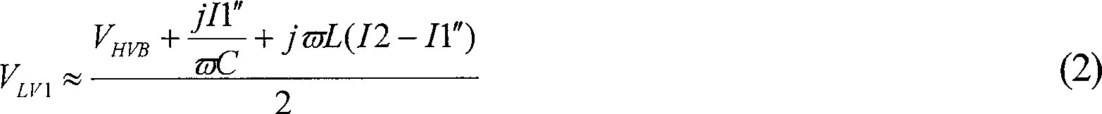
其中VHVB被定义为在高压侧HVB的电压。保护电路810A发送感测的电压改变控制器160,其依次立即采取动作防止由短路情况引起的破坏。如果高端电压HV1至HV4中的其中一个被短路到相应的低端电压,例如,HV1被短路到LV1,正常电流I1将明显地增加到电流I1″′,低端电压VLV1将相应地发生变化。低端电压VLV1通过等式(3)给出。where V HVB is defined as the voltage at the high side HVB. The

再一次的,保护电路810A发送感测电压变化到控制器160,其依次立即采取动作防止由短路情况导致的破坏。以类似的方式,保护电路810A可以检测到其它CCFL发生的短路情况。Again, the
本领域技术人员将认识到保护电路810A可以被扩展到如图8B示出的电路810B,其被用于保护如图4中所示的电路结构400免遭断开的灯或者短路情况。图4中的CCFL的低压侧VL1至LVN分别连接到电压感测电路810-1至810-N。基于由电压感测电路810-1至810-N感测的低端电压,在节点873上产生电压反馈信号VSEN,然后被馈送给图4中的控制器160。Those skilled in the art will recognize that the
本领域技术人员认识到与传统的保护电路相比,其中描述的保护电路由成本有竞争性的元件组成,同时元件数量被大大的减少。因此,可以获得节省的成本和尺寸。另外,其中描述的保护电路连接到CCFL的低压侧,从而可以不必在击穿或其它潜在的危害上付出额外的注意。另外,实现保护电路并不限于图4和6中的电路。实际上,本领域技术人员将承认其中描述的保护电路可以被应用到各种不同的背光电路结构,其中至少一个均衡扼流圈被连接到背光灯的低压侧。Those skilled in the art recognize that the protection circuit described therein is composed of cost-competitive components while the number of components is greatly reduced compared to conventional protection circuits. Thus, cost and size savings can be obtained. In addition, the protection circuit described therein is connected to the low voltage side of the CCFL, so that no extra care must be taken with regard to breakdown or other potential hazards. In addition, implementing the protection circuit is not limited to the circuits in FIGS. 4 and 6 . Indeed, those skilled in the art will recognize that the protection circuit described therein can be applied to various backlight circuit configurations in which at least one equalizing choke is connected to the low voltage side of the backlight.
图9示出了根据本发明另一实施例的具有多个CCFL的电路结构900的示意图。与图8A中的电路相比,电路900进一步包括由电流感测电阻901组成的电流感测电路910。如图9中所示,电流感测电阻901连接在CCFL 348和均衡扼流圈350的第二绕组354之间。电流感测电阻901和第二绕组354的连接节点进一步被连接到地。在电流感测电阻901和CCFL 348之间的连接节点上,获得电流反馈信号ISEN并被馈送给控制器160。为了响应电流反馈信号ISEN,控制器160可以调节灯电流,因此调节灯的亮度。因此,可以获得对灯的亮度的紧密控制。另外,应当注意由于电流感测电阻901的影响图8A中的电压感测电路868被删去,低端电压LV4被下拉到一低压并且再也不会指示例如断开的或者断路的灯的情况或者短路的异常情况。FIG. 9 shows a schematic diagram of a
实际上,指示流经CCFLs 342和348的电流的电流感测电压跨过电流感测电阻901形成,并且作为电流反馈信号ISEN被输入到控制器160。为了响应电流反馈信号ISEN,控制器160调节流经CCFL的电流从而调节CCFL的亮度。In effect, a current sense voltage indicative of the current flowing through
本领域技术人员将认识到电流感测电路910没有必要放置在CCFL 348和第二绕组354之间。有其它可能的结构,例如,电流感测电路910置于CCFL 342和第二绕组354之间。另外,电流感测电路910可以以相同的方法被应用到图4中具有多个CCFL的电路结构中。Those skilled in the art will recognize that it is not necessary for the
图10示出了根据本发明的另一实施例的具有多个CCFL的电路1000的示意图。与图4中的电路相比,电流感测电路1110连接在均衡扼流圈410-1的第二绕组403和均衡扼流圈410-2的第一绕组405之间。电流感测电路1110由第一二极管D1,第二二极管D2,一电流感测电阻Rs和电容器Cs组成。第一二极管D1的阳极连接到第二绕组403的终端3上,第一二极管D1的阴极连接到第一绕组405的终端2。第二二极管D2的阳极连接到第一绕组405的终端2从而第二二极管D2相对于第一二极管D1被反偏置。第二二极管D2的阴极通过电流感测电阻Rs连接到第二绕组403的终端3。电流感测电阻Rs进一步与电容器Cs并联。另外,第二绕组403的终端3被连接到地。在第二二极管D2和电流感测电阻Rs的连接节点1101,产生了电流反馈信号ISEN并且被馈送给控制器160。FIG. 10 shows a schematic diagram of a
实际上,指示流经CCFL 420-3和420-4的电流的电流感测电压跨过电流感测电阻Rs和电容器Cs生成,并且被作为电流反馈信号ISEN被输入到控制器160。为了响应电流反馈信号ISEN,控制器160调节流经CCFL的电流从而调节CCFL的亮度。In practice, a current sense voltage indicative of the current flowing through the CCFLs 420-3 and 420-4 is generated across the current sense resistor Rs and capacitor Cs, and is input to the
本领域技术人员将认识到不必一定将电流感测电路1110连接在均衡扼流圈410-1和410-2之间。相反,电流感测电路1110可以位于从410-1至410-(N/2-1)之间的两个任意相邻的均衡扼流圈之间。另外,可以包括图8B中的保护电路810B从而保护电路1000免遭断开的或者断路的灯的情况或者短路的情况。Those skilled in the art will recognize that it is not necessary to connect the
在操作中,电路结构可以包括一逆变器拓扑,多个负载,例如CCFL,连接到逆变器拓扑用于提供LCD面板的照明,连接到多个负载的用于平衡电灯电流的至少一个均衡扼流圈的电流平衡电路。多个负载中的至少两个负载通过至少一个均衡扼流圈串联。多个负载中的至少四个负载被连接到至少一个负载中的其中一个用于实现至少四个负载的电流均衡。至少一个均衡扼流圈连续的互相连接用以实现多个负载的电流平衡。In operation, the circuit configuration may include an inverter topology, a plurality of loads, such as CCFLs, connected to the inverter topology for providing illumination of the LCD panel, at least one equalizer connected to the plurality of loads for balancing lamp current Choke current balance circuit. At least two of the plurality of loads are connected in series through at least one balancing choke. At least four of the plurality of loads are connected to one of the at least one load for current balancing of the at least four loads. At least one equalizing choke is connected continuously to each other for current balancing of a plurality of loads.
另外,电路结构可以包括连接到多个负载的低压侧的保护电路。保护电路能够保护电路结构免遭断开的或者断路的灯的情况或者短路情况。而且,电路结构可以包括用于紧密控制电流亮度的电流感测电路。In addition, the circuit configuration may include a protection circuit connected to the low voltage side of the plurality of loads. The protection circuit is able to protect the circuit arrangement from a disconnected or disconnected lamp situation or a short circuit situation. Furthermore, the circuit configuration may include current sensing circuitry for tight control of current brightness.
本领域技术人员知道其中公开的电路结构可以被应用到包括Royer,全桥,半桥,推挽式,以及D级的各种不同的逆变器拓扑中。另外,控制器可以采取不同的变暗控制方法,包括模拟控制,脉冲调制(PWM)控制以及混合控制。本领域技术人员将认识到所有这些改变都在权利要求的范围之内。Those skilled in the art know that the circuit structure disclosed therein can be applied to various inverter topologies including Royer, full-bridge, half-bridge, push-pull, and Class-D. In addition, the controller can adopt different dimming control methods, including analog control, pulse modulation (PWM) control and hybrid control. Those skilled in the art will recognize that all such modifications are within the scope of the claims.
其中使用的术语和表达作为描述被应用但不受限制,使用这种术语和表达并不意图排除示出的和描述的等效的特征(或者其中的部分),应当认识到各种不同的改变在权利要求的可能的范围内。其它改变,变化以及替代也都是可能的,因此,权利要求试图覆盖所有这样的等效。The terms and expressions used therein are used as descriptions but not limitations. The use of such terms and expressions is not intended to exclude equivalent features (or parts thereof) shown and described, and various changes are recognized. within the scope of the claims. Other changes, variations, and substitutions are also possible, and the claims therefore attempt to cover all such equivalents.
Claims (19)
Applications Claiming Priority (3)
| Application Number | Priority Date | Filing Date | Title |
|---|---|---|---|
| US84578306P | 2006-09-18 | 2006-09-18 | |
| US60/845,783 | 2006-09-18 | ||
| US11/600,615 | 2006-11-15 |
Publications (2)
| Publication Number | Publication Date |
|---|---|
| CN101149501A CN101149501A (en) | 2008-03-26 |
| CN100504527C true CN100504527C (en) | 2009-06-24 |
Family
ID=39250099
Family Applications (1)
| Application Number | Title | Priority Date | Filing Date |
|---|---|---|---|
| CNB2007101546323A Expired - Fee Related CN100504527C (en) | 2006-09-18 | 2007-09-17 | Circuit structure for LCD backlight |
Country Status (1)
| Country | Link |
|---|---|
| CN (1) | CN100504527C (en) |
Families Citing this family (4)
| Publication number | Priority date | Publication date | Assignee | Title |
|---|---|---|---|---|
| KR101058684B1 (en) * | 2009-04-02 | 2011-08-22 | 삼성전기주식회사 | Lamp driving circuit |
| CN102186296A (en) * | 2011-05-20 | 2011-09-14 | 台达能源技术(上海)有限公司 | Current balancing circuit |
| CN103037554B (en) * | 2012-12-24 | 2015-12-09 | 泓芯泰业科技(北京)有限公司 | A kind of efficient cold light disc driving device |
| CN113194569A (en) * | 2021-04-09 | 2021-07-30 | 深圳市立创普电源技术有限公司 | Multi-path constant-current driving circuit and driving power supply |
-
2007
- 2007-09-17 CN CNB2007101546323A patent/CN100504527C/en not_active Expired - Fee Related
Also Published As
| Publication number | Publication date |
|---|---|
| CN101149501A (en) | 2008-03-26 |
Similar Documents
| Publication | Publication Date | Title |
|---|---|---|
| CN1887034B (en) | A current sharing scheme and device for multiple CCF lamp operation | |
| US7061183B1 (en) | Zigzag topology for balancing current among paralleled gas discharge lamps | |
| EP1581030B1 (en) | Parallel lighting system for surface light source discharge lamps | |
| TW200822035A (en) | A circuit structure for LCD backlight | |
| US7173382B2 (en) | Nested balancing topology for balancing current among multiple lamps | |
| US8120262B2 (en) | Driving circuit for multi-lamps | |
| JP2007018997A (en) | Equalizing of discharge lamp current in circuit | |
| CN100504527C (en) | Circuit structure for LCD backlight | |
| US20060244395A1 (en) | Electronic ballast having missing lamp detection | |
| US8247982B2 (en) | Method of driving a light source, light source assembly for performing the method, and liquid crystal display apparatus having the same | |
| CN101409972B (en) | For multiple cold cathode fluorescence lamps and/or the drive system of external-electrode fluorescent lamp and method | |
| US7446485B2 (en) | Multi-lamp driving system | |
| CN100591186C (en) | Method and protective device for driving discharge lamp in large panel application | |
| CN101317324B (en) | Power supply device, light emitting device and electronic equipment using the same | |
| US7408306B2 (en) | Lamp lighting circuit and device, and lamp lighting apparatus and device | |
| US7205726B2 (en) | Discharge lamp drive apparatus and liquid crystal display apparatus | |
| CN101115340B (en) | Inverter circuit | |
| US7224129B2 (en) | Discharge lamp drive apparatus and liquid crystal display apparatus | |
| HK1115643B (en) | A circuit structure for lcd backlight | |
| US7579789B2 (en) | Device for driving light sources | |
| JP4579800B2 (en) | Discharge lamp drive control circuit | |
| US7411356B2 (en) | Power supply for multiple discharge lamps and the current balance device thereof | |
| CN100346670C (en) | Voltage supply circuit of multiple lamp tubes | |
| CN1737651A (en) | Lamp drive circuit | |
| US20090289556A1 (en) | Discharge lamp lighting apparatus for lighting multiple discharge lamps |
Legal Events
| Date | Code | Title | Description |
|---|---|---|---|
| C06 | Publication | ||
| PB01 | Publication | ||
| C10 | Entry into substantive examination | ||
| SE01 | Entry into force of request for substantive examination | ||
| REG | Reference to a national code |
Ref country code: HK Ref legal event code: DE Ref document number: 1115643 Country of ref document: HK |
|
| C14 | Grant of patent or utility model | ||
| GR01 | Patent grant | ||
| REG | Reference to a national code |
Ref country code: HK Ref legal event code: GR Ref document number: 1115643 Country of ref document: HK |
|
| ASS | Succession or assignment of patent right |
Owner name: O2 TECH. INTERNATIONAL LTD. Free format text: FORMER OWNER: O2 MICRO INC Effective date: 20101122 |
|
| C41 | Transfer of patent application or patent right or utility model | ||
| COR | Change of bibliographic data |
Free format text: CORRECT: ADDRESS; FROM: CALIFORNIA, AMERICA TO: ENGLISH CAYMAN ISLANDS, ENGLAND |
|
| TR01 | Transfer of patent right |
Effective date of registration: 20101122 Address after: British Cayman Islands Patentee after: O2 Tech. International Ltd. Address before: American California Patentee before: O2 Micro Inc |
|
| CF01 | Termination of patent right due to non-payment of annual fee |
Granted publication date: 20090624 Termination date: 20140917 |
|
| EXPY | Termination of patent right or utility model |