CN100500656C - Metal coordination compound and electroluminescence device - Google Patents
Metal coordination compound and electroluminescence device Download PDFInfo
- Publication number
- CN100500656C CN100500656C CNB028087011A CN02808701A CN100500656C CN 100500656 C CN100500656 C CN 100500656C CN B028087011 A CNB028087011 A CN B028087011A CN 02808701 A CN02808701 A CN 02808701A CN 100500656 C CN100500656 C CN 100500656C
- Authority
- CN
- China
- Prior art keywords
- light
- layer
- emitting
- metal
- organic
- Prior art date
- Legal status (The legal status is an assumption and is not a legal conclusion. Google has not performed a legal analysis and makes no representation as to the accuracy of the status listed.)
- Expired - Fee Related
Links
Images


Classifications
-
- C—CHEMISTRY; METALLURGY
- C07—ORGANIC CHEMISTRY
- C07F—ACYCLIC, CARBOCYCLIC OR HETEROCYCLIC COMPOUNDS CONTAINING ELEMENTS OTHER THAN CARBON, HYDROGEN, HALOGEN, OXYGEN, NITROGEN, SULFUR, SELENIUM OR TELLURIUM
- C07F15/00—Compounds containing elements of Groups 8, 9, 10 or 18 of the Periodic Table
-
- C—CHEMISTRY; METALLURGY
- C07—ORGANIC CHEMISTRY
- C07D—HETEROCYCLIC COMPOUNDS
- C07D221/00—Heterocyclic compounds containing six-membered rings having one nitrogen atom as the only ring hetero atom, not provided for by groups C07D211/00 - C07D219/00
- C07D221/02—Heterocyclic compounds containing six-membered rings having one nitrogen atom as the only ring hetero atom, not provided for by groups C07D211/00 - C07D219/00 condensed with carbocyclic rings or ring systems
- C07D221/04—Ortho- or peri-condensed ring systems
- C07D221/06—Ring systems of three rings
- C07D221/16—Ring systems of three rings containing carbocyclic rings other than six-membered
-
- C—CHEMISTRY; METALLURGY
- C07—ORGANIC CHEMISTRY
- C07D—HETEROCYCLIC COMPOUNDS
- C07D221/00—Heterocyclic compounds containing six-membered rings having one nitrogen atom as the only ring hetero atom, not provided for by groups C07D211/00 - C07D219/00
- C07D221/02—Heterocyclic compounds containing six-membered rings having one nitrogen atom as the only ring hetero atom, not provided for by groups C07D211/00 - C07D219/00 condensed with carbocyclic rings or ring systems
- C07D221/04—Ortho- or peri-condensed ring systems
- C07D221/06—Ring systems of three rings
- C07D221/10—Aza-phenanthrenes
-
- C—CHEMISTRY; METALLURGY
- C09—DYES; PAINTS; POLISHES; NATURAL RESINS; ADHESIVES; COMPOSITIONS NOT OTHERWISE PROVIDED FOR; APPLICATIONS OF MATERIALS NOT OTHERWISE PROVIDED FOR
- C09K—MATERIALS FOR MISCELLANEOUS APPLICATIONS, NOT PROVIDED FOR ELSEWHERE
- C09K11/00—Luminescent, e.g. electroluminescent, chemiluminescent materials
- C09K11/06—Luminescent, e.g. electroluminescent, chemiluminescent materials containing organic luminescent materials
-
- H—ELECTRICITY
- H05—ELECTRIC TECHNIQUES NOT OTHERWISE PROVIDED FOR
- H05B—ELECTRIC HEATING; ELECTRIC LIGHT SOURCES NOT OTHERWISE PROVIDED FOR; CIRCUIT ARRANGEMENTS FOR ELECTRIC LIGHT SOURCES, IN GENERAL
- H05B33/00—Electroluminescent light sources
- H05B33/12—Light sources with substantially two-dimensional radiating surfaces
- H05B33/14—Light sources with substantially two-dimensional radiating surfaces characterised by the chemical or physical composition or the arrangement of the electroluminescent material, or by the simultaneous addition of the electroluminescent material in or onto the light source
-
- H—ELECTRICITY
- H10—SEMICONDUCTOR DEVICES; ELECTRIC SOLID-STATE DEVICES NOT OTHERWISE PROVIDED FOR
- H10K—ORGANIC ELECTRIC SOLID-STATE DEVICES
- H10K85/00—Organic materials used in the body or electrodes of devices covered by this subclass
- H10K85/30—Coordination compounds
- H10K85/341—Transition metal complexes, e.g. Ru(II)polypyridine complexes
- H10K85/342—Transition metal complexes, e.g. Ru(II)polypyridine complexes comprising iridium
-
- C—CHEMISTRY; METALLURGY
- C09—DYES; PAINTS; POLISHES; NATURAL RESINS; ADHESIVES; COMPOSITIONS NOT OTHERWISE PROVIDED FOR; APPLICATIONS OF MATERIALS NOT OTHERWISE PROVIDED FOR
- C09K—MATERIALS FOR MISCELLANEOUS APPLICATIONS, NOT PROVIDED FOR ELSEWHERE
- C09K2211/00—Chemical nature of organic luminescent or tenebrescent compounds
- C09K2211/10—Non-macromolecular compounds
- C09K2211/1003—Carbocyclic compounds
- C09K2211/1007—Non-condensed systems
-
- C—CHEMISTRY; METALLURGY
- C09—DYES; PAINTS; POLISHES; NATURAL RESINS; ADHESIVES; COMPOSITIONS NOT OTHERWISE PROVIDED FOR; APPLICATIONS OF MATERIALS NOT OTHERWISE PROVIDED FOR
- C09K—MATERIALS FOR MISCELLANEOUS APPLICATIONS, NOT PROVIDED FOR ELSEWHERE
- C09K2211/00—Chemical nature of organic luminescent or tenebrescent compounds
- C09K2211/10—Non-macromolecular compounds
- C09K2211/1003—Carbocyclic compounds
- C09K2211/1011—Condensed systems
-
- C—CHEMISTRY; METALLURGY
- C09—DYES; PAINTS; POLISHES; NATURAL RESINS; ADHESIVES; COMPOSITIONS NOT OTHERWISE PROVIDED FOR; APPLICATIONS OF MATERIALS NOT OTHERWISE PROVIDED FOR
- C09K—MATERIALS FOR MISCELLANEOUS APPLICATIONS, NOT PROVIDED FOR ELSEWHERE
- C09K2211/00—Chemical nature of organic luminescent or tenebrescent compounds
- C09K2211/10—Non-macromolecular compounds
- C09K2211/1003—Carbocyclic compounds
- C09K2211/1014—Carbocyclic compounds bridged by heteroatoms, e.g. N, P, Si or B
-
- C—CHEMISTRY; METALLURGY
- C09—DYES; PAINTS; POLISHES; NATURAL RESINS; ADHESIVES; COMPOSITIONS NOT OTHERWISE PROVIDED FOR; APPLICATIONS OF MATERIALS NOT OTHERWISE PROVIDED FOR
- C09K—MATERIALS FOR MISCELLANEOUS APPLICATIONS, NOT PROVIDED FOR ELSEWHERE
- C09K2211/00—Chemical nature of organic luminescent or tenebrescent compounds
- C09K2211/10—Non-macromolecular compounds
- C09K2211/1018—Heterocyclic compounds
- C09K2211/1025—Heterocyclic compounds characterised by ligands
- C09K2211/1029—Heterocyclic compounds characterised by ligands containing one nitrogen atom as the heteroatom
-
- C—CHEMISTRY; METALLURGY
- C09—DYES; PAINTS; POLISHES; NATURAL RESINS; ADHESIVES; COMPOSITIONS NOT OTHERWISE PROVIDED FOR; APPLICATIONS OF MATERIALS NOT OTHERWISE PROVIDED FOR
- C09K—MATERIALS FOR MISCELLANEOUS APPLICATIONS, NOT PROVIDED FOR ELSEWHERE
- C09K2211/00—Chemical nature of organic luminescent or tenebrescent compounds
- C09K2211/10—Non-macromolecular compounds
- C09K2211/1018—Heterocyclic compounds
- C09K2211/1025—Heterocyclic compounds characterised by ligands
- C09K2211/1044—Heterocyclic compounds characterised by ligands containing two nitrogen atoms as heteroatoms
-
- C—CHEMISTRY; METALLURGY
- C09—DYES; PAINTS; POLISHES; NATURAL RESINS; ADHESIVES; COMPOSITIONS NOT OTHERWISE PROVIDED FOR; APPLICATIONS OF MATERIALS NOT OTHERWISE PROVIDED FOR
- C09K—MATERIALS FOR MISCELLANEOUS APPLICATIONS, NOT PROVIDED FOR ELSEWHERE
- C09K2211/00—Chemical nature of organic luminescent or tenebrescent compounds
- C09K2211/10—Non-macromolecular compounds
- C09K2211/1018—Heterocyclic compounds
- C09K2211/1025—Heterocyclic compounds characterised by ligands
- C09K2211/1088—Heterocyclic compounds characterised by ligands containing oxygen as the only heteroatom
-
- C—CHEMISTRY; METALLURGY
- C09—DYES; PAINTS; POLISHES; NATURAL RESINS; ADHESIVES; COMPOSITIONS NOT OTHERWISE PROVIDED FOR; APPLICATIONS OF MATERIALS NOT OTHERWISE PROVIDED FOR
- C09K—MATERIALS FOR MISCELLANEOUS APPLICATIONS, NOT PROVIDED FOR ELSEWHERE
- C09K2211/00—Chemical nature of organic luminescent or tenebrescent compounds
- C09K2211/10—Non-macromolecular compounds
- C09K2211/1018—Heterocyclic compounds
- C09K2211/1025—Heterocyclic compounds characterised by ligands
- C09K2211/1092—Heterocyclic compounds characterised by ligands containing sulfur as the only heteroatom
-
- C—CHEMISTRY; METALLURGY
- C09—DYES; PAINTS; POLISHES; NATURAL RESINS; ADHESIVES; COMPOSITIONS NOT OTHERWISE PROVIDED FOR; APPLICATIONS OF MATERIALS NOT OTHERWISE PROVIDED FOR
- C09K—MATERIALS FOR MISCELLANEOUS APPLICATIONS, NOT PROVIDED FOR ELSEWHERE
- C09K2211/00—Chemical nature of organic luminescent or tenebrescent compounds
- C09K2211/18—Metal complexes
- C09K2211/181—Metal complexes of the alkali metals and alkaline earth metals
-
- C—CHEMISTRY; METALLURGY
- C09—DYES; PAINTS; POLISHES; NATURAL RESINS; ADHESIVES; COMPOSITIONS NOT OTHERWISE PROVIDED FOR; APPLICATIONS OF MATERIALS NOT OTHERWISE PROVIDED FOR
- C09K—MATERIALS FOR MISCELLANEOUS APPLICATIONS, NOT PROVIDED FOR ELSEWHERE
- C09K2211/00—Chemical nature of organic luminescent or tenebrescent compounds
- C09K2211/18—Metal complexes
- C09K2211/185—Metal complexes of the platinum group, i.e. Os, Ir, Pt, Ru, Rh or Pd
-
- H—ELECTRICITY
- H10—SEMICONDUCTOR DEVICES; ELECTRIC SOLID-STATE DEVICES NOT OTHERWISE PROVIDED FOR
- H10K—ORGANIC ELECTRIC SOLID-STATE DEVICES
- H10K2101/00—Properties of the organic materials covered by group H10K85/00
- H10K2101/10—Triplet emission
-
- H—ELECTRICITY
- H10—SEMICONDUCTOR DEVICES; ELECTRIC SOLID-STATE DEVICES NOT OTHERWISE PROVIDED FOR
- H10K—ORGANIC ELECTRIC SOLID-STATE DEVICES
- H10K50/00—Organic light-emitting devices
- H10K50/10—OLEDs or polymer light-emitting diodes [PLED]
- H10K50/11—OLEDs or polymer light-emitting diodes [PLED] characterised by the electroluminescent [EL] layers
-
- H—ELECTRICITY
- H10—SEMICONDUCTOR DEVICES; ELECTRIC SOLID-STATE DEVICES NOT OTHERWISE PROVIDED FOR
- H10K—ORGANIC ELECTRIC SOLID-STATE DEVICES
- H10K59/00—Integrated devices, or assemblies of multiple devices, comprising at least one organic light-emitting element covered by group H10K50/00
- H10K59/10—OLED displays
- H10K59/12—Active-matrix OLED [AMOLED] displays
-
- H—ELECTRICITY
- H10—SEMICONDUCTOR DEVICES; ELECTRIC SOLID-STATE DEVICES NOT OTHERWISE PROVIDED FOR
- H10K—ORGANIC ELECTRIC SOLID-STATE DEVICES
- H10K85/00—Organic materials used in the body or electrodes of devices covered by this subclass
- H10K85/30—Coordination compounds
- H10K85/321—Metal complexes comprising a group IIIA element, e.g. Tris (8-hydroxyquinoline) gallium [Gaq3]
- H10K85/324—Metal complexes comprising a group IIIA element, e.g. Tris (8-hydroxyquinoline) gallium [Gaq3] comprising aluminium, e.g. Alq3
-
- H—ELECTRICITY
- H10—SEMICONDUCTOR DEVICES; ELECTRIC SOLID-STATE DEVICES NOT OTHERWISE PROVIDED FOR
- H10K—ORGANIC ELECTRIC SOLID-STATE DEVICES
- H10K85/00—Organic materials used in the body or electrodes of devices covered by this subclass
- H10K85/30—Coordination compounds
- H10K85/341—Transition metal complexes, e.g. Ru(II)polypyridine complexes
- H10K85/346—Transition metal complexes, e.g. Ru(II)polypyridine complexes comprising platinum
-
- H—ELECTRICITY
- H10—SEMICONDUCTOR DEVICES; ELECTRIC SOLID-STATE DEVICES NOT OTHERWISE PROVIDED FOR
- H10K—ORGANIC ELECTRIC SOLID-STATE DEVICES
- H10K85/00—Organic materials used in the body or electrodes of devices covered by this subclass
- H10K85/60—Organic compounds having low molecular weight
- H10K85/631—Amine compounds having at least two aryl rest on at least one amine-nitrogen atom, e.g. triphenylamine
-
- H—ELECTRICITY
- H10—SEMICONDUCTOR DEVICES; ELECTRIC SOLID-STATE DEVICES NOT OTHERWISE PROVIDED FOR
- H10K—ORGANIC ELECTRIC SOLID-STATE DEVICES
- H10K85/00—Organic materials used in the body or electrodes of devices covered by this subclass
- H10K85/60—Organic compounds having low molecular weight
- H10K85/649—Aromatic compounds comprising a hetero atom
-
- Y—GENERAL TAGGING OF NEW TECHNOLOGICAL DEVELOPMENTS; GENERAL TAGGING OF CROSS-SECTIONAL TECHNOLOGIES SPANNING OVER SEVERAL SECTIONS OF THE IPC; TECHNICAL SUBJECTS COVERED BY FORMER USPC CROSS-REFERENCE ART COLLECTIONS [XRACs] AND DIGESTS
- Y10—TECHNICAL SUBJECTS COVERED BY FORMER USPC
- Y10S—TECHNICAL SUBJECTS COVERED BY FORMER USPC CROSS-REFERENCE ART COLLECTIONS [XRACs] AND DIGESTS
- Y10S428/00—Stock material or miscellaneous articles
- Y10S428/917—Electroluminescent
Landscapes
- Chemical & Material Sciences (AREA)
- Organic Chemistry (AREA)
- Engineering & Computer Science (AREA)
- Materials Engineering (AREA)
- Crystallography & Structural Chemistry (AREA)
- Inorganic Chemistry (AREA)
- Electroluminescent Light Sources (AREA)
- Plural Heterocyclic Compounds (AREA)
- Organic Low-Molecular-Weight Compounds And Preparation Thereof (AREA)
- Other In-Based Heterocyclic Compounds (AREA)
- Devices For Indicating Variable Information By Combining Individual Elements (AREA)
Abstract
Description
技术领域 technical field
本发明涉及利用有机化合物的电致发光装置,更特别地涉及用金属配位化合物作发光材料的有机电致发光装置(下文中称为“有机EL装置”)。The present invention relates to electroluminescent devices using organic compounds, and more particularly to organic electroluminescent devices (hereinafter referred to as "organic EL devices") using metal complex compounds as light-emitting materials.
背景技术 Background technique
有机EL装置作为高速响应性和高效发光装置的应用研究一直在积极进行。其基本结构示于图1(a)和(b)中(例如Macromol Symp.125,1-48(1977))。Applied research on organic EL devices as high-speed responsiveness and high-efficiency light emitting devices has been actively conducted. Its basic structure is shown in Fig. 1(a) and (b) (eg Macromol Symp. 125, 1-48 (1977)).
如图1中所示,有机EL装置一般有这样的结构,包括在透明基板15之上的透明电极14、金属电极11、和置于其间的多个有机薄膜层。As shown in FIG. 1, an organic EL device generally has a structure including a transparent electrode 14 on a transparent substrate 15, a metal electrode 11, and a plurality of organic thin film layers interposed therebetween.
图1(a)的装置中,所述有机层包括发光层12和空穴迁移层13。所述透明电极14使用有大功函的ITO等以提供从透明电极14至空穴迁移层13的良好的空穴注入特性。所述金属电极11使用小功函的金属如铝、镁或这些金属的合金以提供良好的电子注入特性。这些电极的厚度为50-200nm。In the device of FIG. 1( a ), the organic layers include a light emitting layer 12 and a hole transport layer 13 . The transparent electrode 14 uses ITO or the like having a large work function to provide good hole injection properties from the transparent electrode 14 to the hole transport layer 13 . The metal electrode 11 uses a metal with a small work function such as aluminum, magnesium or an alloy of these metals to provide good electron injection properties. The thickness of these electrodes is 50-200 nm.
所述发光层12使用有电子迁移特性和发光特性的铝-羟基喹啉配合物(其典型实例是下文所示Alq3)等。所述空穴迁移层使用有给电子特性的联苯二胺衍生物(其典型实例是下文所示α-NPD)等。The light-emitting layer 12 uses an aluminum-quinolinol complex having electron transport properties and light-emitting properties (a typical example of which is Alq3 shown below) or the like. The hole transport layer uses a biphenylenediamine derivative having electron-donating properties (a typical example of which is α-NPD shown below) or the like.
上述结构的装置有整流特性,在作为阴极的金属电极11和作为阳极的透明电极14之间施加电场时,由金属电极11向发光层12注入电子并由透明电极15注入空穴。注入的空穴和电子在发光层12内重组形成激发子而产生激发光。此时,空穴迁移层13起电子阻挡层的作用以提高发光层12和空穴迁移层13间界面处的重组效率,从而提高发光效率。The device with the above structure has rectification characteristics. When an electric field is applied between the metal electrode 11 as the cathode and the transparent electrode 14 as the anode, electrons are injected from the metal electrode 11 to the light-emitting layer 12 and holes are injected from the transparent electrode 15 . The injected holes and electrons recombine in the light-emitting layer 12 to form excitons to generate excitation light. At this time, the hole transport layer 13 functions as an electron blocking layer to increase the recombination efficiency at the interface between the light emitting layer 12 and the hole transport layer 13, thereby increasing the luminous efficiency.
而在图1(b)的结构中,电子迁移层16置于金属电极11和发光层12之间。使发光与电子和空穴迁移分离提供更有效的载流子阻挡结构,可实现有效发光。所述电子迁移层16使用电子迁移材料如含氧二唑(oxidiazole)衍生物。However, in the structure of FIG. 1( b ), the electron transport layer 16 is placed between the metal electrode 11 and the light emitting layer 12 . Separating luminescence from electron and hole transport provides a more efficient carrier blocking structure that enables efficient luminescence. The electron transport layer 16 uses an electron transport material such as oxidiazole derivatives.
迄今已知的有机EL装置中所用发光方法包括荧光和磷光。在荧光发光装置中,从单重激子状态跃迁至基态时产生荧光。另一方面,在磷光发光装置中,利用从三重激子状态至基态的跃迁。Light-emitting methods used in hitherto known organic EL devices include fluorescence and phosphorescence. In fluorescent light-emitting devices, fluorescence is generated upon transition from a singlet excitonic state to a ground state. On the other hand, in a phosphorescent light-emitting device, a transition from a triplet exciton state to a ground state is utilized.
近年来,一直在研究发光率比利用荧光的装置更高的利用磷光的装置。In recent years, devices using phosphorescence having a higher luminous efficiency than devices using fluorescence have been studied.
代表性的公开文献可包括:Representative publications may include:
论文1:电致磷光装置中改进的能量转移(D.F.O’Brien,etal.,Applied Physics Letters,Vol.74,No.3,p.422(1999));和Paper 1: Improved Energy Transfer in Electrophosphorescent Devices (D.F.O'Brien, et al., Applied Physics Letters, Vol.74, No.3, p.422 (1999)); and
论文2:基于电致磷光的极高效的绿色有机发光装置(M.A.Baldo,et al.,Applied Physics Letters,Vol.75,No.1,p.4(1999))。Paper 2: An extremely efficient green organic light-emitting device based on electrophosphorescence (M.A. Baldo, et al., Applied Physics Letters, Vol.75, No.1, p.4(1999)).
这些论文中,主要使用包括图1(c)所示4有机层装置的结构,包括(从阳极侧)空穴迁移层13、发光层12、防止激发子扩散层17和电子迁移层16。其中所用材料包括载流子迁移材料和磷光材料,下面示出其中的缩写。In these papers, a structure comprising a 4-organic layer device as shown in FIG. 1(c), including (from the anode side) a hole transport layer 13, an emission layer 12, an exciton diffusion prevention layer 17, and an electron transport layer 16, is mainly used. The materials used therein include carrier transport materials and phosphorescent materials, the abbreviations of which are shown below.
Alq3:铝-羟基喹啉配合物Alq3: aluminum-hydroxyquinoline complex
α-NPD:N4,N4’-二-萘-1-基-N4,N4’-二苯基-联苯-4,4’-二胺α-NPD: N4,N4'-di-naphthalen-1-yl-N4,N4'-diphenyl-biphenyl-4,4'-diamine
CBP:4,4’-N,N’-二咔唑-联苯CBP: 4,4'-N,N'-dicarbazole-biphenyl
BCP:2,9-二甲基-4,7-二苯基-1,10-菲咯啉BCP: 2,9-Dimethyl-4,7-diphenyl-1,10-phenanthroline
PtOEP:铂-八乙基卟啉配合物PtOEP: platinum-octaethylporphyrin complex
Ir(ppy)3:铱-苯基嘧啶配合物Ir(ppy) 3 : Iridium-phenylpyrimidine complex
上述利用磷光的有机EL装置伴有发光衰退的问题,尤其是在供能状态下。发光衰退的原因尚不清楚,但此现象的原因可归因于三重激子的寿命比单重激子的寿命长至少三位数,从而使分子长时间处于高能状态导致与环境物质反应、生成激态复合物或激态分子、瞬间分子结构改变、环境物质结构改变等。The above-mentioned organic EL devices utilizing phosphorescence are accompanied by a problem of light emission fading, especially in an energized state. The reason for the decay of luminescence is not clear, but the reason for this phenomenon can be attributed to the fact that the lifetime of triplet excitons is at least three digits longer than that of singlet excitons, so that the molecule is in a high-energy state for a long time, causing reactions with environmental substances, generating Exciplexes or excimer molecules, instantaneous molecular structure changes, environmental material structure changes, etc.
总之,如上所述,预计磷光发光装置提供较高的发光效率,但该EL装置伴有在供能状态下发光衰退的问题。想要产生高效发光且有高稳定性的化合物作为磷光装置中所用发光材料。In conclusion, as described above, phosphorescent light-emitting devices are expected to provide high luminous efficiency, but the EL device is accompanied by a problem of light emission decay in an energized state. Compounds that emit light efficiently and have high stability are desired as light-emitting materials for use in phosphorescent devices.
发明内容 Contents of the invention
因此,本发明的目的是提供能产生高效发光并长时间保持高发光度(亮度)的稳定发光装置。作为新的发光材料,本发明提供一种特殊的金属配位化合物。Accordingly, an object of the present invention is to provide a stable light-emitting device capable of producing high-efficiency light emission and maintaining high luminosity (brightness) for a long period of time. As a new luminescent material, the invention provides a special metal coordination compound.
本发明所述金属配位化合物用下式(1)表示:The metal coordination compound of the present invention is represented by the following formula (1):
MLmL’n (1)ML m L' n (1)
其中M为Ir、Pt、Rh或Pd的金属原子;L和L’为相互不同的二齿配体;m为1、2或3;n为0、1或2,条件是m+n为2或3;部分结构MLm用以下所示式(2)表示,部分结构ML’n用以下所示式(3)、(4)或(5)表示:wherein M is a metal atom of Ir, Pt, Rh or Pd; L and L' are mutually different bidentate ligands; m is 1, 2 or 3; n is 0, 1 or 2, provided that m+n is 2 Or 3; the partial structure ML m is expressed by the following formula (2), and the partial structure ML' n is expressed by the following formula (3), (4) or (5):
其中N和C分别为氮和碳原子;A和A’分别为能有取代基并通过所述氮原子与金属原子M键合的环状基团;B、B’和B”分别为能有取代基并通过所述碳原子与金属原子M相连的环状基团;Wherein N and C are respectively nitrogen and carbon atoms; A and A' are respectively capable of having a substituent and are bonded to the metal atom M through the nitrogen atom; B, B' and B" are respectively capable of having A substituent and a cyclic group connected to the metal atom M through the carbon atom;
{其中所述取代基选自卤原子、氰基、硝基、三烷基甲硅烷基(其中所述烷基独立地为有1至8个碳原子的直链或支链烷基)、有1至20个碳原子的直链或支链烷基(其中所述烷基可包括一个或不相邻的两或多个可用-O-、-S-、-CO-、-CO-O-、-O-CO-、-CH=CH-或-C≡C-代替的亚甲基而且所述烷基可包括可用氟原子代替的氢原子)、或能有取代基的芳族环状基团(其中所述取代基为卤原子、氰基、硝基、或有1至20个碳原子的直链或支链烷基(其中所述烷基可包括一个或不相邻的两或多个可用-O-、-S-、-CO-、-CO-O-、-O-CO-、-CH=CH-或-C≡C-代替的亚甲基而且所述烷基可包括可用氟原子代替的氢原子)};{wherein said substituent is selected from halogen atom, cyano group, nitro group, trialkylsilyl group (wherein said alkyl group is independently a linear or branched chain alkyl group with 1 to 8 carbon atoms), 1 to 20 carbon atoms straight or branched chain alkyl (wherein said alkyl may include one or two or more non-adjacent -O-, -S-, -CO-, -CO-O- , -O-CO-, -CH=CH- or -C≡C-substituted methylene and the alkyl group may include a hydrogen atom that can be replaced by a fluorine atom), or an aromatic cyclic group that can have a substituent group (wherein the substituent is a halogen atom, cyano group, nitro group, or a linear or branched alkyl group with 1 to 20 carbon atoms (wherein the alkyl group may include one or non-adjacent two or more a methylene group which may be replaced by -O-, -S-, -CO-, -CO-O-, -O-CO-, -CH=CH- or -C≡C- and the alkyl group may include the available Hydrogen atoms replaced by fluorine atoms)};
A和B、A’和B’、及A”和B”分别通过共价键彼此键合;A和B、及A’和B’分别通过X和X’彼此键合;A and B, A' and B', and A" and B", respectively, are bound to each other by a covalent bond; A and B, and A' and B' are respectively bound to each other by X and X';
X和X’独立地为有2至10个碳原子的直链或支链亚烷基(其中所述亚烷基可包括一个或不相邻的两或多个可用-O-、-S-、-CO-、-CO-O-、-O-CO-、-CH=CH-或-C≡C-代替的亚甲基而且所述亚烷基可包括可用氟原子代替的氢原子);X and X' are independently linear or branched alkylene groups having 2 to 10 carbon atoms (wherein the alkylene group may include one or non-adjacent two or more available -O-, -S- , -CO-, -CO-O-, -O-CO-, -CH=CH- or -C≡C-substituted methylene and said alkylene may include hydrogen atoms that may be replaced by fluorine atoms);
E和G独立地为有1至20个碳原子的直链或支链烷基(其中所述烷基可包括任选地用氟原子代替的氢原子)、或能有取代基的芳族环状基团(其中所述取代基为卤原子、氰基、硝基、三烷基甲硅烷基(其中所述烷基独立地为有1至8个碳原子的直链或支链烷基)、或有1至20个碳原子的直链或支链烷基(其中所述烷基可包括一个或不相邻的两或多个可用-O-、-S-、-CO-、-CO-O-、-O-CO-、-CH=CH-或-C≡C-代替的亚甲基而且所述烷基可包括可用氟原子代替的氢原子))。E and G are independently a linear or branched alkyl group having 1 to 20 carbon atoms (wherein the alkyl group may include a hydrogen atom optionally substituted with a fluorine atom), or an aromatic ring capable of substituents Like group (wherein the substituent is halogen atom, cyano group, nitro group, trialkylsilyl group (wherein the alkyl group is independently a linear or branched chain alkyl group with 1 to 8 carbon atoms) , or a linear or branched alkyl group with 1 to 20 carbon atoms (wherein the alkyl group may include one or non-adjacent two or more available -O-, -S-, -CO-, -CO -O-, -O-CO-, -CH═CH- or -C≡C-substituted methylene and the alkyl group may include hydrogen atoms which may be replaced by fluorine atoms)).
本发明所述金属配位化合物可优选为其中式(1)中n为0;式(1)中部分结构ML’n为式(3)表示;式(1)中部分结构ML’n为式(4)表示;或式(1)中部分结构ML’n为式(5)表示的那些。The metal coordination compound of the present invention may preferably be wherein n in the formula (1) is 0; the partial structure ML'n in the formula (1) is represented by the formula (3); the partial structure ML'n in the formula (1) is the formula (4) represents; or the partial structure ML'n in formula (1) is those represented by formula (5).
此外,式(1)中,X可优选为有2至6个碳原子的直链或支链亚烷基(其中所述亚烷基可包括一个或不相邻的两或多个可用-O-、-S-、-CO-、-CO-O-、-O-CO-、-CH=CH-或-C≡C-代替的亚甲基而且所述亚烷基可包括可用氟原子代替的氢原子)。In addition, in formula (1), X may preferably be a linear or branched alkylene group having 2 to 6 carbon atoms (wherein the alkylene group may include one or non-adjacent two or more available -O -, -S-, -CO-, -CO-O-, -O-CO-, -CH═CH- or -C≡C-substituted methylene and the alkylene may include substituted fluorine atoms hydrogen atoms).
此外,所述金属配位化合物可优选包含Ir作为如上所述式(1)中的M。In addition, the metal coordination compound may preferably contain Ir as M in formula (1) as described above.
此外,本发明还提供一种电致发光装置,其中包含上述金属配位化合物的层夹在两个相对设置的电极之间,在所述电极之间施加电压产生激发光。In addition, the present invention also provides an electroluminescent device, wherein a layer containing the above-mentioned metal coordination compound is sandwiched between two opposite electrodes, and a voltage is applied between the electrodes to generate excitation light.
特别地,所述电致发光装置可优选为产生磷光的电致发光装置。In particular, the electroluminescent device may preferably be an electroluminescent device that generates phosphorescence.
附图简述Brief description of the drawings
图1说明本发明发光装置的实施方案,其中(a)为有两个有机层的装置结构,(b)为有三个有机层的装置结构,(c)为有四个有机层的装置结构。Figure 1 illustrates an embodiment of a light-emitting device of the present invention, wherein (a) is a device structure with two organic layers, (b) is a device structure with three organic layers, and (c) is a device structure with four organic layers.
图2示意地说明包括有机EL装置和驱动装置的面板结构的例子。FIG. 2 schematically illustrates an example of a panel structure including an organic EL device and a driving device.
图3说明使用TFTs(薄膜晶体管)的像素电路的例子。FIG. 3 illustrates an example of a pixel circuit using TFTs (Thin Film Transistors).
实施本发明的最佳方式Best Mode for Carrying Out the Invention
在发光层由载流子迁移主体材料和磷光客体材料形成的情况下,为改善所得有机EL装置的发光效率,要求中心发光材料本身提供较高的发光量子产量。此外,主体材料分子之间或主体材料分子与客体材料分子之间的有效能量转移也是重要因素。In the case where the light-emitting layer is formed of a carrier-transferring host material and a phosphorescent guest material, in order to improve the luminous efficiency of the resulting organic EL device, the central luminescent material itself is required to provide a higher luminescent quantum yield. In addition, efficient energy transfer between host material molecules or between host material molecules and guest material molecules is also an important factor.
此外,发光衰退的原因尚不清楚,但可推测至少与发光材料本身或因其周围分子结构所致环境变化有关。In addition, the cause of luminescence decay is not clear, but it can be speculated that it is at least related to the luminescent material itself or the environmental change caused by its surrounding molecular structure.
为此,本发明人进行了许多研究,发现了上述式(1)所示金属配位化合物,而且发现使用所述发光材料的有机EL装置能高效发光、长时间保持高亮度(发光度)、而且在供能状态的(发光)衰退较小。For this reason, the present inventor has carried out many researches, has found the metal coordination compound shown in above-mentioned formula (1), and finds that the organic EL device that uses described light-emitting material can emit light efficiently, keep high brightness (luminosity) for a long time, Also the (luminescence) decay in the energized state is smaller.
式(1)的金属配位化合物中,n可优选为0或1,更优选为0。此外,所述部分结构ML’n可优选为上述式(3)表示。In the metal coordination compound of formula (1), n may preferably be 0 or 1, more preferably 0. In addition, the partial structure ML'n may preferably be represented by the above formula (3).
此外,式(1)中,X可优选为有2至10个碳原子的直链或支链亚烷基(其中所述亚烷基可包括一个或不相邻的两或多个可用-O-、-S-、-CO-、-CO-O-、-O-CO-、-CH=CH-或-C≡C-代替的亚甲基而且所述亚烷基可包括可用氟原子代替的氢原子)。此外,式中M可优选为Ir或Rh,更优选为Ir。In addition, in formula (1), X may preferably be a linear or branched alkylene group having 2 to 10 carbon atoms (wherein the alkylene group may include one or non-adjacent two or more available -O -, -S-, -CO-, -CO-O-, -O-CO-, -CH═CH- or -C≡C-substituted methylene and the alkylene may include substituted fluorine atoms hydrogen atoms). In addition, M in the formula may preferably be Ir or Rh, more preferably Ir.
本发明所用金属配位化合物发射磷光,据信,其最低激发态为三重态中的MLCT*(金属至配体电荷转移)激发态或π-π*激发态,在从此态跃迁至基态时产生磷光。The metal coordination compounds used in the present invention emit phosphorescence, the lowest excited state of which is believed to be the MLCT* (metal-to-ligand charge transfer) excited state or the π-π* excited state in the triplet state, which occurs upon transition from this state to the ground state Phosphorescence.
<物理性能的测量方法><Measurement method of physical properties>
下面描述本发明中物理性能的测量方法。The measurement methods of the physical properties in the present invention are described below.
(1)磷光和荧光之间的判断方法(1) Judgment method between phosphorescence and fluorescence
根据是否被氧气减活化来鉴别磷光。使(试样)化合物溶于氯仿,充以氧气或氮气之后,经光照比较光致发光。充以氧气的溶液几乎未观察到归因于所述化合物的发光,相反充以氮气的溶液有光致发光,从而可进行区别。除非另有说明,所有本发明化合物的磷光都通过此方法证明。Phosphorescence is identified based on whether it is deactivated by oxygen. Dissolve (sample) compounds in chloroform, fill with oxygen or nitrogen, and compare photoluminescence with light. Oxygen-filled solutions had little observed luminescence due to the compound, whereas nitrogen-filled solutions showed photoluminescence, allowing a distinction to be made. Unless otherwise stated, phosphorescence of all compounds of the invention was demonstrated by this method.
(2)本发明所用磷光产量可按下式确定:(2) phosphorescent output used in the present invention can be determined as follows:
Φ(试样)/Φ(st)=[Sem(试样)/Iabs(试样)]/[Sem(st)/Iabs(st)]Φ(sample)/Φ(st)=[Sem(sample)/Iabs(sample)]/[Sem(st)/Iabs(st)]
其中Iabs(st)代表在标准试样的激发波长下的吸收系数;Sem(st)代表在相同波长下激发时发光光谱的面积强度;Iabs(试样)代表在目标化合物的激发波长下的吸收系数;和Sem(试样)代表在相同波长下激发时发光光谱面积强度。Among them, Iabs(st) represents the absorption coefficient at the excitation wavelength of the standard sample; Sem(st) represents the area intensity of the luminescence spectrum when excited at the same wavelength; Iabs(sample) represents the absorption at the excitation wavelength of the target compound coefficient; and Sem(sample) represent the intensity of the emission spectrum area when excited at the same wavelength.
本文所述磷光产量值是相对于作为标准试样的Ir(ppy)3的磷光产量Φ=1的相对值。The phosphorescence yield value described herein is a relative value with respect to the phosphorescence yield Φ=1 of Ir(ppy) 3 as a standard sample.
(3)磷光寿命的测量方法。(3) Measurement method of phosphorescence lifetime.
使(试样)化合物溶于氯仿,以约0.1μm的厚度旋涂于石英基板之上,在室温下用发光寿命测定仪(Hamamatsu Photonics K.K.制造)使之暴露于337nm激发波长的脉动氮激光。所述激发脉冲结束后,测定发光强度的衰变时间。The (sample) compound was dissolved in chloroform, spin-coated on a quartz substrate to a thickness of about 0.1 μm, and exposed to a pulsating nitrogen laser with an excitation wavelength of 337 nm at room temperature using a luminescence lifetime meter (manufactured by Hamamatsu Photonics K.K.). After the excitation pulse ends, the decay time of the luminous intensity is measured.
用I0代表初始发光强度时,t(sec)后的发光强度相对于发光寿命τ(sec)按下式表示:When using I 0 to represent the initial luminous intensity, the luminous intensity after t (sec) is expressed in the following formula relative to the luminous lifetime τ (sec):
I=I0·exp(-t/τ)。I=I 0 ·exp(-t/τ).
本发明金属配位化合物表现出0.11至0.8的高磷光量子产量和1至40微秒的短磷光寿命。如果磷光寿命长,则待发光的处于三重激发态的分子数量增加,从而造成发光效率降低的问题,尤其是电流密度高时。因此,为提高发光效率,缩短上述磷光寿命是有效的。本发明金属配位化合物有高磷光量子产量和相对短的磷光寿命,因而适合用作有机EL装置的发光材料。The metal coordination compound of the present invention exhibits a high phosphorescent quantum yield of 0.11 to 0.8 and a short phosphorescent lifetime of 1 to 40 microseconds. If the phosphorescence lifetime is long, the number of molecules in the triplet excited state to be emitted increases, thereby causing a problem of lowered emission efficiency, especially when the current density is high. Therefore, shortening the above phosphorescence lifetime is effective in order to increase luminous efficiency. The metal coordination compound of the present invention has high phosphorescence quantum yield and relatively short phosphorescence lifetime, so it is suitable for use as a luminescent material of an organic EL device.
此外,如后面描述的实施例1中所示,通过式(2)的用X表示的亚烷基(是本发明的特征)抑制分子间环状基团A和B之间(在所述部分结构ML’n为式(3)表示的情况下通过X’表示的亚烷基抑制分子内环状基团A’和B’之间)在两面角方向的旋转振动。为此,本发明金属配位化合物使发光时分子内的能量减活途径减少,从而实现高效发光。In addition, as shown in Example 1 described later, the alkylene group represented by X of the formula (2) (which is a feature of the present invention) suppresses the intermolecular cyclic group A and B (in the portion When the structure ML'n is represented by formula (3), the alkylene group represented by X' suppresses the rotational vibration in the dihedral angle direction between the cyclic groups A' and B' in the molecule. For this reason, the metal coordination compound of the present invention reduces the energy deactivation pathway in the molecule during luminescence, thereby realizing high-efficiency luminescence.
此外,通过适当选择上述亚烷基的长度,改变分子内环状基团A和B及A’和B’之间的两面角以控制发射波长,特别是可向较短波长移动。In addition, by appropriately selecting the length of the above-mentioned alkylene group, the dihedral angle between the cyclic groups A and B and A' and B' in the molecule can be changed to control the emission wavelength, especially shifting to a shorter wavelength.
从上述观点出发,本发明金属配位化合物也适用作本发明发光材料。From the above point of view, the metal complexes of the present invention are also suitable as luminescent materials of the present invention.
此外,如后面的实施例中所述,在连续供能试验中已阐明本发明金属配位化合物还在稳定性方面显示出极佳性能。通过引入上述亚烷基(是本发明的特征)使分子间相互作用状态发生改变,可用所述主体材料等控制分子间相互作用,从而抑制形成导致热钝化的激发缔合物。结果,使装置特性得到改善。In addition, as described in later examples, it has been clarified in the continuous energy supply test that the metal complexes of the present invention also exhibit excellent properties in terms of stability. By introducing the above-mentioned alkylene group (which is a feature of the present invention) to change the state of intermolecular interaction, the host material and the like can be used to control intermolecular interaction, thereby suppressing the formation of excited associations leading to thermal inactivation. As a result, device characteristics are improved.
<铱配位化合物的合成><Synthesis of Iridium Complex>
以铱配位化合物为例说明本发明式(1)所示金属配位化合物的合成方案。The synthesis scheme of the metal coordination compound represented by the formula (1) of the present invention is illustrated by taking the iridium coordination compound as an example.
铱配位化合物的合成Synthesis of Iridium Coordination Compounds

或or

下表1-1至表1-14中示出本发明所用金属配位化合物的具体结构式。但这些只是代表性实例,本发明不限于这些例子。The specific structural formulas of the metal coordination compounds used in the present invention are shown in Table 1-1 to Table 1-14 below. However, these are only representative examples, and the present invention is not limited to these examples.
表1-1至1-14中所示L和L’所用L1至L11’有如下所示结构。L1 to L11' used for L and L ' shown in Tables 1-1 to 1-14 have the structures shown below.

此外,表1-1至1-14中X和X’所用B至M’有如下所示结构。In addition, B to M' used for X and X' in Tables 1-1 to 1-14 have the structures shown below.

表1-1至1-11中环状结构A”和B”所用Pi至Qn2有如下所示结构。Pi to Qn2 used for ring structures A" and B" in Tables 1-1 to 1-11 have the structures shown below.

此外,表1-1至1-14中L和L’所用Ph2至Ph3;用于环状结构A”和B”的以取代基形式存在的芳族基团;及E和G有如下所示结构。In addition, Ph2 to Ph3 used for L and L' in Tables 1-1 to 1-14; aromatic groups in the form of substituents for ring structures A" and B"; and E and G are as follows structure.

表1-1Table 1-1
表1-2Table 1-2
表1-3Table 1-3
表1-4Table 1-4
表1-5Table 1-5
表1-6Table 1-6
表1-7Table 1-7
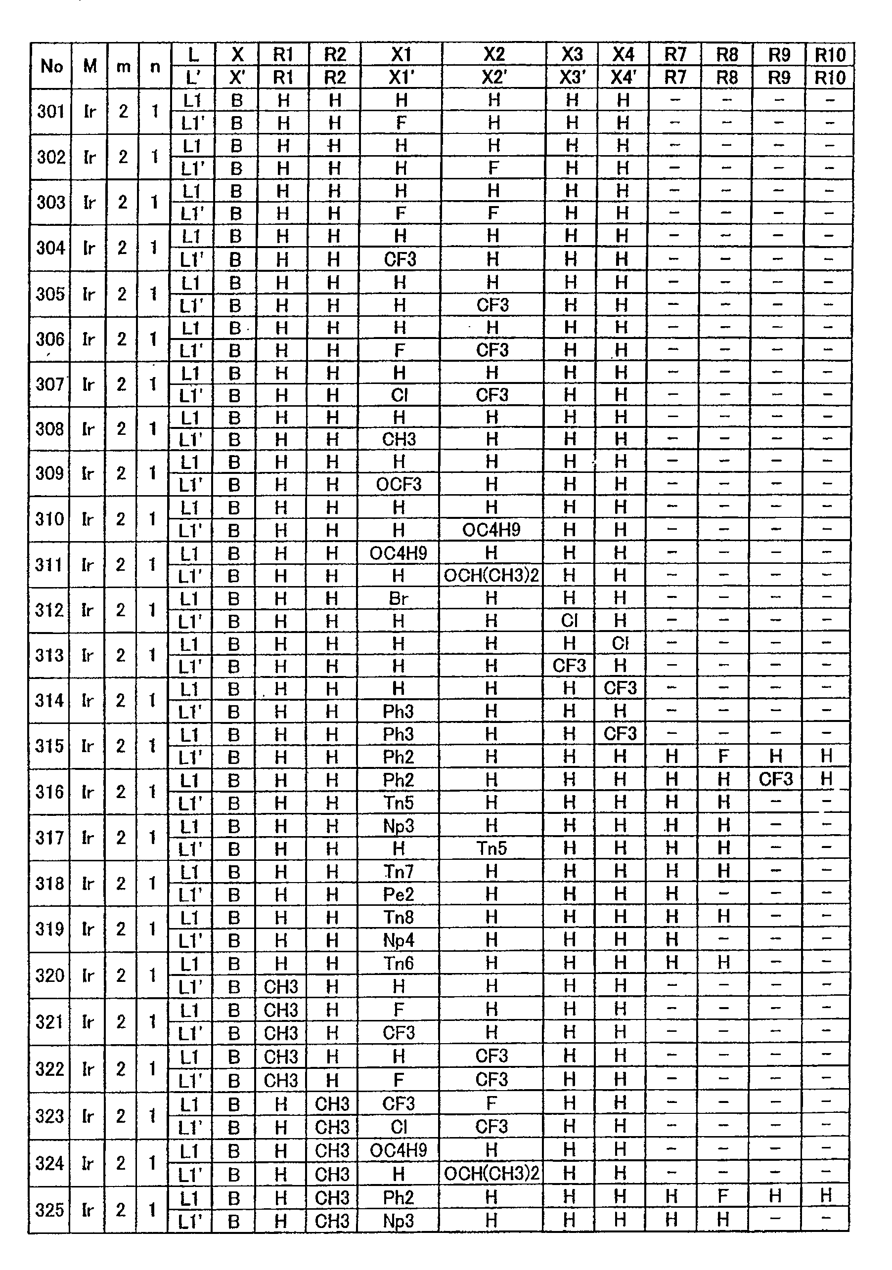
表1-8Table 1-8
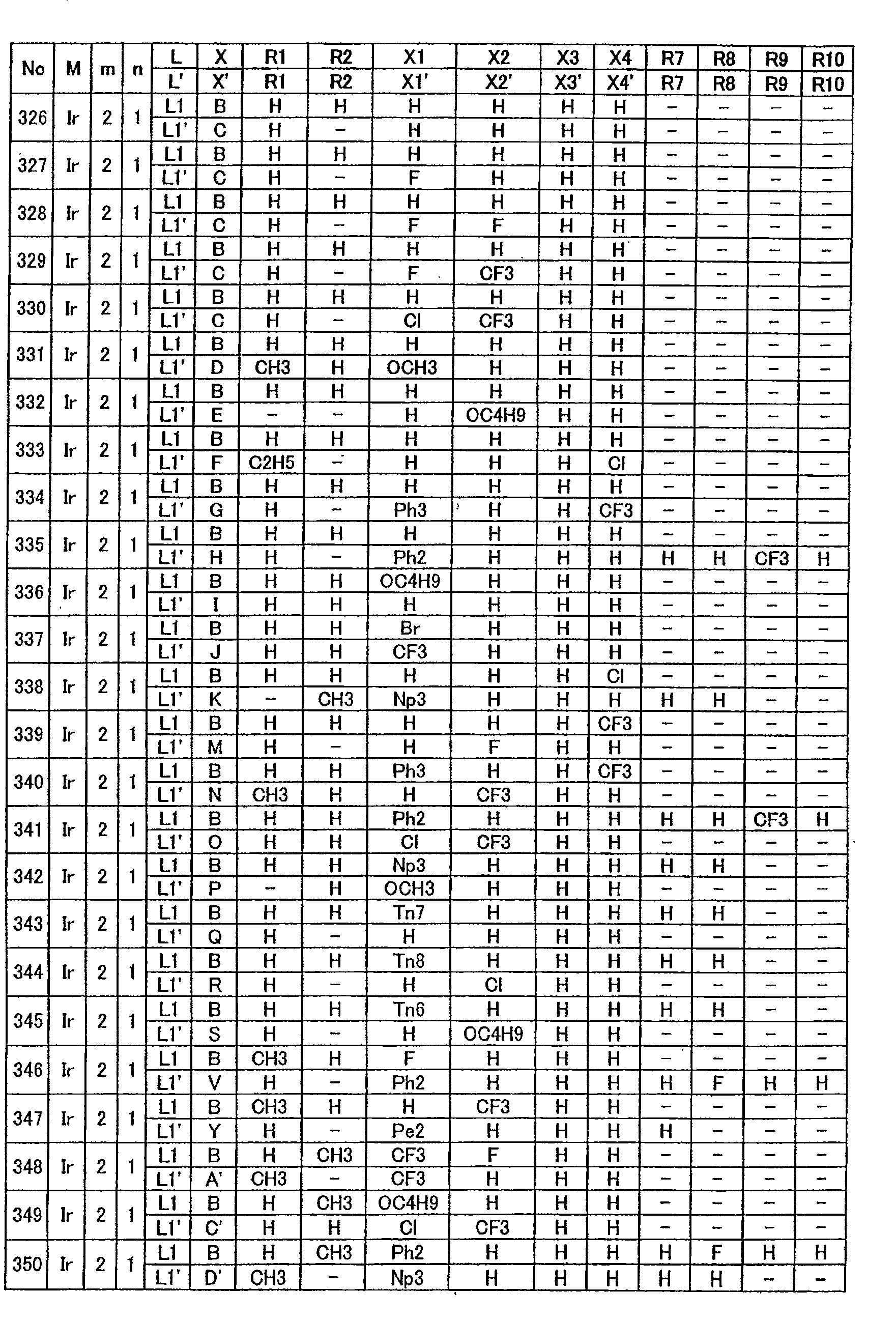
表1-9Table 1-9
表1-10Table 1-10
表1-11Table 1-11
表1-12Table 1-12

表1-13Table 1-13
表1-14Table 1-14
下面结合实施例解释本发明。The present invention is explained below in conjunction with embodiment.
<实施例1>(实例化合物No.1的合成)<Example 1> (Synthesis of Example Compound No.1)

在2升三颈烧瓶中放入69.0g(472mM)α-四氢萘酮(α-tetralon)、50.0g(720mM)盐酸羟胺、500ml乙醇和360ml 2N-氢氧化钠水溶液,在室温下搅拌1小时。在减压下除去溶剂得到残余物(干固体)。向该残余物中加入500ml水,然后用乙酸乙酯萃取三遍,每次使用150ml乙酸乙酯。用无水硫酸镁使有机层干燥,然后在减压下除去溶剂,得到74g α-四氢萘酮=肟的浅黄色晶体(收率:97.2%)。Put 69.0g (472mM) α-tetralone (α-tetralon), 50.0g (720mM) hydroxylamine hydrochloride, 500ml ethanol and 360ml 2N-sodium hydroxide aqueous solution in 2 liters of three-necked flasks, stir at room temperature for 1 Hour. The solvent was removed under reduced pressure to give a residue (dry solid). To the residue was added 500 ml of water, followed by extraction three times with 150 ml of ethyl acetate each time. The organic layer was dried with anhydrous magnesium sulfate, and then the solvent was removed under reduced pressure to obtain 74 g of pale yellow crystals of α-tetralone=oxime (yield: 97.2%).

在1升三巯烧瓶中放入80ml四氢呋喃和23.8g(595mM)60%-含油的氢化钠,在室温下搅拌5分钟,然后在15分钟内滴加至74g(459mM)α-四氢萘酮=肟在500ml无水DMF(二甲基甲酰胺)溶液中。然后将所述混合物在室温下搅拌1小时,向其中加入113.5g(939mM)烯丙基溴,然后在室温下搅拌12小时。反应后,使反应产物减压干燥得到残余物。向该残余物中加入500ml水,然后用乙酸乙酯萃取三遍,每次使用200ml乙酸乙酯。用无水硫酸镁使有机层干燥,然后在减压下除去溶剂,得到棕色液体。使该液体减压蒸馏得到79.5g(收率:86.0%)α-四氢萘酮=肟=O-烯丙基=醚(沸点=75-80℃(6.7Pa))。Put 80ml tetrahydrofuran and 23.8g (595mM) 60%-oily sodium hydride in a 1-liter ammercapto flask, stir at room temperature for 5 minutes, then add dropwise to 74g (459mM) α-tetralone in 15 minutes = Oxime in 500 ml dry DMF (dimethylformamide) solution. The mixture was then stirred at room temperature for 1 hour, and 113.5 g (939 mM) of allyl bromide was added thereto, followed by stirring at room temperature for 12 hours. After the reaction, the reaction product was dried under reduced pressure to obtain a residue. To the residue was added 500 ml of water, followed by extraction three times with 200 ml of ethyl acetate each time. The organic layer was dried over anhydrous magnesium sulfate, and then the solvent was removed under reduced pressure to obtain a brown liquid. The liquid was distilled under reduced pressure to obtain 79.5 g (yield: 86.0%) of α-tetralone=oxime=O-allyl=ether (boiling point=75-80° C. (6.7 Pa)).

在1升高压釜中放入58.0g(288mM)α-四氢萘酮=肟=O-烯丙基=醚,充以氧气后,气密地密封,然后在190℃下剧烈搅拌5天。使该液体冷却至室温得到高粘性棕色液体,使之溶于氯仿,用5%盐酸萃取三遍(每次300ml)。用48%氢氧化钠使含水层碱化,用氯仿萃取三遍(每次350ml)。用无水硫酸镁使有机层干燥,然后在减压下蒸发。残余物通过硅胶柱色谱法(洗脱剂:氯仿)提纯,通过硅胶柱色谱法(洗脱剂:己烷/乙酸乙酯=5/1)进一步提纯,得到7.7g浅棕色液体。所述液体通过Kugelroh蒸馏器提纯得到6.6g无色的苯并-[h]-5,6-二氢喹啉(收率:12.6%)。Put 58.0g (288mM) α-tetralone=oxime=O-allyl=ether in a 1-liter autoclave, fill it with oxygen, seal it airtightly, and stir vigorously at 190°C for 5 days. The liquid was cooled to room temperature to obtain a highly viscous brown liquid, which was dissolved in chloroform and extracted three times with 5% hydrochloric acid (300 ml each time). The aqueous layer was basified with 48% sodium hydroxide and extracted three times with chloroform (350 mL each). The organic layer was dried over anhydrous magnesium sulfate, and then evaporated under reduced pressure. The residue was purified by silica gel column chromatography (eluent: chloroform), and further purified by silica gel column chromatography (eluent: hexane/ethyl acetate=5/1) to obtain 7.7 g of light brown liquid. The liquid was purified by a Kugelroh distiller to obtain 6.6 g of colorless benzo-[h]-5,6-dihydroquinoline (yield: 12.6%).

在100ml四巯烧瓶中放入50ml甘油,在搅拌并用氮气鼓泡下于130-140℃加热2小时。通过静置使所述甘油冷却至100℃,向其中加入0.91g(5.02mM)苯并-[h]-5,6-二氢喹啉和0.50g(1.02mM)乙酰丙酮合铱(III),然后在氮气流中于190-215℃加热搅拌5小时。使反应产物冷却至室温,倒入300ml 1N盐酸中。过滤回收沉淀物,水洗,溶于丙酮以通过过滤除去不溶物。在减压下除去丙酮得到残余物,通过硅胶柱色谱法(洗脱剂:氯仿)提纯,得到0.11g三{苯并-[h]-5,6-二氢喹啉}合铱(III)的黄色粉末(收率:14.7%)。Put 50ml of glycerin in a 100ml four-mercapto flask, and heat at 130-140°C for 2 hours while stirring and bubbling with nitrogen. The glycerol was cooled to 100° C. by standing, and 0.91 g (5.02 mM) of benzo-[h]-5,6-dihydroquinoline and 0.50 g (1.02 mM) of iridium(III) acetylacetonate were added thereto , and then heated and stirred at 190-215° C. for 5 hours in a nitrogen stream. The reaction product was cooled to room temperature and poured into 300 ml of 1N hydrochloric acid. The precipitate was recovered by filtration, washed with water, and dissolved in acetone to remove insoluble matter by filtration. Acetone was removed under reduced pressure to obtain a residue, which was purified by silica gel column chromatography (eluent: chloroform) to obtain 0.11 g of tri{benzo-[h]-5,6-dihydroquinoline}iridium(III) of yellow powder (yield: 14.7%).
该化合物的溶液显示出*max(最大或峰发射波长)为511nm而量子产量为0.51的PL(光致发光)光谱。作为对照,测量与所述金属配位化合物不同的未用亚甲基交联的上述传统发光材料Ir(ppy)3的溶液的PL光谱时,该材料显示*max(最大发射波长)为510nm而量子产量为0.40。此外,通过施加电场,后面所述实施例3中得到的有机EL装置产生高发光度的激发光。而且其EL光谱*max(最大发射波长)为510nm。A solution of this compound exhibits a PL (photoluminescence) spectrum with a *max (maximum or peak emission wavelength) of 511 nm and a quantum yield of 0.51. As a control, when measuring the PL spectrum of a solution of the above-mentioned conventional luminescent material Ir(ppy) that is not crosslinked with methylene, which is different from the metal coordination compound, the material shows that *max (maximum emission wavelength) is 510 nm and The quantum yield is 0.40. In addition, the organic EL device obtained in Example 3 described later generates excitation light with high luminosity by applying an electric field. And its EL spectrum *max (maximum emission wavelength) is 510nm.
<实施例2>(实例化合物No.53的合成)<Example 2> (Synthesis of Example Compound No.53)

在3升三巯烧瓶中放入166.0g(1036mM)1-苯并环庚酮、125.0g(1141mM)盐酸O-烯丙基羟胺、93.5g(1140mM)乙酸钠、158.0g(1143mM)碳酸钾和1500ml乙醇,于80℃加热搅拌1.5小时。使反应产物冷却至室温,在减压下除去溶剂得到残余物。向该残余物中加1500ml水,然后用乙酸乙酯萃取三遍(每次500ml)。用无水硫酸镁使有机层干燥,然后在减压下除去溶剂得到浅棕色液体。使该液体在减压下蒸馏得到221.8g(收率:99.0%)1-苯并环庚酮=肟=O-烯丙基=醚(沸点=75-83℃(4.0Pa))。Put 166.0g (1036mM) 1-benzocycloheptanone, 125.0g (1141mM) O-allyl hydroxylamine hydrochloride, 93.5g (1140mM) sodium acetate, 158.0g (1143mM) potassium carbonate in a 3-liter ammercapto flask and 1500ml of ethanol, heated and stirred at 80°C for 1.5 hours. The reaction product was cooled to room temperature, and the solvent was removed under reduced pressure to obtain a residue. To the residue was added 1500 ml of water, followed by extraction three times with ethyl acetate (500 ml each). The organic layer was dried over anhydrous magnesium sulfate, and then the solvent was removed under reduced pressure to obtain a light brown liquid. The liquid was distilled under reduced pressure to obtain 221.8 g (yield: 99.0%) of 1-benzocycloheptanone=oxime=O-allyl=ether (boiling point=75-83° C. (4.0 Pa)).

在5升高压釜中放入220.0g(1022mM)1-苯并环庚酮=肟=O-烯丙基=醚,充以氧气后,气密地密封,然后在190℃下剧烈搅拌3天。使该液体冷却至室温得到高粘性棕色液体,使之溶于2升氯仿,用5%盐酸萃取三遍(每次500ml)。用48%氢氧化钠使含水层碱化,用氯仿萃取三遍(每次500ml)。用无水硫酸镁使有机层干燥,然后通过硅胶柱色谱法(洗脱剂:己烷/乙酸乙酯=5/1)提纯,得到19g浅棕色液体。所述液体通过Kugelroh蒸馏器提纯得到13.5g 3,2’-亚丙基-2-苯基吡啶的浅绿色液体(收率:13.5%)。Put 220.0g (1022mM) 1-benzocycloheptanone=oxime=O-allyl=ether in a 5-liter autoclave, fill it with oxygen, seal it airtightly, and stir vigorously at 190°C for 3 days . The liquid was cooled to room temperature to obtain a highly viscous brown liquid, which was dissolved in 2 liters of chloroform and extracted three times with 5% hydrochloric acid (500 ml each time). The aqueous layer was basified with 48% sodium hydroxide and extracted three times with chloroform (500 ml each). The organic layer was dried over anhydrous magnesium sulfate, and then purified by silica gel column chromatography (eluent: hexane/ethyl acetate=5/1) to obtain 19 g of a light brown liquid. The liquid was purified by a Kugelroh distiller to obtain 13.5 g of 3,2'-propylene-2-phenylpyridine as a pale green liquid (yield: 13.5%).

在100ml四巯烧瓶中放入50ml甘油,在搅拌并用氮气鼓泡下于130-140℃加热2小时。通过静置使所述甘油冷却至100℃,向其中加入0.98g(5.02mM)3,2’-亚丙基-2-苯基吡啶和0.50g(1.02mM)乙酰丙酮合铱(III),然后在氮气流中于190-215℃加热搅拌8小时。使反应产物冷却至室温,倒入300ml 1N盐酸中。过滤回收沉淀物,水洗,溶于丙酮以通过过滤除去不溶物。在减压下除去丙酮得到残余物,通过硅胶柱色谱法(洗脱剂:氯仿)提纯,得到0.18g三{3,2’-亚丙基-2-苯基吡啶}合铱(III)的黄色粉末(收率:22.7%)。Put 50ml of glycerin in a 100ml four-mercapto flask, and heat at 130-140°C for 2 hours while stirring and bubbling with nitrogen. The glycerin was cooled to 100° C. by standing, 0.98 g (5.02 mM) of 3,2′-propylene-2-phenylpyridine and 0.50 g (1.02 mM) of iridium(III) acetylacetonate were added thereto, Then heated and stirred at 190-215° C. for 8 hours in a nitrogen flow. The reaction product was cooled to room temperature and poured into 300 ml of 1N hydrochloric acid. The precipitate was recovered by filtration, washed with water, and dissolved in acetone to remove insoluble matter by filtration. Acetone was removed under reduced pressure to obtain a residue, which was purified by silica gel column chromatography (eluent: chloroform) to obtain 0.18 g of tri{3,2'-propylene-2-phenylpyridine}iridium(III) Yellow powder (yield: 22.7%).
通过施加电场,后面所述实施例6中得到的有机EL装置产生蓝绿色的激发光。The organic EL device obtained in Example 6 described later generates blue-green excitation light by applying an electric field.
<实施例3-11和对比例1><Examples 3-11 and Comparative Example 1>
用有图1(b)所示三层结构有机层的装置作为装置结构。在玻璃基板(透明基板15)上形成100nm厚的ITO(氧化锡铟)薄膜(透明电极14),然后制作布线图。在真空室(10-4Pa)内用电阻加热通过真空(气相)沉积相继在所述形成ITO的基板上形成如下所示有机层和金属电极层。A device having a three-layer structure organic layer as shown in Fig. 1(b) was used as the device structure. A 100 nm-thick ITO (indium tin oxide) film (transparent electrode 14) was formed on a glass substrate (transparent substrate 15), and then a wiring pattern was produced. An organic layer and a metal electrode layer as shown below were sequentially formed on the ITO-formed substrate by vacuum (vapor phase) deposition in a vacuum chamber (10 -4 Pa) with resistance heating.
有机层1(空穴迁移层13)(40nm):α-NPDOrganic layer 1 (hole transport layer 13) (40nm): α-NPD
有机层2(发光层12)(20nm):CBP:发光材料(95:5)的混合物Organic layer 2 (luminescent layer 12) (20nm): CBP: mixture of luminescent material (95:5)
该层通过作为主体材料的CBP与重量比为5wt%的作为发光材料的下表2中所示金属配位化合物共沉积形成。This layer was formed by co-deposition of CBP as a host material and metal complexes shown in Table 2 below as a light-emitting material in a weight ratio of 5 wt%.
有机层3(电子迁移层16)(30nm):Alq3Organic layer 3 (electron transport layer 16) (30nm): Alq3
金属电极层1(金属电极11)(15nm):Al-Li合金(Li=1.8wt%)Metal electrode layer 1 (metal electrode 11) (15nm): Al-Li alloy (Li=1.8wt%)
金属电极层2(金属电极11)(100nm):AlMetal electrode layer 2 (metal electrode 11) (100nm): Al
形成电极材料层之后,进行布线以提供3mm2的电极面积。After forming the electrode material layer, wiring was performed to provide an electrode area of 3 mm 2 .
向有ITO电极(作为阳极)和Al电极(作为阴极)的各发光装置施加电场(电压)以给每个装置提供相同的电流值,测量发光度(亮度)随时间的变化。电流量设定为70mA/cm2,初期各装置显示出在80-250cd/m2范围内的发光度。这些发光度值降至其1/2需要一段时间。An electric field (voltage) was applied to each light-emitting device having an ITO electrode (as an anode) and an Al electrode (as a cathode) to supply each device with the same current value, and changes in luminosity (brightness) over time were measured. The amount of current was set at 70 mA/cm 2 , and initially each device showed a luminosity in the range of 80-250 cd/m 2 . It takes a while for these luminosity values to drop to 1/2 of their value.
为测量,将各发光装置从真空室中取出,在干燥氮气流气氛中进行测量以消除装置衰退因素如氧气和湿气(水分)。For the measurement, each light-emitting device was taken out from the vacuum chamber, and the measurement was performed in a dry nitrogen flow atmosphere to eliminate device degradation factors such as oxygen and humidity (moisture).
对比例1中,使用上述论文2中所述Ir(ppy)3作为传统发光材料。In Comparative Example 1, the Ir(ppy) 3 described in the above paper 2 was used as the traditional luminescent material.
使用各化合物的连续供能试验装置的结果示于表2中。与使用传统发光材料的装置相比,使用本发明金属配位化合物的发光装置提供较长的发光度半衰期,从而导致基于本发明材料的良好稳定性的具有高耐久性的装置。Table 2 shows the results of the continuous energy supply test apparatus using each compound. Compared to devices using conventional luminescent materials, light emitting devices using the metal complexes of the invention provide longer luminosity half-lives, resulting in devices with high durability based on the good stability of the materials of the invention.
表2Table 2
<实施例12><Example 12>
结合图2,描述本发明电致发光装置用于采用图3所示TFT电路的活性基体型彩色有机EL显示器的实施方案。Referring to FIG. 2, the embodiment of the electroluminescence device of the present invention applied to the active matrix type color organic EL display using the TFT circuit shown in FIG. 3 will be described.
图2示意地说明装配有机EL装置和驱动装置的面板结构的例子。该实施方案中,像素数量为128×128像素。顺便提及,一个像素由绿色像素、蓝色像素和红色像素组成的三色像素构成。FIG. 2 schematically illustrates an example of a panel structure equipped with an organic EL device and a driving device. In this embodiment, the number of pixels is 128*128 pixels. Incidentally, one pixel is composed of three-color pixels consisting of green pixels, blue pixels, and red pixels.
在玻璃基板上,按已知方式用多晶硅形成薄膜晶体管电路(称为“TFT电路”)。On a glass substrate, a thin film transistor circuit (referred to as "TFT circuit") is formed using polysilicon in a known manner.
在与所述每一彩色像素对应的区域,用硬掩模通过真空沉积形成以下所示厚度的有机层和金属电极层,然后制作布线图。以下示出与各像素对应的有机层的结构。In the region corresponding to each color pixel, an organic layer and a metal electrode layer with the thickness shown below are formed by vacuum deposition using a hard mask, and then a wiring pattern is made. The structure of the organic layer corresponding to each pixel is shown below.
绿色像素:α-NPD(40nm)/CBP:磷光材料(=93:7重量比)(30nm)/BCP(20nm)/Alq(40nm)Green pixel: α-NPD(40nm)/CBP:phosphorescent material (=93:7 weight ratio)(30nm)/BCP(20nm)/Alq(40nm)
蓝色像素:α-NPD(50nm)/BCP(20nm)/Alq(50nm)Blue pixel: α-NPD(50nm)/BCP(20nm)/Alq(50nm)
红色像素:α-NPD(40nm)/CBP:PtOEP(=93:7重量比)(30nm)/BCP(20nm)/Alq(40nm)Red pixel: α-NPD(40nm)/CBP:PtOEP(=93:7 weight ratio)(30nm)/BCP(20nm)/Alq(40nm)
所述绿色像素的发光层是通过作为主体材料的CBP与重量比为7%的磷光材料(实例化合物No.1)共沉积形成的。The light-emitting layer of the green pixel was formed by co-deposition of CBP as a host material and a phosphorescent material (Example Compound No. 1) at a weight ratio of 7%.
图2所示面板中,配置扫描信号驱动器、数据信号驱动器和电流供应源,分别与门选择线(gate selection lines)、数据信号线和供电线相连。在门选择线和数据信号线的交叉点,设置图3中所示像素电路(等效电路)。扫描信号驱动器顺序选择门扫描线G1、G2、G3、…、Gn,与之同步地由数据信号驱动器提供图像信号。In the panel shown in Figure 2, a scan signal driver, a data signal driver, and a current supply source are configured, and are respectively connected to gate selection lines, data signal lines, and power supply lines. At the intersection of the gate selection line and the data signal line, a pixel circuit (equivalent circuit) shown in FIG. 3 is provided. The scanning signal driver sequentially selects the gate scanning lines G1, G2, G3, .
下面结合图3中所示等效电路描述像素电路操作。当给门选择线施加选择信号时,打开TFT1使得由数据信号线向电容器Cadd供应显示信号,从而测定TFT2的门电位。根据TFT2的门电位通过供电线向在各像素配置的有机发光装置部分(缩写为EL)供应电流。在一个帧周期内使TFT2的门电位保持在Cadd,以致该周期内所述电流连续地从供电线流入EL装置部分。从而,在一个帧周期内保持发光。The pixel circuit operation is described below with reference to the equivalent circuit shown in FIG. 3 . When a selection signal is applied to the gate selection line, TFT1 is turned on so that a display signal is supplied from the data signal line to capacitor Cadd, thereby measuring the gate potential of TFT2. The organic light emitting device portion (abbreviated as EL) arranged in each pixel is supplied with current through the power supply line according to the gate potential of the TFT2. The gate potential of the TFT 2 is kept at Cadd for one frame period, so that the current continuously flows from the power supply line into the EL device portion during this period. Thus, light emission is maintained for one frame period.
结果证明可显示所要图像信息,而且发现稳定地显示良好的图像。As a result, it was confirmed that desired image information could be displayed, and it was found that a good image was stably displayed.
该实施方案中,尽管将采用TFT电路的活性基体型驱动方案用于所述显示器,但本发明所用开关装置不必特殊限制,甚至单晶硅基板、MIM(金属-绝缘体-金属)装置、a-Si(无定形硅)TFT电路等也可很容易地用于所述显示器。In this embodiment, although an active matrix type driving scheme using a TFT circuit is used for the display, the switching device used in the present invention does not have to be particularly limited, even a single crystal silicon substrate, a MIM (metal-insulator-metal) device, a- Si (amorphous silicon) TFT circuits and the like can also be easily used for the display.
工业实用性Industrial Applicability
如上所述,用本发明上述式(1)所示金属配位化合物作发光材料的发光装置可提供高发光效率并长时间保持高亮度的发光。此外,所述材料是能调节发射波长特别是提供较短波长的优异材料。本发明发光装置作为显示设备也极好。As mentioned above, the light-emitting device using the metal complex compound represented by the above formula (1) of the present invention as a light-emitting material can provide high light-emitting efficiency and maintain high-brightness light for a long time. Furthermore, the material is an excellent material for tuning the emission wavelength, especially to provide shorter wavelengths. The light-emitting device of the present invention is also excellent as a display device.
本发明所示高效发光装置适用于要求节能和高亮度的产品。作为应用实例,可列举用于显示设备、照明设备、印刷机的光源和液晶显示设备的背光。作为显示设备,可提供能节能、分辨率高或重量减轻的平面显示器。此外,作为印刷机的光源,可用本发明发光装置代替目前广泛使用的激光束印刷机的激光源部分。通过以矩阵形式独立地排列可寻址装置和相对于感光鼓进行所要求的曝光形成图像。用本发明装置可显著地减小设备体积(尺寸)。The high-efficiency light-emitting device shown in the present invention is suitable for products requiring energy saving and high brightness. As application examples, light sources for display devices, lighting devices, printing machines, and backlights for liquid crystal display devices can be cited. As a display device, a flat display capable of energy saving, high resolution, or weight reduction can be provided. In addition, as a light source of a printing machine, the light-emitting device of the present invention can be used instead of the laser light source portion of a laser beam printing machine widely used at present. An image is formed by individually arranging addressable devices in a matrix and performing the required exposure with respect to a photosensitive drum. The equipment volume (dimensions) can be significantly reduced by using the device of the present invention.
Claims (2)

Applications Claiming Priority (2)
| Application Number | Priority Date | Filing Date | Title |
|---|---|---|---|
| JP190662/2001 | 2001-06-25 | ||
| JP2001190662A JP2003007469A (en) | 2001-06-25 | 2001-06-25 | Light emitting element and display device |
Publications (2)
| Publication Number | Publication Date |
|---|---|
| CN1503785A CN1503785A (en) | 2004-06-09 |
| CN100500656C true CN100500656C (en) | 2009-06-17 |
Family
ID=19029400
Family Applications (1)
| Application Number | Title | Priority Date | Filing Date |
|---|---|---|---|
| CNB028087011A Expired - Fee Related CN100500656C (en) | 2001-06-25 | 2002-06-17 | Metal coordination compound and electroluminescence device |
Country Status (8)
| Country | Link |
|---|---|
| US (2) | US6824894B2 (en) |
| EP (1) | EP1400514B1 (en) |
| JP (1) | JP2003007469A (en) |
| KR (1) | KR100747060B1 (en) |
| CN (1) | CN100500656C (en) |
| AT (1) | ATE422493T1 (en) |
| DE (1) | DE60231117D1 (en) |
| WO (1) | WO2003000661A1 (en) |
Cited By (2)
| Publication number | Priority date | Publication date | Assignee | Title |
|---|---|---|---|---|
| CN107849077A (en) * | 2015-07-30 | 2018-03-27 | 默克专利有限公司 | Bridged electroluminescent metal complexes for use in electronic devices |
| CN109232309A (en) * | 2018-10-15 | 2019-01-18 | 安徽绩溪县徽煌化工有限公司 | A kind of processing method improving 1-tetralone oxime output capacity and purifying |
Families Citing this family (84)
| Publication number | Priority date | Publication date | Assignee | Title |
|---|---|---|---|---|
| JP4438042B2 (en) * | 2001-03-08 | 2010-03-24 | キヤノン株式会社 | Metal coordination compound, electroluminescent element and display device |
| JP2003007469A (en) * | 2001-06-25 | 2003-01-10 | Canon Inc | Light emitting element and display device |
| US7238435B2 (en) * | 2001-09-04 | 2007-07-03 | Canon Kabushiki Kaisha | Polymeric compound and organic luminescence device |
| JP3890242B2 (en) * | 2002-03-26 | 2007-03-07 | キヤノン株式会社 | Polymer compound and electroluminescent device |
| JP2003332074A (en) * | 2002-05-09 | 2003-11-21 | Canon Inc | Light emitting device using metal coordination compound |
| EP1549112A4 (en) * | 2002-09-20 | 2009-01-07 | Idemitsu Kosan Co | ORGANIC ELECTROLUMINESCENT ELEMENT |
| EP2248870B1 (en) | 2002-11-26 | 2018-12-26 | Konica Minolta Holdings, Inc. | Organic electroluminscent element and display and illuminator |
| US7198730B2 (en) | 2003-08-28 | 2007-04-03 | E. I. Du Pont De Nemours And Company | Phosphorescent material |
| JP4455211B2 (en) * | 2003-08-29 | 2010-04-21 | キヤノン株式会社 | Light emitting element and display device |
| DE10345572A1 (en) * | 2003-09-29 | 2005-05-19 | Covion Organic Semiconductors Gmbh | metal complexes |
| US7279232B2 (en) * | 2004-01-26 | 2007-10-09 | Universal Display Corporation | Electroluminescent stability |
| JP4378186B2 (en) * | 2004-02-06 | 2009-12-02 | キヤノン株式会社 | Organic EL element array |
| US7709100B2 (en) * | 2004-07-07 | 2010-05-04 | Universal Display Corporation | Electroluminescent efficiency |
| TW200614865A (en) * | 2004-08-23 | 2006-05-01 | Nippon Steel Chemical Co | Organic electroluminescent element |
| JP4478555B2 (en) * | 2004-11-30 | 2010-06-09 | キヤノン株式会社 | Metal complex, light emitting element and image display device |
| TW200634020A (en) * | 2004-12-09 | 2006-10-01 | Merck Patent Gmbh | Metal complexes |
| EP1844060B1 (en) * | 2005-02-03 | 2010-11-17 | Merck Patent GmbH | Metal complexes |
| US7498437B2 (en) * | 2005-04-27 | 2009-03-03 | Au Optronics Corporation | Phosphorescent light-emitting device with doped iridium-complex |
| US7851072B2 (en) * | 2005-05-19 | 2010-12-14 | Universal Display Corporation | Stable and efficient electroluminescent materials |
| WO2007004380A1 (en) | 2005-07-01 | 2007-01-11 | Konica Minolta Holdings, Inc. | Organic electroluminescent element material, organic electroluminescent element, display device, and lighting equipment |
| DE102005032332A1 (en) * | 2005-07-08 | 2007-01-11 | Merck Patent Gmbh | metal complexes |
| US20100177264A1 (en) * | 2005-08-15 | 2010-07-15 | Sumitomo Checmical Company, Limited | Light-emitting material containing metal complex and photoelectric device using same |
| WO2007029466A1 (en) * | 2005-09-06 | 2007-03-15 | Konica Minolta Holdings, Inc. | Organic electroluminescent device, display and illuminating device |
| WO2007028417A1 (en) * | 2005-09-07 | 2007-03-15 | Technische Universität Braunschweig | Triplett emitter having condensed five-membered rings |
| CN100362006C (en) * | 2005-09-16 | 2008-01-16 | 中国科学院长春应用化学研究所 | Dendritic iridium complex and organic electroluminescent device using the compound |
| KR101359362B1 (en) * | 2005-12-02 | 2014-02-07 | 가부시키가이샤 한도오따이 에네루기 켄큐쇼 | Semiconductor device, display device, and electronic device |
| JP2007173584A (en) * | 2005-12-22 | 2007-07-05 | Canon Inc | Light emitting device |
| DE102006006412A1 (en) * | 2006-02-13 | 2007-08-16 | Merck Patent Gmbh | Electronic component, process for its production and its use |
| WO2007097149A1 (en) | 2006-02-20 | 2007-08-30 | Konica Minolta Holdings, Inc. | Organic electroluminescence element, white light emitting element, display device and illuminating device |
| US20090043064A1 (en) * | 2006-02-22 | 2009-02-12 | Sumitomo Chemical Company, Limited | Metal complex, polymer compound, and device containing it |
| US20090091253A1 (en) | 2006-03-17 | 2009-04-09 | Konica Minolta Holdings, Inc. | Organic electroluminescent element, display device and lighting device |
| EP2615153B1 (en) | 2006-03-23 | 2017-03-01 | Konica Minolta Holdings, Inc. | Organic electroluminescent device, display and illuminating device |
| JP2007269735A (en) * | 2006-03-31 | 2007-10-18 | Canon Inc | Metal complex, light emitting element and display device |
| US9118020B2 (en) | 2006-04-27 | 2015-08-25 | Global Oled Technology Llc | Electroluminescent devices including organic eil layer |
| JP2007302565A (en) * | 2006-05-08 | 2007-11-22 | Canon Inc | Metal complex, light emitting element and image display device |
| JP2008007500A (en) * | 2006-06-02 | 2008-01-17 | Canon Inc | Metal complex and organic light emitting device |
| JP2007335614A (en) | 2006-06-15 | 2007-12-27 | Canon Inc | Organic electroluminescent device and display device |
| JP4965914B2 (en) * | 2006-07-05 | 2012-07-04 | キヤノン株式会社 | Organic compound and light emitting device |
| US7736756B2 (en) * | 2006-07-18 | 2010-06-15 | Global Oled Technology Llc | Light emitting device containing phosphorescent complex |
| JP5127206B2 (en) * | 2006-11-28 | 2013-01-23 | キヤノン株式会社 | Metal complex compound, organic light emitting device and display device |
| JP2008141000A (en) * | 2006-12-01 | 2008-06-19 | Canon Inc | Organic light emitting device |
| US20130032785A1 (en) * | 2011-08-01 | 2013-02-07 | Universal Display Corporation | Materials for organic light emitting diode |
| JP2008288254A (en) * | 2007-05-15 | 2008-11-27 | Canon Inc | Organic EL device |
| JP5053713B2 (en) * | 2007-05-30 | 2012-10-17 | キヤノン株式会社 | Phosphorescent material, organic electroluminescent element and image display device using the same |
| US8034465B2 (en) * | 2007-06-20 | 2011-10-11 | Global Oled Technology Llc | Phosphorescent oled having double exciton-blocking layers |
| WO2009006550A1 (en) | 2007-07-05 | 2009-01-08 | Nitto Denko Corporation | Light emitting devices and compositions |
| JP5305637B2 (en) | 2007-11-08 | 2013-10-02 | キヤノン株式会社 | Organometallic complex, organic light emitting device using the same, and display device |
| US20090191427A1 (en) * | 2008-01-30 | 2009-07-30 | Liang-Sheng Liao | Phosphorescent oled having double hole-blocking layers |
| JP5472121B2 (en) | 2009-01-28 | 2014-04-16 | コニカミノルタ株式会社 | ORGANIC ELECTROLUMINESCENT ELEMENT, DISPLAY DEVICE AND LIGHTING DEVICE, AND METHOD FOR PRODUCING ORGANIC ELECTROLUMINESCENT ELEMENT |
| EP3046156A1 (en) | 2009-02-06 | 2016-07-20 | Konica Minolta Holdings, Inc. | Organic electroluminescent element, and illumination device and display device each comprising the element |
| EP2453496B1 (en) | 2009-07-07 | 2018-11-14 | Konica Minolta Holdings, Inc. | Organic electroluminescent element, novel compound, lighting device and display device |
| US20120211707A1 (en) | 2009-08-27 | 2012-08-23 | National Inst. Of Adv. Ind. Sci. And Tech. | Metal complex composition and complex polymer |
| EP2471800B1 (en) | 2009-08-27 | 2014-01-15 | National Institute of Advanced Industrial Science And Technology | Iridium complex and light emitting material formed from same |
| CN102812573B (en) | 2010-03-23 | 2015-09-30 | 默克专利有限公司 | For the material of organic electroluminescence device |
| WO2011134013A1 (en) * | 2010-04-28 | 2011-11-03 | Commonwealth Scientific And Industrial Research Organisation | Electroluminescent devices based on phosphorescent iridium and related group viii metal multicyclic compounds |
| TW201223956A (en) * | 2010-08-13 | 2012-06-16 | Solvay | Light emitting materials for electronics |
| US9923154B2 (en) | 2011-02-16 | 2018-03-20 | Konica Minolta, Inc. | Organic electroluminescent element, lighting device, and display device |
| GB201107917D0 (en) * | 2011-05-12 | 2011-06-22 | Cambridge Display Tech Ltd | Organic light emitting material and device |
| JP5742586B2 (en) | 2011-08-25 | 2015-07-01 | コニカミノルタ株式会社 | Organic electroluminescence element, lighting device and display device |
| JP6052182B2 (en) | 2011-11-14 | 2016-12-27 | コニカミノルタ株式会社 | Organic electroluminescence device and planar light emitter |
| JP5880274B2 (en) | 2012-05-21 | 2016-03-08 | コニカミノルタ株式会社 | Organic electroluminescence element, lighting device and display device |
| JP5849867B2 (en) | 2012-06-21 | 2016-02-03 | コニカミノルタ株式会社 | Organic electroluminescence element, display device and lighting device |
| JP6242905B2 (en) * | 2012-10-09 | 2017-12-06 | メルク パテント ゲーエムベーハー | Metal complex |
| KR101995191B1 (en) | 2012-12-10 | 2019-07-02 | 코니카 미놀타 가부시키가이샤 | Material for organic electroluminescent element, organic electroluminescent element, illumination device, and display device |
| WO2014092014A1 (en) | 2012-12-10 | 2014-06-19 | コニカミノルタ株式会社 | Organic electroluminescence element, illumination device and display device |
| JP5911418B2 (en) | 2012-12-27 | 2016-04-27 | キヤノン株式会社 | Organic light emitting device |
| JP5911419B2 (en) | 2012-12-27 | 2016-04-27 | キヤノン株式会社 | Organic light emitting device and display device |
| JP5818870B2 (en) | 2012-12-27 | 2015-11-18 | キヤノン株式会社 | Organic light emitting device and display device |
| JP6071569B2 (en) | 2013-01-17 | 2017-02-01 | キヤノン株式会社 | Organic light emitting device |
| JP6222931B2 (en) | 2013-01-21 | 2017-11-01 | キヤノン株式会社 | Organic light emitting device |
| JP5984689B2 (en) | 2013-01-21 | 2016-09-06 | キヤノン株式会社 | Organometallic complex and organic light emitting device using the same |
| JP6095390B2 (en) | 2013-02-06 | 2017-03-15 | キヤノン株式会社 | Organic light emitting device and display device |
| GB2515491B (en) * | 2013-06-24 | 2015-11-18 | Cambridge Display Tech Ltd | Phosphorescent light-emitting compounds and their use in light-emitting devices |
| JP6372084B2 (en) * | 2014-01-22 | 2018-08-15 | セイコーエプソン株式会社 | Light emitting device and electronic device |
| KR102418886B1 (en) * | 2014-12-29 | 2022-07-08 | 엘지디스플레이 주식회사 | Phosphorescent compound and Light emitting diode and Display device using the same |
| US11555048B2 (en) * | 2016-12-01 | 2023-01-17 | Universal Display Corporation | Organic electroluminescent materials and devices |
| CN109790193B (en) * | 2016-12-13 | 2022-03-22 | 广州华睿光电材料有限公司 | Transition metal complex, application thereof, mixture and organic electronic device |
| US10745431B2 (en) * | 2017-03-08 | 2020-08-18 | Universal Display Corporation | Organic electroluminescent materials and devices |
| GB2564490A (en) * | 2017-07-14 | 2019-01-16 | Sumitomo Chemical Co | Light-emitting compound |
| KR102568783B1 (en) * | 2018-03-22 | 2023-08-22 | 삼성디스플레이 주식회사 | Organometallic compound, organic light emitting device comprising the same and organic emitting apparatus comprising the organic light emitting device |
| KR102792008B1 (en) | 2018-08-16 | 2025-04-08 | 듀폰스페셜티머터리얼스코리아 유한회사 | Organic electroluminescent compound and organic electroluminescent device comprising the same |
| CN113544135B (en) * | 2019-03-11 | 2022-11-01 | 东丽株式会社 | Pyrromethene metal complex, light-emitting element material, light-emitting element, display device, and lighting device |
| US12240865B2 (en) | 2019-03-27 | 2025-03-04 | Universal Display Corporation | Organic electroluminescent materials and devices |
| US12122793B2 (en) | 2019-03-27 | 2024-10-22 | Universal Display Corporation | Organic electroluminescent materials and devices |
Family Cites Families (15)
| Publication number | Priority date | Publication date | Assignee | Title |
|---|---|---|---|---|
| JP2000005859A (en) * | 1998-06-19 | 2000-01-11 | Toshiba Corp | Electronic equipment, manufacturing method thereof, and mold apparatus |
| AU3908400A (en) | 1999-03-23 | 2000-10-09 | University Of Southern California | Cyclometallated metal complexes as phosphorescent dopants in organic leds |
| KR100946314B1 (en) * | 1999-12-01 | 2010-03-09 | 더 트러스티즈 오브 프린스턴 유니버시티 | Organic light emitting device comprising a phosphorescent organo metallic compound |
| JP2001181616A (en) * | 1999-12-27 | 2001-07-03 | Fuji Photo Film Co Ltd | Light emitting element material composed of orthometalated palladium complex and light emitting element |
| JP2001181617A (en) | 1999-12-27 | 2001-07-03 | Fuji Photo Film Co Ltd | Light emitting element material composed of orthometalated palladium complex and light emitting element |
| US6821645B2 (en) * | 1999-12-27 | 2004-11-23 | Fuji Photo Film Co., Ltd. | Light-emitting material comprising orthometalated iridium complex, light-emitting device, high efficiency red light-emitting device, and novel iridium complex |
| US20020121638A1 (en) * | 2000-06-30 | 2002-09-05 | Vladimir Grushin | Electroluminescent iridium compounds with fluorinated phenylpyridines, phenylpyrimidines, and phenylquinolines and devices made with such compounds |
| JP3345719B2 (en) * | 2000-07-04 | 2002-11-18 | コナミ株式会社 | Game control method, game device, and recording medium |
| CN101924190B (en) * | 2000-08-11 | 2012-07-04 | 普林斯顿大学理事会 | Organometallic compounds and emission-shifting organic electrophosphorescence |
| JP4154139B2 (en) * | 2000-09-26 | 2008-09-24 | キヤノン株式会社 | Light emitting element |
| JP4154140B2 (en) * | 2000-09-26 | 2008-09-24 | キヤノン株式会社 | Metal coordination compounds |
| JP4460743B2 (en) * | 2000-09-29 | 2010-05-12 | 富士フイルム株式会社 | Method for producing iridium complex or tautomer thereof |
| CN1285601C (en) * | 2000-11-30 | 2006-11-22 | 佳能株式会社 | Light emitting devices and displays |
| JP4154145B2 (en) | 2000-12-01 | 2008-09-24 | キヤノン株式会社 | Metal coordination compound, light emitting device and display device |
| JP2003007469A (en) * | 2001-06-25 | 2003-01-10 | Canon Inc | Light emitting element and display device |
-
2001
- 2001-06-25 JP JP2001190662A patent/JP2003007469A/en active Pending
-
2002
- 2002-06-17 AT AT02738730T patent/ATE422493T1/en not_active IP Right Cessation
- 2002-06-17 DE DE60231117T patent/DE60231117D1/en not_active Expired - Lifetime
- 2002-06-17 WO PCT/JP2002/006001 patent/WO2003000661A1/en not_active Ceased
- 2002-06-17 CN CNB028087011A patent/CN100500656C/en not_active Expired - Fee Related
- 2002-06-17 KR KR1020037016545A patent/KR100747060B1/en not_active Expired - Fee Related
- 2002-06-17 US US10/181,342 patent/US6824894B2/en not_active Expired - Lifetime
- 2002-06-17 EP EP02738730A patent/EP1400514B1/en not_active Expired - Lifetime
-
2004
- 2004-09-17 US US10/942,861 patent/US7078115B2/en not_active Expired - Fee Related
Cited By (3)
| Publication number | Priority date | Publication date | Assignee | Title |
|---|---|---|---|---|
| CN107849077A (en) * | 2015-07-30 | 2018-03-27 | 默克专利有限公司 | Bridged electroluminescent metal complexes for use in electronic devices |
| CN107849077B (en) * | 2015-07-30 | 2021-02-26 | 默克专利有限公司 | Electroluminescent metal complexes for bridging in electronic devices |
| CN109232309A (en) * | 2018-10-15 | 2019-01-18 | 安徽绩溪县徽煌化工有限公司 | A kind of processing method improving 1-tetralone oxime output capacity and purifying |
Also Published As
| Publication number | Publication date |
|---|---|
| JP2003007469A (en) | 2003-01-10 |
| WO2003000661A1 (en) | 2003-01-03 |
| KR100747060B1 (en) | 2007-08-07 |
| US6824894B2 (en) | 2004-11-30 |
| US20030235712A1 (en) | 2003-12-25 |
| CN1503785A (en) | 2004-06-09 |
| US7078115B2 (en) | 2006-07-18 |
| ATE422493T1 (en) | 2009-02-15 |
| KR20040010735A (en) | 2004-01-31 |
| US20050085654A1 (en) | 2005-04-21 |
| DE60231117D1 (en) | 2009-03-26 |
| EP1400514A1 (en) | 2004-03-24 |
| EP1400514A4 (en) | 2005-04-13 |
| EP1400514B1 (en) | 2009-02-11 |
Similar Documents
| Publication | Publication Date | Title |
|---|---|---|
| CN100500656C (en) | Metal coordination compound and electroluminescence device | |
| JP4307001B2 (en) | Metal coordination compound, electroluminescent element and display device | |
| JP4438042B2 (en) | Metal coordination compound, electroluminescent element and display device | |
| JP4154145B2 (en) | Metal coordination compound, light emitting device and display device | |
| JP4154140B2 (en) | Metal coordination compounds | |
| JP4307000B2 (en) | Metal coordination compound, electroluminescent element and display device | |
| JP4006335B2 (en) | Light emitting element and display device | |
| JP4478555B2 (en) | Metal complex, light emitting element and image display device | |
| EP1191613B1 (en) | Luminescence device, display apparatus and metal coordination compound | |
| JP5403105B2 (en) | Organic electroluminescence element material and organic electroluminescence element | |
| JP5127206B2 (en) | Metal complex compound, organic light emitting device and display device | |
| US20020094453A1 (en) | Metal coordination compound, luminescence device and display apparatus | |
| JP2003342284A (en) | Metal coordination compound, light emitting element and display device | |
| JP2002234894A (en) | Metal coordination compound, light emitting element and display device | |
| JP2007302565A (en) | Metal complex, light emitting element and image display device | |
| JP4935001B2 (en) | Organic electroluminescence element material | |
| JP2005170851A (en) | Metal coordination compound, organic light emitting device, and image display device | |
| JPWO2005097941A1 (en) | ORGANIC ELECTROLUMINESCENT ELEMENT MATERIAL, ORGANIC ELECTROLUMINESCENT ELEMENT, DISPLAY DEVICE AND LIGHTING DEVICE |
Legal Events
| Date | Code | Title | Description |
|---|---|---|---|
| C06 | Publication | ||
| PB01 | Publication | ||
| C10 | Entry into substantive examination | ||
| SE01 | Entry into force of request for substantive examination | ||
| C14 | Grant of patent or utility model | ||
| GR01 | Patent grant | ||
| CF01 | Termination of patent right due to non-payment of annual fee | ||
| CF01 | Termination of patent right due to non-payment of annual fee |
Granted publication date: 20090617 Termination date: 20190617 |