CN100487878C - Method of fabricating semiconductor device and semiconductor fabricated by the same method - Google Patents
Method of fabricating semiconductor device and semiconductor fabricated by the same method Download PDFInfo
- Publication number
- CN100487878C CN100487878C CNB2005100640649A CN200510064064A CN100487878C CN 100487878 C CN100487878 C CN 100487878C CN B2005100640649 A CNB2005100640649 A CN B2005100640649A CN 200510064064 A CN200510064064 A CN 200510064064A CN 100487878 C CN100487878 C CN 100487878C
- Authority
- CN
- China
- Prior art keywords
- temperature
- layer
- silicon layer
- under
- pressure
- Prior art date
- Legal status (The legal status is an assumption and is not a legal conclusion. Google has not performed a legal analysis and makes no representation as to the accuracy of the status listed.)
- Expired - Lifetime
Links
Images


Classifications
-
- H—ELECTRICITY
- H10—SEMICONDUCTOR DEVICES; ELECTRIC SOLID-STATE DEVICES NOT OTHERWISE PROVIDED FOR
- H10D—INORGANIC ELECTRIC SEMICONDUCTOR DEVICES
- H10D30/00—Field-effect transistors [FET]
- H10D30/01—Manufacture or treatment
- H10D30/021—Manufacture or treatment of FETs having insulated gates [IGFET]
- H10D30/031—Manufacture or treatment of FETs having insulated gates [IGFET] of thin-film transistors [TFT]
- H10D30/0312—Manufacture or treatment of FETs having insulated gates [IGFET] of thin-film transistors [TFT] characterised by the gate electrodes
- H10D30/0314—Manufacture or treatment of FETs having insulated gates [IGFET] of thin-film transistors [TFT] characterised by the gate electrodes of lateral top-gate TFTs comprising only a single gate
-
- H—ELECTRICITY
- H10—SEMICONDUCTOR DEVICES; ELECTRIC SOLID-STATE DEVICES NOT OTHERWISE PROVIDED FOR
- H10D—INORGANIC ELECTRIC SEMICONDUCTOR DEVICES
- H10D30/00—Field-effect transistors [FET]
- H10D30/01—Manufacture or treatment
- H10D30/021—Manufacture or treatment of FETs having insulated gates [IGFET]
- H10D30/031—Manufacture or treatment of FETs having insulated gates [IGFET] of thin-film transistors [TFT]
- H10D30/0312—Manufacture or treatment of FETs having insulated gates [IGFET] of thin-film transistors [TFT] characterised by the gate electrodes
- H10D30/0316—Manufacture or treatment of FETs having insulated gates [IGFET] of thin-film transistors [TFT] characterised by the gate electrodes of lateral bottom-gate TFTs comprising only a single gate
-
- H—ELECTRICITY
- H10—SEMICONDUCTOR DEVICES; ELECTRIC SOLID-STATE DEVICES NOT OTHERWISE PROVIDED FOR
- H10D—INORGANIC ELECTRIC SEMICONDUCTOR DEVICES
- H10D30/00—Field-effect transistors [FET]
- H10D30/01—Manufacture or treatment
- H10D30/021—Manufacture or treatment of FETs having insulated gates [IGFET]
- H10D30/031—Manufacture or treatment of FETs having insulated gates [IGFET] of thin-film transistors [TFT]
- H10D30/0321—Manufacture or treatment of FETs having insulated gates [IGFET] of thin-film transistors [TFT] comprising silicon, e.g. amorphous silicon or polysilicon
-
- H10P14/24—
-
- H10P14/3411—
-
- H10P14/3808—
Landscapes
- Recrystallisation Techniques (AREA)
- Thin Film Transistor (AREA)
Abstract
公开了一种半导体器件的制造方法以及通过该方法制造的半导体器件。所述方法包括:使用等离子体增强化学气相沉积(PECVD)法和低压化学气相沉积(LPCVD)法中的任何一种方法在衬底上沉积包含非晶硅的硅层;在预定温度下、H2O气氛中退火所述硅层,以形成多晶硅层;在所述多晶硅层上形成栅极绝缘层;在所述多晶硅层中形成杂质区以界定所述源极区和漏极区;以及激活所述杂质区。因此,可以提供一种半导体器件,其中防止了衬底弯曲并且构成半导体层的多晶硅极佳。
Disclosed are a method of manufacturing a semiconductor device and a semiconductor device manufactured by the method. The method includes: depositing a silicon layer comprising amorphous silicon on a substrate using any one of a plasma-enhanced chemical vapor deposition (PECVD) method and a low-pressure chemical vapor deposition (LPCVD) method; at a predetermined temperature, H annealing the silicon layer in a 2 O atmosphere to form a polysilicon layer; forming a gate insulating layer on the polysilicon layer; forming an impurity region in the polysilicon layer to define the source region and the drain region; and activating the impurity region. Therefore, it is possible to provide a semiconductor device in which the substrate is prevented from warping and polysilicon constituting the semiconductor layer is excellent.
Description
技术领域 technical field
本发明涉及一种半导体器件的制造方法,更具体而言,涉及一种通过其可防止衬底弯曲的半导体器件的制造方法以及通过该方法所制造的半导体器件。The present invention relates to a method of manufacturing a semiconductor device, and more particularly, to a method of manufacturing a semiconductor device by which warpage of a substrate can be prevented and a semiconductor device manufactured by the method.
背景技术 Background technique
多晶硅用于有机发光显示装置的有源器件,通常为薄膜晶体管(TFT),所述薄膜晶体管用于向像素区域和外围驱动区域提供电流。Polysilicon is used in active devices of organic light-emitting display devices, usually thin film transistors (TFTs), which are used to supply current to pixel regions and peripheral driving regions.
通常,通过非晶硅的结晶来形成多晶硅。Generally, polysilicon is formed by crystallization of amorphous silicon.
通常,依据结晶温度,例如参照约500℃,用于结晶的方法可大体分为低温结晶法和高温结晶法。Generally, methods for crystallization can be roughly classified into low-temperature crystallization methods and high-temperature crystallization methods depending on the crystallization temperature, for example, referring to about 500°C.
使用准分子激光器的准分子激光退火(ELA)法主要用作低温结晶法。准分子激光退火法可使用玻璃衬底,因为其在约450℃的结晶温度下进行。然而,制造成本高并且衬底在最佳尺寸方面受到限制,由此增加了制造显示装置的总成本。An excimer laser annealing (ELA) method using an excimer laser is mainly used as a low-temperature crystallization method. The excimer laser annealing method can use a glass substrate because it is performed at a crystallization temperature of about 450°C. However, the manufacturing cost is high and the substrate is limited in optimum size, thereby increasing the overall cost of manufacturing the display device.
高温结晶法包括固相结晶法、快速热退火法等。低成本的退火法被广泛用作高温结晶法。High-temperature crystallization methods include solid-phase crystallization, rapid thermal annealing, and the like. Low-cost annealing methods are widely used as high-temperature crystallization methods.
然而,由于固相结晶法需要在高于600℃的温度下加热20或更长时间以用于结晶,在结晶的多晶硅中包含许多晶体缺陷。因此,不能获得足够的电场迁移率,衬底易于在退火工艺、即热处理工艺期间变形,并且降低的结晶温度降低了生产率。因为固相结晶法也在高结晶温度下执行,所以不能使用玻璃衬底。However, since the solid phase crystallization method requires heating at a temperature higher than 600° C. for 20 or more time for crystallization, many crystal defects are contained in crystallized polysilicon. Therefore, sufficient electric field mobility cannot be obtained, the substrate is easily deformed during the annealing process, that is, the heat treatment process, and the lowered crystallization temperature lowers productivity. Since the solid phase crystallization method is also performed at a high crystallization temperature, a glass substrate cannot be used.
同时,尽管快速热退火(RTA)法可以以相对短的时间完成,但衬底易于由于严重的热冲击而变形,并且结晶的多晶硅具有较差的电特性。Meanwhile, although the rapid thermal annealing (RTA) method can be completed in a relatively short time, the substrate is easily deformed due to severe thermal shock, and crystallized polysilicon has poor electrical characteristics.
因此,在结晶时需要使用低成本的高温退火法,以降低制造有源器件的成本。而且,需要使用廉价玻璃衬底的高温退火法,通过该方法玻璃衬底不弯曲并且结晶度极佳。Therefore, a low-cost high-temperature annealing method needs to be used during crystallization to reduce the cost of manufacturing active devices. Also, a high-temperature annealing method using an inexpensive glass substrate by which the glass substrate does not bend and is excellent in crystallinity is required.
发明内容 Contents of the invention
因此,通过提供一种半导体器件的制造方法以及通过该方法制造的半导体器件,本发明解决了与传统器件相关的上述问题,所述方法能够使多晶硅以极佳的结晶度结晶并防止衬底在结晶时由于高的结晶温度而弯曲。Accordingly, the present invention solves the above-mentioned problems associated with conventional devices by providing a method of manufacturing a semiconductor device capable of crystallizing polysilicon with excellent crystallinity and preventing the substrate from being It bends during crystallization due to the high crystallization temperature.
在本发明的一个示例性实施例中,半导体器件的制造方法包括:使用等离子体增强化学气相沉积(PECVD)法或低压化学气相沉积(LPCVD)法在衬底上沉积包含非晶硅的硅层;在预定温度下、H2O气氛中退火所述硅层,以形成多晶硅层;在所述多晶硅层上形成栅极绝缘层;在所述多晶硅层中形成杂质区;以及激活所述杂质区。In an exemplary embodiment of the present invention, a method for manufacturing a semiconductor device includes: depositing a silicon layer comprising amorphous silicon on a substrate using a plasma-enhanced chemical vapor deposition (PECVD) method or a low-pressure chemical vapor deposition (LPCVD) method ; annealing the silicon layer at a predetermined temperature in an H 2 O atmosphere to form a polysilicon layer; forming a gate insulating layer on the polysilicon layer; forming an impurity region in the polysilicon layer; and activating the impurity region .
在本发明的另一示例性实施例中,半导体器件的制造方法包括:使用等离子体增强化学气相沉积(PECVD)法或低压化学气相沉积(LPCVD)法在衬底上沉积包含非晶硅的硅层;用杂质离子掺杂所述硅层以界定源极区和漏极区;构图所述非晶硅以形成半导体层;在所述衬底上方、所述半导体层上形成栅极绝缘层;在所述栅极绝缘层上形成栅电极,所述栅电极对应于所述半导体层的沟道区;以及在预定温度下、H2O气氛中退火所述非晶硅层,从而使所述非晶硅结晶并激活所述杂质离子。In another exemplary embodiment of the present invention, a method for manufacturing a semiconductor device includes: depositing silicon containing amorphous silicon on a substrate using a plasma-enhanced chemical vapor deposition (PECVD) method or a low-pressure chemical vapor deposition (LPCVD) method. layer; doping the silicon layer with impurity ions to define a source region and a drain region; patterning the amorphous silicon to form a semiconductor layer; forming a gate insulating layer on the semiconductor layer above the substrate; forming a gate electrode on the gate insulating layer, the gate electrode corresponding to the channel region of the semiconductor layer; and annealing the amorphous silicon layer at a predetermined temperature in an H 2 O atmosphere, thereby making the Amorphous silicon crystallizes and activates the impurity ions.
在本发明的又一示例性实施例中,半导体器件的制造方法包括:在衬底上形成栅电极;在所述衬底上方、所述栅电极上形成栅极绝缘层;使用等离子体增强化学气相沉积(PECVD)法或低压化学气相沉积(LPCVD)法在所述栅极绝缘层上沉积包含非晶硅的硅层;将杂质离子掺杂到所述硅层中使用光致抗蚀剂以界定源极区和漏极区;以及去除所述光致抗蚀剂,然后在确定的温度下、H2O气氛中退火所述非晶硅,从而使所述非晶硅结晶并激活所述杂质离子。In yet another exemplary embodiment of the present invention, a method for manufacturing a semiconductor device includes: forming a gate electrode on a substrate; forming a gate insulating layer over the substrate and on the gate electrode; using plasma-enhanced chemical Depositing a silicon layer containing amorphous silicon on the gate insulating layer by vapor phase deposition (PECVD) or low pressure chemical vapor deposition (LPCVD); doping impurity ions into the silicon layer using a photoresist to defining a source region and a drain region; and removing the photoresist, and then annealing the amorphous silicon at a certain temperature in an H 2 O atmosphere, thereby crystallizing the amorphous silicon and activating the Impurity ions.
在本发明的又一示例性实施例中,通过所述方法制造半导体器件,其中所述半导体器件是薄膜晶体管。In yet another exemplary embodiment of the present invention, a semiconductor device is manufactured by the method, wherein the semiconductor device is a thin film transistor.
附图说明 Description of drawings
现将参照附图并参考其某些示例性实施例描述本发明的上述和其他特征,附图中:The above and other features of the invention will now be described with reference to the accompanying drawings, and with reference to certain exemplary embodiments thereof, in which:
图1A至1E顺序说明了根据本发明第一实施例的半导体器件的制造方法;1A to 1E sequentially illustrate a method of manufacturing a semiconductor device according to a first embodiment of the present invention;
图2A至2E顺序说明了根据本发明第二实施例的半导体器件的制造方法;2A to 2E sequentially illustrate a method of manufacturing a semiconductor device according to a second embodiment of the present invention;
图3A至3D顺序说明了根据本发明第三实施例的半导体器件的制造方法;3A to 3D sequentially illustrate a method of manufacturing a semiconductor device according to a third embodiment of the present invention;
图4说明了通过本发明的实施例制造的多晶硅薄膜的FWHM。Figure 4 illustrates the FWHM of a polysilicon thin film fabricated by an embodiment of the present invention.
具体实施方式 Detailed ways
以下将参照附图更充分地描述本发明,附图中表示了本发明的实施例。在附图中,为了清楚起见,夸大了层和区域的厚度。The present invention will be described more fully hereinafter with reference to the accompanying drawings, in which embodiments of the invention are shown. In the drawings, the thicknesses of layers and regions are exaggerated for clarity.
图1A至1E顺序说明了根据本发明第一实施例的半导体器件的制造方法。1A to 1E sequentially illustrate a method of manufacturing a semiconductor device according to a first embodiment of the present invention.
参照图1A,在衬底10上沉积非晶硅层或包含大量非晶硅的硅层12。此时,通常所使用的绝缘和透明玻璃衬底用作衬底10。Referring to FIG. 1A , an amorphous silicon layer or a
使用通常的沉积方法、如等离子体增强化学气相沉积(PECVD)法或低压化学气相沉积(LPCVD)法来沉积硅层12。使用SiH4+Ar和/或H2,在1至1.5Torr的压力下和约330至约430℃的温度下执行PECVD法。此外,使用Si2H6+Ar,在0.2至0.4Torr的压力下和约400至约500℃的温度下执行LPCVD法。The
另外,为了防止在衬底中产生的污染物或类似物扩散到硅层中,或者为了增强硅层和衬底之间的界面特性,在沉积非晶硅层之前,可在衬底上进一步形成缓冲层,如氮化硅(SiNx)层或氧化硅(SiO2)层。In addition, in order to prevent contamination or the like generated in the substrate from diffusing into the silicon layer, or to enhance the interface characteristics between the silicon layer and the substrate, before depositing the amorphous silicon layer, further forming A buffer layer, such as a silicon nitride (SiNx) layer or a silicon oxide (SiO 2 ) layer.
然后退火非晶硅层或包含大量非晶硅的硅层12,如图1B所示。此时,当加热硅层时,非晶硅熔化。同时,非晶硅冷却并结晶为多晶硅。然后构图多晶硅以形成半导体层12a。The amorphous silicon layer or
在本发明中,快速热退火(RTA)工艺或在炉中的通常的高温退火工艺用作退火工艺。传统的退火在惰性N2或O2气氛中进行,而本发明中的退火在H2O气氛中进行。In the present invention, a rapid thermal annealing (RTA) process or a general high temperature annealing process in a furnace is used as the annealing process. Traditional annealing is performed in an inert N 2 or O 2 atmosphere, while the annealing in the present invention is performed in an H 2 O atmosphere.
与N2或O2气氛中的退火相比,H2O气氛中的退火在相同温度的条件下缩短了退火时间,在相同时间的条件下降低了退火温度。Compared with the annealing in N 2 or O 2 atmosphere, the annealing in H 2 O atmosphere shortens the annealing time under the same temperature condition, and reduces the annealing temperature under the same time condition.
更具体而言,作为透明绝缘衬底的传统玻璃衬底由于高温而弯曲,而本发明的衬底不会弯曲,因为退火温度可被降低。More specifically, a conventional glass substrate as a transparent insulating substrate is warped due to high temperature, but the substrate of the present invention does not warp because the annealing temperature can be lowered.
在本发明中,退火温度优选在550至750℃的范围内,更优选地,退火温度在600至710℃的范围内,因为可以以适当的退火时间获得极佳的多晶硅。当退火温度低于550℃时,可能不能实现结晶,当退火温度高于750℃时,衬底会弯曲。In the present invention, the annealing temperature is preferably in the range of 550 to 750°C, and more preferably, the annealing temperature is in the range of 600 to 710°C because excellent polysilicon can be obtained with an appropriate annealing time. When the annealing temperature is lower than 550°C, crystallization may not be achieved, and when the annealing temperature is higher than 750°C, the substrate may warp.
此外,优选H2O的压力在10000Pa至2MPa的范围内。结晶速率与压力成比例,因此,当压力过低时,结晶速率变低并且退火时间变长,影响衬底。另一方面,过高的压力会导致爆炸。出于这些原因,对于退火,10000Pa至2MPa的压力是适合的。In addition, it is preferable that the pressure of H 2 O is in the range of 10000 Pa to 2 MPa. The crystallization rate is proportional to the pressure, therefore, when the pressure is too low, the crystallization rate becomes lower and the annealing time becomes longer, affecting the substrate. On the other hand, too high a pressure can cause an explosion. For these reasons, for annealing, a pressure of 10000 Pa to 2 MPa is suitable.
同时,优选将硅层沉积到小于2000埃的厚度。小的厚度有助于结晶。然而,当多晶硅用于形成薄膜晶体管时,过小的厚度会影响器件特性。因此,优选将硅层沉积到300至1000埃的厚度。At the same time, the silicon layer is preferably deposited to a thickness of less than 2000 Angstroms. A small thickness facilitates crystallization. However, when polysilicon is used to form a thin film transistor, an excessively small thickness may affect device characteristics. Therefore, the silicon layer is preferably deposited to a thickness of 300 to 1000 Angstroms.
如图1C所示,在半导体层12a上形成SiO2或SiNx的栅极绝缘层14。形成栅电极16,以对应于半导体层12a的有源沟道区100c,如图1D所示。As shown in FIG. 1C, a
使用栅电极16作为掩模,离子被掺杂到半导体层12a中,以形成源极区和漏极区100a和100b。通过准分子激光退火(ELA)工艺、RTA工艺或炉中的退火工艺,优选RTA或炉中的退火工艺,来激活掺杂由离子的半导体层12a,如图1E所示。Using the
接下来,在衬底的整个表面上方、栅电极16上形成层间绝缘层,如SiO2或SiNx。然后构图层间绝缘层以暴露源极区和漏极区100a和100b,并且形成源电极和漏电极,由此完成半导体器件。Next, an interlayer insulating layer such as SiO 2 or SiNx is formed over the entire surface of the substrate, on the
图2A至2E顺序说明了根据本发明第二实施例的半导体器件的制造方法。现将参照图2A至2E描述本发明的第二实施例。2A to 2E sequentially illustrate a method of manufacturing a semiconductor device according to a second embodiment of the present invention. A second embodiment of the present invention will now be described with reference to FIGS. 2A to 2E.
参照图2A,在衬底20上沉积非晶硅层或包含大量非晶硅的硅层22。此时,通常所使用的绝缘和透明玻璃衬底用作衬底20。Referring to FIG. 2A , an amorphous silicon layer or a
使用通常的沉积方法、如等离子体增强化学气相沉积(PECVD)法或低压化学气相沉积(LPCVD)法来沉积硅层。使用SiH4+Ar和/或H2,在1至1.5Torr的压力下和约330至约430℃的温度下执行PECVD法。此外,使用Si2H6+Ar,在0.2至0.4Torr的压力下和约400至约500℃的温度下执行LPCVD法。The silicon layer is deposited using conventional deposition methods such as plasma enhanced chemical vapor deposition (PECVD) or low pressure chemical vapor deposition (LPCVD). The PECVD method is performed at a pressure of 1 to 1.5 Torr and a temperature of about 330 to about 430° C. using SiH 4 +Ar and/or H 2 . In addition, the LPCVD method is performed at a pressure of 0.2 to 0.4 Torr and a temperature of about 400 to about 500° C. using Si 2 H 6 +Ar.
另外,为了防止在衬底中产生的污染物或类似物扩散到硅层中,或者为了增强硅层和衬底之间的界面特性,在沉积非晶硅层之前,可在衬底上进一步形成缓冲层,如SiNx或SiO2。In addition, in order to prevent contamination or the like generated in the substrate from diffusing into the silicon layer, or to enhance the interface characteristics between the silicon layer and the substrate, before depositing the amorphous silicon layer, further forming A buffer layer such as SiNx or SiO 2 .
然后在硅层22中的沟道区200c上、而不是之后将对应于源极区和漏极区200a和200b的区域上,涂敷光致抗蚀剂,并且将杂质离子注入到硅层22中。Then, on the
通过例如光刻和蚀刻工艺去除光致抗蚀剂,然后构图掺杂有杂质的硅层22,如图2B所示。The photoresist is removed by, for example, photolithography and etching processes, and then the impurity-doped
然后在图案化的硅层22上形成如SiO2或SiNx的无机绝缘层的栅极绝缘层24,如图2C所示。A
接下来,如图2D所示,在对应于沟道区200c的区域中形成栅极26,并进行退火。Next, as shown in FIG. 2D, the
在退火工艺期间,掺杂到源极区和漏极区200a和200b中的杂质离子被激活同时包含非晶硅的硅层22结晶为多晶硅层22a。During the annealing process, impurity ions doped into the source and
在本发明中,如快速热退火(RTA)工艺的通常高温退火工艺用作退火工艺。传统的退火在惰性N2或O2气氛中进行,而本发明中的退火在H2O气氛中进行。In the present invention, a general high temperature annealing process such as a rapid thermal annealing (RTA) process is used as the annealing process. Traditional annealing is performed in an inert N 2 or O 2 atmosphere, while the annealing in the present invention is performed in an H 2 O atmosphere.
与N2或O2气氛中的退火相比,H2O气氛中的退火在相同温度的条件下缩短了退火时间,在相同时间的条件下降低了退火温度。Compared with the annealing in N 2 or O 2 atmosphere, the annealing in H 2 O atmosphere shortens the annealing time under the same temperature condition, and reduces the annealing temperature under the same time condition.
更具体而言,作为透明绝缘衬底的传统玻璃衬底由于高温而弯曲,而本发明的衬底不会弯曲,因为退火温度可被降低。More specifically, a conventional glass substrate as a transparent insulating substrate is warped due to high temperature, but the substrate of the present invention does not warp because the annealing temperature can be lowered.
在本发明中,退火温度优选在550至750℃的范围内,更优选地,退火温度在600至710℃的范围内,因为可以以适当的退火时间获得极佳的多晶硅。当退火温度低于550℃时,可能不能实现结晶,当退火温度高于750℃时,衬底会弯曲。In the present invention, the annealing temperature is preferably in the range of 550 to 750°C, and more preferably, the annealing temperature is in the range of 600 to 710°C because excellent polysilicon can be obtained with an appropriate annealing time. When the annealing temperature is lower than 550°C, crystallization may not be achieved, and when the annealing temperature is higher than 750°C, the substrate may warp.
此外,优选H2O的压力在10000Pa至2MPa的范围内。结晶速率与压力成比例,因此,当压力过低时,结晶速率变低并且退火时间变长,影响衬底。另一方面,过高的压力会导致爆炸。出于这些原因,对于退火,10000Pa至2MPa的压力是适合的。In addition, it is preferable that the pressure of H 2 O is in the range of 10000 Pa to 2 MPa. The crystallization rate is proportional to the pressure, therefore, when the pressure is too low, the crystallization rate becomes lower and the annealing time becomes longer, affecting the substrate. On the other hand, too high a pressure can cause an explosion. For these reasons, for annealing, a pressure of 10000 Pa to 2 MPa is suitable.
同时,优选将硅层22沉积到小于2000埃的厚度。小的厚度有助于结晶。然而,当多晶硅用于形成薄膜晶体管时,过小的厚度会影响器件特性。因此,优选将硅层沉积到300至1000埃的厚度。At the same time,
尽管上述工艺足够获得多晶硅,但本发明可进一步包括一退火工艺以降低形成的多晶硅中的缺陷。Although the above process is sufficient to obtain polysilicon, the present invention may further include an annealing process to reduce defects in the formed polysilicon.
可通过准分子激光退火工艺或炉中的加热来执行所述进一步的退火工艺。The further annealing process may be performed by an excimer laser annealing process or heating in a furnace.
接下来,如图2E所示,在衬底的整个表面上方、栅电极26上形成层间绝缘层28,并且蚀刻层间绝缘层28以及栅极绝缘层24两者以形成接触孔,从而使源极区和漏极区200a和200b敞开。将金属填充到接触孔中以形成源电极和漏电极29a和29b,由此完成薄膜晶体管。Next, as shown in FIG. 2E, an
图3A至3D顺序说明了根据本发明第三实施例的半导体器件的制造方法。现将参照图3A至3D描述根据本发明第三实施例的半导体器件的制造方法。3A to 3D sequentially illustrate a method of manufacturing a semiconductor device according to a third embodiment of the present invention. A method of manufacturing a semiconductor device according to a third embodiment of the present invention will now be described with reference to FIGS. 3A to 3D .
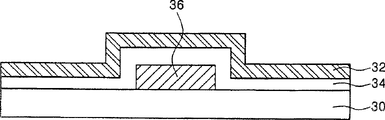
参照图3A,进行构图以在衬底30上形成栅电极36。此时,通常所使用的绝缘和透明玻璃衬底用作衬底30。Referring to FIG. 3A , patterning is performed to form a
另外,为了防止在衬底中产生的污染物或类似物扩散到电极中,或者为了增强衬底和电极之间的界面特性,可在衬底30上形成缓冲层,如SiNx或SiO2。In addition, a buffer layer such as SiNx or SiO2 may be formed on the
然后在衬底30的整个表面上方、栅电极36上形成如SiO2或SiNx的无机绝缘层的栅极绝缘层34。A
接下来,在栅极绝缘层34上沉积非晶硅层或包含大量非晶硅的硅层32,如图3B所示。Next, an amorphous silicon layer or a
使用通常的沉积方法、如等离子体增强化学气相沉积(PECVD)法或低压化学气相沉积(LPCVD)法来沉积硅层32。使用SiH4+Ar和/或H2,在1至1.5Torr的压力下和约330至约430℃的温度下执行PECVD法。此外,使用Si2H6+Ar,在0.2至0.4Torr的压力下和约400至约500℃的温度下执行LPCVD法。
然后在硅层32中的沟道区300c上、而不是之后将对应于源极区和漏极区300a和300b的区域上,涂敷光致抗蚀剂,并且将杂质离子注入到硅层32中,如图3C所示。A photoresist is then applied on the channel region 300c in the
接下来,进行退火。在退火工艺期间,掺杂到源极区和漏极区300a和300b中的杂质离子被激活同时包含非晶硅的硅层32结晶为多晶硅层32a。Next, annealing is performed. During the annealing process, impurity ions doped into the source and
在本发明中,如快速热退火(RTA)工艺的通常高温退火工艺用作退火工艺。传统的退火在惰性N2或O2气氛中进行,而本发明中的退火在H2O气氛中进行。In the present invention, a general high temperature annealing process such as a rapid thermal annealing (RTA) process is used as the annealing process. Traditional annealing is performed in an inert N 2 or O 2 atmosphere, while the annealing in the present invention is performed in an H 2 O atmosphere.
与N2或O2气氛中的退火相比,H2O气氛中的退火在相同温度的条件下缩短了退火时间,在相同时间的条件下降低了退火温度。Compared with the annealing in N 2 or O 2 atmosphere, the annealing in H 2 O atmosphere shortens the annealing time under the same temperature condition, and reduces the annealing temperature under the same time condition.
更具体而言,作为透明绝缘衬底的传统玻璃衬底由于高温而弯曲,而根据本发明的衬底不会弯曲,因为退火温度可被降低。More specifically, a conventional glass substrate as a transparent insulating substrate is warped due to high temperature, but the substrate according to the present invention does not warp because the annealing temperature can be lowered.
在本发明中,退火温度优选在550至750℃的范围内,更优选地,退火温度在600至710℃的范围内,因为可以以适当的退火时间获得极佳的多晶硅。当退火温度低于550℃时,可能不能实现结晶,当退火温度高于750℃时,衬底会弯曲。In the present invention, the annealing temperature is preferably in the range of 550 to 750°C, and more preferably, the annealing temperature is in the range of 600 to 710°C because excellent polysilicon can be obtained with an appropriate annealing time. When the annealing temperature is lower than 550°C, crystallization may not be achieved, and when the annealing temperature is higher than 750°C, the substrate may warp.
此外,优选H2O的压力在10000Pa至2MPa的范围内。结晶速率与压力成比例,因此,当压力过低时,结晶速率变低并且退火时间变长,影响衬底。另一方面,过高的压力会导致爆炸。出于这些原因,对于退火,10000Pa至2MPa的压力是适合的。In addition, it is preferable that the pressure of H 2 O is in the range of 10000 Pa to 2 MPa. The crystallization rate is proportional to the pressure, therefore, when the pressure is too low, the crystallization rate becomes lower and the annealing time becomes longer, affecting the substrate. On the other hand, too high a pressure can cause an explosion. For these reasons, for annealing, a pressure of 10000 Pa to 2 MPa is suitable.
同时,优选将硅层32沉积到小于2000埃的厚度。小的厚度有助于结晶。然而,当多晶硅用于形成薄膜晶体管时,过小的厚度会影响器件特性。因此,优选将硅层沉积到300至1000埃的厚度。At the same time,
尽管上述工艺足够获得多晶硅,但本发明可进一步包括一退火工艺以降低所形成的多晶硅中的缺陷。Although the above process is sufficient to obtain polysilicon, the present invention may further include an annealing process to reduce defects in the formed polysilicon.
可通过准分子激光退火工艺或炉中的加热来执行所述进一步的退火工艺。The further annealing process may be performed by an excimer laser annealing process or heating in a furnace.
在本发明中,所预期的是,所述半导体器件为薄膜晶体管。该薄膜晶体管可以是其中栅电极36形成在多晶硅层32a上方的顶部栅极薄膜晶体管,也可以是其中栅电极36形成在多晶硅层32a下方的底部栅极薄膜晶体管。In the present invention, it is contemplated that the semiconductor device is a thin film transistor. The TFT may be a top gate TFT in which the
下文中,提出了本发明的示例性实施例。然而,以下所述的实例仅仅意于辅助理解本发明,而并非限制本发明。Hereinafter, exemplary embodiments of the present invention are presented. However, the examples described below are only intended to assist understanding of the present invention, not to limit the present invention.
实例1至3Examples 1 to 3
在衬底上沉积厚度500埃的非晶硅层。作为沉积方法,在实例1中使用低压化学气相沉积(LPCVD)法,在实例2中使用包含2%或更少氢的等离子体增强化学气相沉积(PECVD)法,在实例3中使用包含10%或更多氢的等离子体增强化学气相沉积(PECVD)法。使用在710℃下小于10分钟的快速热退火(RTA)工艺退火非晶硅层并使其结晶。在H2O气氛中,使用O2或N2载气执行退火。所形成的多晶硅的拉曼谱如图4所示。A layer of amorphous silicon with a thickness of 500 Angstroms was deposited on the substrate. As the deposition method, the low-pressure chemical vapor deposition (LPCVD) method was used in Example 1, the plasma-enhanced chemical vapor deposition (PECVD) method containing 2% or less hydrogen was used in Example 2, and the plasma-enhanced chemical vapor deposition (PECVD) method containing 10% hydrogen was used in Example 3. or more hydrogen plasma enhanced chemical vapor deposition (PECVD) method. The amorphous silicon layer was annealed and crystallized using a rapid thermal annealing (RTA) process at 710° C. for less than 10 minutes. In an H2O atmosphere, perform annealing using O2 or N2 carrier gas. The Raman spectrum of the formed polysilicon is shown in FIG. 4 .
参照图4,可以看出,通过根据本发明的实例1至3退火非晶硅所得到的多晶硅具有极佳的结晶度,因为拉曼峰值的半高宽(FWHM)在4.5至7.5cm-1的范围内。考虑到通过通常方法制造的多晶硅具有大于8.0cm-1的拉曼峰值,可以看出,通过使用低压化学气相沉积(LPCVD)法或等离子体增强化学气相沉积(PECVD)法来沉积非晶硅,然后在H2O气氛中通过RTA工艺使所沉积的非晶硅结晶,本发明中的结晶度变得极佳。Referring to FIG. 4, it can be seen that the polysilicon obtained by annealing amorphous silicon according to Examples 1 to 3 of the present invention has excellent crystallinity because the full width at half maximum (FWHM) of the Raman peak is between 4.5 and 7.5 cm −1 In the range. Considering that polysilicon produced by a common method has a Raman peak greater than 8.0 cm −1 , it can be seen that by using a low-pressure chemical vapor deposition (LPCVD) method or a plasma-enhanced chemical vapor deposition (PECVD) method to deposit amorphous silicon, The deposited amorphous silicon is then crystallized by the RTA process in an H 2 O atmosphere, and the crystallinity in the present invention becomes excellent.
所制造的多晶硅薄膜适用于薄膜晶体管,而薄膜晶体管可用于平板显示装置,如有机发光显示装置或液晶显示装置。The manufactured polysilicon film is suitable for thin film transistors, and the thin film transistors can be used for flat panel display devices, such as organic light emitting display devices or liquid crystal display devices.
如上所述,根据本发明,当使用LPCVD或PECVD沉积非晶硅并使用固相结晶法使其结晶时,可以通过使用H2O退火气氛来降低退火时间和退火温度,由此防止工艺缺陷、如弯曲的衬底,并改善多晶硅的结晶度。As described above, according to the present invention, when amorphous silicon is deposited using LPCVD or PECVD and crystallized using a solid phase crystallization method, the annealing time and annealing temperature can be reduced by using an H2O annealing atmosphere, thereby preventing process defects, Such as curved substrates, and improve the crystallinity of polysilicon.
尽管已参照其某些示例性实施例描述了本发明,但本领域技术人员应理解的是,在不偏离由所附权利要求及其等同物所限定的本发明的主旨和范围的前提下,可以对本发明进行各种修改和变化。While the invention has been described with reference to certain exemplary embodiments thereof, it should be understood by those skilled in the art that, without departing from the spirit and scope of the invention as defined by the appended claims and their equivalents, Various modifications and changes can be made to the present invention.
本申请要求于2004年6月30日提交的韩国专利申请No.2004-50863的优先权,其全部内容在此引入作为参考。This application claims priority from Korean Patent Application No. 2004-50863 filed on Jun. 30, 2004, the entire contents of which are hereby incorporated by reference.
Claims (19)
Applications Claiming Priority (2)
| Application Number | Priority Date | Filing Date | Title |
|---|---|---|---|
| KR1020040050863A KR100666552B1 (en) | 2004-06-30 | 2004-06-30 | Manufacturing method of semiconductor device and semiconductor device manufactured by this method |
| KR50863/04 | 2004-06-30 |
Publications (2)
| Publication Number | Publication Date |
|---|---|
| CN1716552A CN1716552A (en) | 2006-01-04 |
| CN100487878C true CN100487878C (en) | 2009-05-13 |
Family
ID=35514519
Family Applications (1)
| Application Number | Title | Priority Date | Filing Date |
|---|---|---|---|
| CNB2005100640649A Expired - Lifetime CN100487878C (en) | 2004-06-30 | 2005-04-06 | Method of fabricating semiconductor device and semiconductor fabricated by the same method |
Country Status (4)
| Country | Link |
|---|---|
| US (1) | US7696030B2 (en) |
| JP (1) | JP4188330B2 (en) |
| KR (1) | KR100666552B1 (en) |
| CN (1) | CN100487878C (en) |
Families Citing this family (11)
| Publication number | Priority date | Publication date | Assignee | Title |
|---|---|---|---|---|
| US20070042536A1 (en) * | 2005-08-17 | 2007-02-22 | Chi-Wen Chen | Thin film transistor and method for manufacturing the same |
| KR100810638B1 (en) * | 2006-12-06 | 2008-03-07 | 삼성에스디아이 주식회사 | Thin film transistor, manufacturing method thereof and organic light emitting display device having same |
| KR20080067158A (en) * | 2007-01-15 | 2008-07-18 | 삼성전자주식회사 | Display |
| KR101015847B1 (en) | 2008-01-18 | 2011-02-23 | 삼성모바일디스플레이주식회사 | Thin film transistor, manufacturing method thereof and organic light emitting display device having same |
| KR101097318B1 (en) * | 2009-11-25 | 2011-12-21 | 삼성모바일디스플레이주식회사 | Organic light emitting device and method for manufacturing same |
| US10319872B2 (en) | 2012-05-10 | 2019-06-11 | International Business Machines Corporation | Cost-efficient high power PECVD deposition for solar cells |
| CN103320855B (en) * | 2013-05-27 | 2016-08-10 | 上海华虹宏力半导体制造有限公司 | Polysilicon thin layer deposition |
| CN103390592B (en) * | 2013-07-17 | 2016-02-24 | 京东方科技集团股份有限公司 | Array base palte preparation method, array base palte and display unit |
| CN107910378B (en) * | 2017-11-14 | 2021-01-26 | 京东方科技集团股份有限公司 | LTPS thin film transistor, array substrate, manufacturing method of LTPS thin film transistor and array substrate, and display device |
| JP2019110185A (en) * | 2017-12-18 | 2019-07-04 | 株式会社アルバック | Manufacturing method of solar battery |
| CN111725297B (en) * | 2020-06-08 | 2023-06-02 | 武汉华星光电半导体显示技术有限公司 | Active layer structure and manufacturing method thereof |
Family Cites Families (19)
| Publication number | Priority date | Publication date | Assignee | Title |
|---|---|---|---|---|
| JPS63304670A (en) | 1987-06-04 | 1988-12-12 | Hitachi Ltd | Manufacture of thin film semiconductor device |
| JP3143967B2 (en) | 1991-07-09 | 2001-03-07 | カシオ計算機株式会社 | Method for manufacturing thin film transistor |
| US6013565A (en) * | 1991-12-16 | 2000-01-11 | Penn State Research Foundation | High conductivity thin film material for semiconductor device |
| JPH05182919A (en) | 1992-01-07 | 1993-07-23 | Fujitsu Ltd | Manufacture of polycrytalline silicon thin film |
| US5466641A (en) * | 1992-06-15 | 1995-11-14 | Kawasaki Steel Corporation | Process for forming polycrystalline silicon film |
| CN1095204C (en) | 1993-03-12 | 2002-11-27 | 株式会社半导体能源研究所 | Semiconductor Devices and Transistors |
| US5529951A (en) * | 1993-11-02 | 1996-06-25 | Sony Corporation | Method of forming polycrystalline silicon layer on substrate by large area excimer laser irradiation |
| JP3477836B2 (en) | 1994-08-05 | 2003-12-10 | カシオ計算機株式会社 | Method for manufacturing thin film transistor |
| JP3306258B2 (en) * | 1995-03-27 | 2002-07-24 | 三洋電機株式会社 | Method for manufacturing semiconductor device |
| JPH09107102A (en) | 1995-10-09 | 1997-04-22 | Sharp Corp | Thin film transistor and method of manufacturing the same |
| US6146905A (en) * | 1996-12-12 | 2000-11-14 | Nortell Networks Limited | Ferroelectric dielectric for integrated circuit applications at microwave frequencies |
| JP3924828B2 (en) | 1996-12-26 | 2007-06-06 | セイコーエプソン株式会社 | Method for manufacturing crystalline semiconductor film and method for manufacturing thin film transistor |
| JPH10275913A (en) * | 1997-03-28 | 1998-10-13 | Sanyo Electric Co Ltd | Semiconductor device, method of manufacturing semiconductor device, and method of manufacturing thin film transistor |
| JPH11261078A (en) | 1999-01-08 | 1999-09-24 | Seiko Epson Corp | Method for manufacturing semiconductor device |
| JP2000315794A (en) | 1999-04-28 | 2000-11-14 | Ishikawajima Harima Heavy Ind Co Ltd | A method for manufacturing a thin film transistor. |
| JP2001210726A (en) * | 2000-01-24 | 2001-08-03 | Hitachi Ltd | Semiconductor device and manufacturing method thereof |
| JP4201239B2 (en) | 2001-11-30 | 2008-12-24 | 株式会社半導体エネルギー研究所 | Semiconductor device |
| JP2004241397A (en) * | 2003-01-23 | 2004-08-26 | Dainippon Printing Co Ltd | Thin film transistor and manufacturing method thereof |
| KR100623251B1 (en) * | 2004-02-19 | 2006-09-18 | 삼성에스디아이 주식회사 | Method for manufacturing polycrystalline silicon thin film and thin film transistor using polycrystalline silicon manufactured using same |
-
2004
- 2004-06-30 KR KR1020040050863A patent/KR100666552B1/en not_active Expired - Lifetime
-
2005
- 2005-03-18 JP JP2005079277A patent/JP4188330B2/en not_active Expired - Lifetime
- 2005-03-18 US US11/082,982 patent/US7696030B2/en not_active Expired - Lifetime
- 2005-04-06 CN CNB2005100640649A patent/CN100487878C/en not_active Expired - Lifetime
Non-Patent Citations (1)
| Title |
|---|
| Polycrystalline Silicon Thin-film Transistors Fabricatedbydefect reduction Methods. H.watakabe et al.IEEE Transactions on Electron devices,Vol.49 No.12. 2002 * |
Also Published As
| Publication number | Publication date |
|---|---|
| CN1716552A (en) | 2006-01-04 |
| KR100666552B1 (en) | 2007-01-09 |
| US20060003501A1 (en) | 2006-01-05 |
| JP4188330B2 (en) | 2008-11-26 |
| JP2006019698A (en) | 2006-01-19 |
| US7696030B2 (en) | 2010-04-13 |
| KR20060001706A (en) | 2006-01-06 |
Similar Documents
| Publication | Publication Date | Title |
|---|---|---|
| TWI492315B (en) | A low-temperature polysilicon thin-film transistor manufacturing method | |
| JP2002299348A (en) | Thin film transistor including polysilicon active layer and manufacturing method | |
| JP2008252108A (en) | Semiconductor device | |
| CN100487878C (en) | Method of fabricating semiconductor device and semiconductor fabricated by the same method | |
| JP2012119691A (en) | Thin film transistor manufacturing method | |
| JP2004281506A (en) | Thin film transistor and method of manufacturing the same | |
| US20020137310A1 (en) | Method and apparatus for fabricating a semiconductor device | |
| CN100565824C (en) | Method for manufacturing semiconductor device and semiconductor device manufactured by the method | |
| JP2004063845A (en) | Method for manufacturing thin film transistor, method for manufacturing flat display device, thin film transistor, and flat display device | |
| US7608475B2 (en) | Buffer layer for promoting electron mobility and thin film transistor having the same | |
| JPH11354441A (en) | Method for manufacturing semiconductor device | |
| CN100367479C (en) | Method for manufacturing thin film transistor | |
| KR101201316B1 (en) | buffer insulation layer and semiconductor device having the same and method for fabricating of the semiconductor device | |
| JPH11135797A (en) | Shape processing method of laminated film and method of manufacturing thin film transistor using the same | |
| JP4243228B2 (en) | Thin film transistor manufacturing method | |
| JP2007258339A (en) | Multilayer wiring, manufacturing method thereof, semiconductor device using the multilayer wiring, and manufacturing method thereof | |
| JPH113887A (en) | Method for manufacturing thin film transistor | |
| KR100719690B1 (en) | Method of manufacturing thin film transistor | |
| JP3038898B2 (en) | Method for manufacturing thin film semiconductor device | |
| JP2005203543A (en) | Semiconductor device manufacturing method, electronic device | |
| KR20050073744A (en) | Thin film transistor, method of the tft, and flat panel display device with the tft | |
| JP2005051011A (en) | Device with transistor and method of manufacturing the same | |
| KR20080056954A (en) | Manufacturing method of thin film transistor | |
| JP2000286421A (en) | Method of making thin film transistor |
Legal Events
| Date | Code | Title | Description |
|---|---|---|---|
| C06 | Publication | ||
| PB01 | Publication | ||
| C10 | Entry into substantive examination | ||
| SE01 | Entry into force of request for substantive examination | ||
| C14 | Grant of patent or utility model | ||
| GR01 | Patent grant | ||
| ASS | Succession or assignment of patent right |
Owner name: SAMSUNG DISPLAY CO., LTD. Free format text: FORMER OWNER: SAMSUNG MOBILE DISPLAY CO., LTD. Effective date: 20121017 |
|
| C41 | Transfer of patent application or patent right or utility model | ||
| TR01 | Transfer of patent right |
Effective date of registration: 20121017 Address after: Gyeonggi Do, South Korea Patentee after: SAMSUNG DISPLAY Co.,Ltd. Address before: Gyeonggi Do, South Korea Patentee before: Samsung Mobile Display Co.,Ltd. |
|
| CX01 | Expiry of patent term | ||
| CX01 | Expiry of patent term |
Granted publication date: 20090513 |