CN100461105C - Method and system for upgrading and repairing software of intelligent equipment - Google Patents
Method and system for upgrading and repairing software of intelligent equipment Download PDFInfo
- Publication number
- CN100461105C CN100461105C CNB2007100028365A CN200710002836A CN100461105C CN 100461105 C CN100461105 C CN 100461105C CN B2007100028365 A CNB2007100028365 A CN B2007100028365A CN 200710002836 A CN200710002836 A CN 200710002836A CN 100461105 C CN100461105 C CN 100461105C
- Authority
- CN
- China
- Prior art keywords
- ram
- instruction
- intelligent equipment
- flash
- cpu
- Prior art date
- Legal status (The legal status is an assumption and is not a legal conclusion. Google has not performed a legal analysis and makes no representation as to the accuracy of the status listed.)
- Expired - Fee Related
Links
Images

Landscapes
- Read Only Memory (AREA)
Abstract
本发明公开了一种智能化设备软件升级与修复的方法,包括:闪存烧录模块发出指令,通过指令转换模块,转换成标准的JTAG命令,使智能化设备的CPU进入Debug状态,初始化智能化设备的Flash、RAM以及CPU与FLASH,RAM相关的寄存器,经JTAG扫描链将智能化设备与闪存烧录模块接口驱动和烧录软件所需插件下载到智能化设备RAM指定区域;退出Debug状态,运行写入的插件;闪存烧录模块与智能化设备直接通讯,智能化设备接收闪存烧录模块发送的软件代码,写入到Flash中,完成下载。本发明还公开了一种智能化设备软件升级与修复系统。本发明可以实现Flash的快速擦写,成本低,速度快,可靠性高。
The invention discloses a method for upgrading and repairing the software of an intelligent device, comprising: a flash memory burning module issues an instruction, and converts it into a standard JTAG command through an instruction conversion module, so that the CPU of the intelligent device enters the Debug state, and initializes the intelligent The device's Flash, RAM, and CPU, FLASH, and RAM-related registers are downloaded to the designated area of the smart device RAM through the JTAG scan chain to download the interface driver between the intelligent device and the flash memory programming module and the plug-in required for the programming software; exit the Debug state, Run the written plug-in; the flash memory programming module communicates directly with the intelligent device, and the intelligent device receives the software code sent by the flash memory programming module, writes it into the Flash, and completes the download. The invention also discloses an intelligent equipment software upgrade and repair system. The present invention can realize fast erasing and writing of Flash, and has low cost, high speed and high reliability.
Description
技术领域 technical field
本发明涉及一种软件升级与修复的方法和系统,尤其涉及一种手机、PDA、Pocket PC等智能化设备软件升级与修复的方法和系统。The present invention relates to a method and system for software upgrading and repairing, in particular to a method and system for software upgrading and repairing of intelligent equipment such as mobile phones, PDAs, and Pocket PCs.
背景技术 Background technique
随着手机技术的不断更新,它的功能也从单纯的通讯设备向娱乐化发展,手机电视、网络冲浪、游戏、视频、音乐等越来越多的功能增加到手机中。功能的丰富也导致了所需支撑软件容量的不断增加,软件容量从最初的几M字节快速增加到目前的几十兆字节,对一些智能手机或3G手机,其内部的软件甚至接近百兆字节。软件的复杂化带来了系统稳定度的下降,与提供基本通讯功能的手机相比较,娱乐型手机在使用过程中发生软件失效的故障概率大为增加,甚至在手机制造的生产过程中也会出现大量的手机软件无法使用的问题。这就需要对手机软件进行修复或者升级。With the continuous updating of mobile phone technology, its functions have also developed from pure communication equipment to entertainment. More and more functions such as mobile TV, Internet surfing, games, videos, and music have been added to mobile phones. The richness of functions has also led to the continuous increase of the required supporting software capacity. The software capacity has rapidly increased from the initial few Mbytes to the current tens of megabytes. For some smart phones or 3G mobile phones, the internal software is even close to one hundred. megabytes. The complexity of the software has brought about a decline in the stability of the system. Compared with mobile phones that provide basic communication functions, the failure probability of software failure during the use of entertainment mobile phones is greatly increased, and even in the production process of mobile phone manufacturing. A large number of mobile phone software cannot be used. This just needs to repair or upgrade mobile phone software.
同样,相似的问题也出现在其它智能化设备象PDA、Pocket PC等设备中。Equally, similar problem also occurs in other intelligent equipments as equipment such as PDA, Pocket PC.
目前解决软件损坏的手段主要有三种:1)智能化设备芯片内部带有启动程序,在存储软件的闪存Flash内容损坏后可以直接与PC连接下载软件;2)物理更换存储软件的Flash芯片;3)使用专业厂家提供的芯片仿真器重新烧录软件。第一种方法代价最低,然而受到智能化设备芯片厂商的限制,如果芯片厂商提供的芯片不包含Boot(引导程序)代码(如高通),便无法使用这种方法;第二种方法显然代价最高,在一个智能化设备主板上反复焊接Flash芯片可能导致主板寿命的降低甚至损坏,并且对旧芯片的处理也会消耗许多人力物力;第三方式要求专用的设备,价格昂贵,使用方式复杂,在生产线上使用勉强可以,然而各个维修处都提供此设备,从经济到技术上都不合适。并且,这些已有的仿真器都是通过JTAG扫描链直接对Flash烧录,速度很慢,无法满足大容量软件的下载要求。At present, there are three main ways to solve software damage: 1) The chip of the intelligent device has a startup program, which can be directly connected to the PC to download the software after the content of the flash memory of the storage software is damaged; 2) Physically replace the Flash chip of the storage software; 3 ) Use a chip emulator provided by a professional manufacturer to reprogram the software. The first method is the cheapest, but limited by the chip manufacturer of the intelligent device, if the chip provided by the chip manufacturer does not contain Boot (boot program) code (such as Qualcomm), this method cannot be used; the second method is obviously the most expensive , repeated soldering of Flash chips on the motherboard of an intelligent device may lead to a reduction in the life of the motherboard or even damage, and the processing of the old chips will also consume a lot of manpower and material resources; the third method requires special equipment, which is expensive and complicated to use. It can barely be used on the production line, but this equipment is provided by various maintenance offices, which is not suitable from an economical to a technical point of view. Moreover, these existing emulators directly burn the Flash through the JTAG scan chain, and the speed is very slow, which cannot meet the download requirements of large-capacity software.
其中,JTAG是JOINT TEST ACTION GROUP(联合测试行动小组)的简称,是一种国际标准测试协议。其主要功能是通过边界扫描寄存器单元,实现对芯片输入输出信号的观察和控制。并且通过边界扫描指令可以将CPU指令插入到CPU指令流水线当中去执行。Among them, JTAG is the abbreviation of JOINT TEST ACTION GROUP (Joint Test Action Group), which is an international standard test protocol. Its main function is to observe and control the input and output signals of the chip through the boundary scan register unit. And the CPU instruction can be inserted into the CPU instruction pipeline for execution through the boundary scan instruction.
发明内容 Contents of the invention
本发明要解决的技术问题就是提供一种智能化设备软件升级与修复的方法和系统,解决现有技术中智能化设备芯片内部没有带有启动程序时,存在烧录设备价格高、速度慢的问题,实现Flash的快速擦写。The technical problem to be solved by the present invention is to provide a method and system for upgrading and repairing the software of intelligent equipment, so as to solve the problem of high price and slow speed of burning equipment when there is no startup program inside the intelligent equipment chip in the prior art. The problem is to realize the fast erasing and writing of Flash.
为了解决上述技术问题,本发明提供一种智能化设备软件升级与修复的方法,包括如下步骤:In order to solve the above technical problems, the present invention provides a method for upgrading and repairing software of intelligent equipment, which includes the following steps:
(1)闪存烧录模块发出指令,通过指令转换模块,转换成标准的联合测试行动小组JTAG命令,该JTAG命令使智能化设备的CPU进入调试Debug状态;(1) The flash memory programming module issues instructions, which are converted into standard joint test action group JTAG commands by the command conversion module, and the JTAG commands make the CPU of the intelligent device enter the debugging Debug state;
(2)闪存烧录模块通过指令转换模块初始化智能化设备的Flash、RAM以及CPU与Flash,RAM相关的寄存器;(2) The flash memory programming module initializes the Flash, RAM and CPU, Flash, and RAM related registers of the intelligent device through the instruction conversion module;
(3)闪存烧录模块通过指令转换模块,经JTAG扫描链将智能化设备与闪存烧录模块接口驱动下载到智能化设备RAM指定区域;(3) The flash memory programming module downloads the interface driver between the intelligent device and the flash memory programming module to the designated area of the intelligent device RAM through the JTAG scan chain through the instruction conversion module;
(4)闪存烧录模块通过指令转换模块,经JTAG扫描链将烧录软件所需插件,写入智能化设备RAM指定区域;(4) The flash memory programming module writes the plug-in required for the programming software into the designated area of the intelligent device RAM through the JTAG scan chain through the command conversion module;
(5)闪存烧录模块通过指令转换模块,经JTAG扫描链将程序计数器PC指针指向第(3)和(4)步所述的RAM起始地址,然后CPU退出Debug状态,CPU运行写入RAM的接口驱动和烧录软件所需插件;(5) The flash memory programming module uses the instruction conversion module to point the program counter PC pointer to the RAM start address described in steps (3) and (4) through the JTAG scan chain, then the CPU exits the Debug state, and the CPU runs and writes to the RAM Interface drivers and plug-ins required for burning software;
(6)闪存烧录模块与智能化设备直接通讯,智能化设备接收闪存烧录模块发送的软件代码,写入到Flash中,完成下载。(6) The flash memory programming module communicates directly with the intelligent device, and the intelligent device receives the software code sent by the flash memory programming module, writes it into the Flash, and completes the download.
进一步地,所述步骤(1)中,智能化设备的CPU进入调试Debug状态后,由JTAG扫描链将指令插入智能化设备CPU流水线,从而控制CPU。Further, in the step (1), after the CPU of the intelligent device enters the debug state, the JTAG scan chain inserts instructions into the CPU pipeline of the intelligent device, thereby controlling the CPU.
进一步地,所述步骤(2)中,包括如下步骤:Further, in said step (2), the following steps are included:
(A)闪存烧录模块通过指令转换模块经JTAG扫描链直接访问智能化设备CPU与Flash、RAM相应的寄存器,修改为与所用Flash和RAM所要求一致的值;(A) The flash memory programming module directly accesses the corresponding registers of the CPU, Flash and RAM of the intelligent device through the command conversion module through the JTAG scan chain, and modifies them to values consistent with the requirements of the Flash and RAM used;
(B)经JTAG扫描链将初始化Flash以及RAM的指令送到CPU的指令流水线;(B) Send the instructions for initializing Flash and RAM to the instruction pipeline of the CPU through the JTAG scan chain;
(C)通过JTAG扫描链操作CPU执行流水线的指令,完成RAM与Flash的初始化。(C) Operate the CPU to execute pipeline instructions through the JTAG scan chain to complete the initialization of RAM and Flash.
进一步地,所述步骤(3)使用下面两种方式之一实现:Further, the step (3) is implemented in one of the following two ways:
(a)通过JTAG扫描链路直接访问所需要存放代码的RAM区域,将接口驱动写入RAM指定区域;(a) directly access the RAM area where the code needs to be stored through the JTAG scanning link, and write the interface driver into the RAM designated area;
(b)通过JTAG扫描链把RAM存储数据的指令放在智能化设备CPU的指令流水线上,通过操控CPU运行RAM写入指令把所需接口驱动写入RAM指定区域。(b) Through the JTAG scan chain, put the instruction for storing data in RAM on the instruction pipeline of the intelligent device CPU, and write the required interface driver into the designated area of RAM by manipulating the CPU to run the RAM write instruction.
进一步地,所述步骤(4)使用下面两种方式之一实现:Further, the step (4) is implemented in one of the following two ways:
(a)通过JTAG扫描链路直接访问所需要存放代码的RAM区域,将烧录软件所需插件写入RAM指定区域;(a) Directly access the RAM area where the code needs to be stored through the JTAG scanning link, and write the plug-in required by the burning software into the designated area of the RAM;
(b)通过JTAG扫描链把RAM存储数据的指令放在智能化设备CPU的指令流水线上,通过操控CPU运行RAM写入指令把烧录软件所需插件写入RAM指定区域。(b) Through the JTAG scan chain, put the instruction for storing data in RAM on the instruction pipeline of the intelligent device CPU, and write the plug-in required by the burning software into the designated area of RAM by manipulating the CPU to run the RAM write instruction.
进一步地,所述智能化设备为手机或个人数字助理PDA或掌上电脑Pocket PC。Further, the intelligent device is a mobile phone or a personal digital assistant PDA or a pocket computer Pocket PC.
为了解决上述技术问题,本发明还提供一种智能化设备软件升级与修复系统,包括智能化设备,其特征在于,还包括:In order to solve the above technical problems, the present invention also provides an intelligent equipment software upgrade and repair system, including intelligent equipment, characterized in that it also includes:
闪存烧录模块,用于发出指令,通过指令转换模块,转换成标准的JTAG命令,JTAG命令使智能化设备的CPU进入Debug状态,经JTAG扫描链将智能化设备与闪存烧录模块接口驱动下载入智能化设备RAM指定区域,经JTAG扫描链将烧录软件所需插件,写入智能化设备RAM指定区域,经JTAG扫描链将程序计数器PC指针指向所述的RAM起始地址,然后CPU退出Debug状态,CPU运行写入RAM的接口驱动和烧录软件所需插件;该模块还用于与智能化设备直接通讯,发送需要下载的软件代码给智能化设备,写入到智能化设备的Flash中,完成下载;The flash memory programming module is used to issue instructions, which are converted into standard JTAG commands through the instruction conversion module. The JTAG commands make the CPU of the intelligent device enter the Debug state, and download the interface driver between the intelligent device and the flash memory programming module through the JTAG scan chain Enter the designated area of the intelligent device RAM, write the plug-in required by the burning software into the designated area of the intelligent device RAM through the JTAG scan chain, point the program counter PC pointer to the RAM start address through the JTAG scan chain, and then the CPU exits In Debug state, the CPU runs the interface driver written into RAM and the plug-in required for burning software; this module is also used to communicate directly with the intelligent device, send the software code that needs to be downloaded to the intelligent device, and write it into the Flash of the intelligent device , complete the download;
指令转换模块,用于接收闪存烧录模块发送的指令,并将该指令转换成相应的JTAG命令,发送给智能化设备。The command conversion module is used to receive the command sent by the flash memory programming module, convert the command into a corresponding JTAG command, and send it to the intelligent device.
进一步地,所述闪存烧录模块,通过指令转换模块,经JTAG扫描链路直接访问所需要存放代码的RAM区域,将接口驱动写入RAM指定区域;或者,通过指令转换模块,经JTAG扫描链把RAM存储数据的指令放在智能化设备CPU的指令流水线上,通过操控CPU运行RAM写入指令把所需接口驱动写入RAM指定区域。Further, the flash memory programming module directly accesses the RAM area required to store codes through the JTAG scanning link through the instruction conversion module, and writes the interface driver into the designated area of the RAM; or, through the instruction conversion module, via the JTAG scanning link Put the instruction for storing data in RAM on the instruction pipeline of the CPU of the intelligent device, and write the required interface driver into the designated area of RAM by manipulating the CPU to run the RAM write instruction.
进一步地,所述闪存烧录模块,通过指令转换模块,经JTAG扫描链路直接访问所需要存放代码的RAM区域,将烧录软件所需插件写入RAM指定区域;或者,通过指令转换模块,经JTAG扫描链把RAM存储数据的指令放在智能化设备CPU的指令流水线上,通过操控CPU运行RAM写入指令把烧录软件所需插件写入RAM指定区域。Further, the flash memory burning module directly accesses the RAM area required to store the code via the JTAG scanning link through the instruction conversion module, and writes the required plug-in of the burning software into the RAM designated area; or, through the instruction conversion module, Through the JTAG scan chain, the instruction for storing data in RAM is placed on the instruction pipeline of the intelligent device CPU, and the plug-in required by the burning software is written into the designated area of RAM by controlling the CPU to run the RAM write instruction.
进一步地,其特征在于,所述智能化设备为手机或个人数字助理PDA或掌上电脑Pocket PC。Further, it is characterized in that the intelligent device is a mobile phone or a personal digital assistant PDA or a pocket computer Pocket PC.
本发明可以实现Flash的快速擦写,并且不需要专用烧录器的代码调试功能,实现容易,成本大大降低,在智能化设备生产维修中有很大优势,具有成本低,速度快,可靠性高的优点。The present invention can realize fast erasing and writing of Flash, and does not need the code debugging function of a special burner, and is easy to implement, and the cost is greatly reduced. It has great advantages in the production and maintenance of intelligent equipment, and has low cost, fast speed, and reliability. high merit.
附图说明 Description of drawings
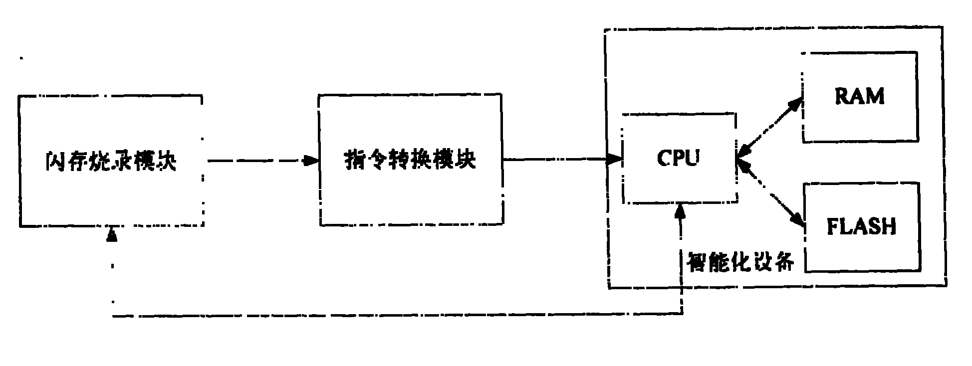
图1本发明智能化设备软件升级与修复系统的一个实施例的结构示意图。Fig. 1 is a schematic structural diagram of an embodiment of the intelligent equipment software upgrading and repairing system of the present invention.
具体实施方式 Detailed ways
下面结合附图及具体实施例对本发明进行详细说明。The present invention will be described in detail below in conjunction with the accompanying drawings and specific embodiments.
如图1所示,智能化设备软件升级与修复系统包括闪存烧录模块、指令转换模块和智能化设备(例如手机、个人数字助理PDA等)。As shown in Figure 1, the intelligent device software upgrade and repair system includes a flash memory programming module, an instruction conversion module and intelligent devices (such as mobile phones, personal digital assistants, PDAs, etc.).
闪存烧录模块,用于发出指令,通过指令转换模块,转换成标准的JTAG命令,使智能化设备的CPU进入Debug状态,经JTAG扫描链将智能化设备与闪存烧录模块接口驱动下载入智能化设备RAM指定区域,经JTAG扫描链将烧录软件所需插件,写入智能化设备RAM指定区域,经JTAG扫描链将程序计数器PC指针指向所述的RAM起始地址,然后退出Debug状态,运行写入RAM的接口驱动和烧录软件所需插件;该模块还用于与智能化设备直接通讯,发送需要下载的软件代码给智能化设备,写入到智能化设备的Flash中,完成下载;所述闪存烧录模块包含在PC机中。The flash memory programming module is used to issue commands, which are converted into standard JTAG commands through the command conversion module, so that the CPU of the intelligent device enters the Debug state, and the interface driver between the intelligent device and the flash memory programming module is downloaded into the smart device through the JTAG scan chain. In the designated area of the RAM of the intelligent device, the plug-in required for burning the software is written into the designated area of the RAM of the intelligent device through the JTAG scan chain, and the program counter PC pointer is pointed to the starting address of the RAM through the JTAG scan chain, and then exits the Debug state. Run the interface driver written in RAM and the plug-in required for burning software; this module is also used to communicate directly with the intelligent device, send the software code that needs to be downloaded to the intelligent device, write it into the Flash of the intelligent device, and complete the download ; The flash memory programming module is included in the PC.
指令转换模块,用于接收闪存烧录模块发送的指令,并将该指令转换成相应的JTAG命令,发送给智能化设备;所述指令转换模块与智能化设备通过JTAG接口通讯;所述指令转换模块可以包含在PC机中,也可以是一个独立的模块;若是一个独立的模块,则可以通过USB、串口、并口与PC机相连。The instruction conversion module is used to receive the instruction sent by the flash memory programming module, and convert the instruction into a corresponding JTAG command and send it to the intelligent device; the instruction conversion module communicates with the intelligent device through the JTAG interface; the instruction conversion The module can be included in the PC, or it can be an independent module; if it is an independent module, it can be connected to the PC through USB, serial port, and parallel port.
智能化设备,包括CPU,Flash,RAM,其中CPU是具有JTAG接口的芯片,用于与闪存烧录模块和指令转换模块通讯,并控制Flash和RAM;Flash用于存储智能化设备软件;RAM用于运行智能化设备软件。Intelligent equipment, including CPU, Flash, RAM, where CPU is a chip with JTAG interface, used to communicate with flash memory programming module and command conversion module, and control Flash and RAM; Flash is used to store intelligent equipment software; RAM is used to for running intelligent device software.
本发明智能化设备软件升级与修复的方法包括如下步骤:The method for upgrading and repairing intelligent equipment software of the present invention comprises the following steps:
步骤1,闪存烧录模块发出指令,通过指令转换模块,转换成标准的JTAG命令,使智能化设备的CPU进入调试Debug状态;智能化设备的CPU进入Debug状态后,可由JTAG扫描链将指令插入CPU流水线,从而控制CPU;Step 1, the flash memory programming module sends out instructions, which are converted into standard JTAG commands through the instruction conversion module, so that the CPU of the intelligent device enters the Debug state; after the CPU of the intelligent device enters the Debug state, the instruction can be inserted by the JTAG scan chain CPU pipeline to control CPU;
步骤2,闪存烧录模块通过指令转换模块初始化智能化设备的Flash、RAM以及CPU与Flash,RAM相关的寄存器。本步是通过JTAG指令模拟智能化设备软件的初始化程序达到的。首先通过JTAG扫描链直接访问智能化设备CPU相应的寄存器,修改为与所用FLASH和RAM所要求一致的值;然后通过JTAG扫描链将初始化Flash以及RAM的指令送到CPU的指令流水线,然后通过JTAG扫描链操作CPU执行流水线的指令,从而完成RAM与Flash的初始化。Step 2, the flash memory programming module initializes the Flash, RAM of the intelligent device, and registers related to the CPU, Flash, and RAM through the command conversion module. This step is achieved by simulating the initialization program of the intelligent device software through the JTAG command. First, directly access the corresponding register of the intelligent device CPU through the JTAG scan chain, and modify it to a value consistent with the requirements of the used FLASH and RAM; The scan chain operates the CPU to execute pipeline instructions to complete the initialization of RAM and Flash.
步骤3,闪存烧录模块通过指令转换模块,经JTAG扫描链将智能化设备与闪存烧录模块接口驱动即插件A下载入智能化设备RAM特定区域。这部分有两种做法:一种是通过JTAG扫描链路直接访问所需要存放代码的RAM区域,将接口驱动写入;另一种是通过JTAG扫描链把RAM存储数据的指令放在智能化设备CPU的指令流水线上,通过操控CPU运行RAM写入指令把所需程序写入。该插件的作用是使智能化设备可以与直接与PC机建立连接。Step 3, the flash memory programming module downloads the interface drive between the intelligent device and the flash memory programming module, that is, the plug-in A, into a specific area of the intelligent device RAM through the JTAG scan chain through the command conversion module. There are two methods for this part: one is to directly access the RAM area where the code needs to be stored through the JTAG scan link, and write the interface driver; the other is to place the instructions for storing data in RAM in the intelligent device through the JTAG scan link On the instruction pipeline of the CPU, the required program is written by manipulating the CPU to execute the RAM write instruction. The function of this plug-in is to enable the intelligent device to establish a connection with the PC directly.
步骤4,闪存烧录模块通过指令转换模块,经JTAG扫描链将烧录软件所需插件,即插件B写入智能化设备RAM特定区域,这个过程与第三步相同,也可以使用两种做法:一种是通过JTAG扫描链路直接访问所需要存放代码的RAM区域,将插件B写入;另一种是通过JTAG扫描链把RAM存储数据的指令放在智能化设备CPU的指令流水线上,通过操控CPU运行RAM写入指令把所需程序写入。该插件的作用是:建立智能化设备与闪存烧录模块的联系。这样,就可以直接通过闪存烧录模块与智能化设备接口取得所需数据,并通过智能化设备的CPU将之写入Flash存储器。Step 4, the flash memory programming module writes the plug-in required by the programming software, that is, plug-in B, into a specific area of the intelligent device RAM through the command conversion module and the JTAG scan chain. This process is the same as the third step, and two methods can also be used : One is to directly access the RAM area where the code needs to be stored through the JTAG scanning link, and write plug-in B; the other is to place the instruction for storing data in RAM on the instruction pipeline of the intelligent device CPU through the JTAG scanning link. Write the required program by manipulating the CPU to run the RAM write command. The function of this plug-in is to establish the connection between the intelligent device and the flash memory programming module. In this way, the required data can be directly obtained through the interface between the flash memory programming module and the intelligent device, and written into the Flash memory through the CPU of the intelligent device.
步骤5,闪存烧录模块通过指令转换模块,经JTAG扫描链将程序计数器PC指针指向第3和4步所述的RAM起始地址,然后退出Debug状态,运行插入RAM的插件。这个步骤通过JTAG扫描链修改CPU的PC寄存器,将PC指针指向上两步所讲的RAM起始地址,然后退出CPU Debug状态,CPU就会从PC指针开始依次运行每条指令。第3步的代码尾地址与第4步的代码起始地址应该相同,从而保证软件的顺序执行。插件A执行后,智能化设备便可以通过接口与PC机相连接;插件B执行后,智能化设备系统状态便处于软件下载状态。Step 5, the flash programming module uses the instruction conversion module to point the program counter PC pointer to the RAM start address described in steps 3 and 4 through the JTAG scan chain, then exits the Debug state, and runs the plug-in inserted into the RAM. This step modifies the PC register of the CPU through the JTAG scan chain, points the PC pointer to the RAM start address mentioned in the previous two steps, and then exits the CPU Debug state, and the CPU will run each instruction sequentially from the PC pointer. The code tail address in step 3 should be the same as the code start address in step 4, so as to ensure the sequential execution of the software. After the execution of plug-in A, the intelligent device can be connected to the PC through the interface; after the execution of plug-in B, the system status of the intelligent device is in the state of software download.
步骤6,闪存烧录模块与智能化设备直接通讯,智能化设备接收闪存烧录模块发送的软件代码,写入到Flash中,完成下载。Step 6, the flash memory programming module communicates directly with the intelligent device, and the intelligent device receives the software code sent by the flash memory programming module, writes it into the Flash, and completes the download.
本发明成本较低,最大的花销为指令转换模块,可以是硬件,也可以是软件。区别只是效率问题。通过第3步与第4步的插件A与B的写入,可以大大提高后续软件的烧录效率。原因如下:正常的软件升级或下载过程中,PC侧烧录软件与智能化设备通过接口相连,然后PC侧软件通过给智能化设备发送命令使之进入下载状态,此时智能化设备运行在下载模式,(相当于上面运行了插件1与插件2后的状态。)可以通过硬件接口从PC侧软件获取升级的代码,并写入Flash,完成升级。这个过程取决于Flash的写入速度。而智能化设备软件损坏的状态下,PC侧软件无法由正常途径控制智能化设备进入下载模式。所以现在市面上的专用烧录设备都是通过JTAG扫描链直接把数据写入Flash完成软件修复,这样速度取决于JTAG扫描链速度,当软件规模变得越来越大,这个修复时间便变得不可接受了。本文首先使用常用的JTAG扫描链技术初始化智能化设备RAM、Flash,为智能化设备进入正常的下载模式做准备;然后把智能化设备要进入正常的下载模式所需要的接口驱动、Flash擦写驱动以及智能化设备与PC侧软件相通讯的软件写入并运行,使的待维修智能化设备进入下载状态,然后快速完成软件向Flash写入。The cost of the present invention is relatively low, and the biggest expense is the instruction conversion module, which can be hardware or software. The difference is just a matter of efficiency. By writing plug-ins A and B in steps 3 and 4, the burning efficiency of subsequent software can be greatly improved. The reasons are as follows: During the normal software upgrade or download process, the programming software on the PC side is connected to the intelligent device through the interface, and then the software on the PC side sends a command to the intelligent device to enter the downloading state. mode, (equivalent to the state after running plug-in 1 and plug-in 2 above.) The upgrade code can be obtained from the PC side software through the hardware interface, and written into Flash to complete the upgrade. This process depends on the writing speed of Flash. However, when the software of the intelligent device is damaged, the software on the PC side cannot control the intelligent device to enter the download mode through normal means. Therefore, the dedicated programming devices on the market now directly write data into Flash through the JTAG scan chain to complete the software repair. This speed depends on the speed of the JTAG scan chain. When the software scale becomes larger and larger, the repair time becomes smaller. unacceptable. This article first uses the commonly used JTAG scan chain technology to initialize the intelligent device RAM and Flash, and prepares for the intelligent device to enter the normal download mode; And the software that communicates between the intelligent device and the PC side software is written and run, so that the intelligent device to be repaired enters the download state, and then quickly completes the writing of the software to the Flash.
本实施例的速度由两部分决定,一部分是第2~4步通过JTAG写入代码、修改CPU寄存器,速度较慢;第二部分是通过插件与PC侧闪存烧录模块交互数据,并完成Flash擦写,速度较快。第一部分软件代码量与第二部分比较非常小,随着智能化设备代码量的增加,第一部分所占比例会不断降低,从而与目前用专用烧录器直接通过JTAG扫描链把代码写入Flash比较,速度优势会愈加明显。本发明不需要专用烧录器的代码调试功能,实现容易,成本大大降低,在智能化设备生产维修中有很大优势。The speed of this embodiment is determined by two parts. One part is to write codes and modify CPU registers through JTAG in steps 2 to 4. The speed is relatively slow; Erase and write, the speed is faster. The amount of software code in the first part is very small compared with the second part. With the increase of the code amount of intelligent equipment, the proportion of the first part will continue to decrease, so it is different from the current use of a dedicated programmer to directly write the code into Flash through the JTAG scan chain. In comparison, the speed advantage will become more obvious. The invention does not need the code debugging function of a special burner, is easy to realize, and greatly reduces the cost, and has great advantages in the production and maintenance of intelligent equipment.
Claims (10)
Priority Applications (1)
| Application Number | Priority Date | Filing Date | Title |
|---|---|---|---|
| CNB2007100028365A CN100461105C (en) | 2007-02-01 | 2007-02-01 | Method and system for upgrading and repairing software of intelligent equipment |
Applications Claiming Priority (1)
| Application Number | Priority Date | Filing Date | Title |
|---|---|---|---|
| CNB2007100028365A CN100461105C (en) | 2007-02-01 | 2007-02-01 | Method and system for upgrading and repairing software of intelligent equipment |
Publications (2)
| Publication Number | Publication Date |
|---|---|
| CN101008898A CN101008898A (en) | 2007-08-01 |
| CN100461105C true CN100461105C (en) | 2009-02-11 |
Family
ID=38697342
Family Applications (1)
| Application Number | Title | Priority Date | Filing Date |
|---|---|---|---|
| CNB2007100028365A Expired - Fee Related CN100461105C (en) | 2007-02-01 | 2007-02-01 | Method and system for upgrading and repairing software of intelligent equipment |
Country Status (1)
| Country | Link |
|---|---|
| CN (1) | CN100461105C (en) |
Families Citing this family (13)
| Publication number | Priority date | Publication date | Assignee | Title |
|---|---|---|---|---|
| CN101110035B (en) * | 2007-08-20 | 2010-04-14 | 中兴通讯股份有限公司 | Program downloading method for terminal with JTAG interface |
| CN101350990B (en) * | 2008-08-20 | 2011-06-15 | 上海闻泰电子科技有限公司 | Method for updating CP of intelligent mobile phone |
| CN101500336B (en) * | 2009-03-12 | 2011-07-13 | 中兴通讯股份有限公司 | Mobile communication terminal and data download processing method thereof |
| CN101604249B (en) * | 2009-03-30 | 2013-01-23 | 华为技术有限公司 | Method for loading non-volatile memory program, embedded system and control device |
| CN102541576A (en) * | 2010-12-15 | 2012-07-04 | 沈阳新邮通信设备有限公司 | System repairing/updating method by adopting mode of mobile phone to mobile phone |
| CN102271190A (en) * | 2011-08-29 | 2011-12-07 | 惠州Tcl移动通信有限公司 | Mobile phone and downloading method thereof |
| CN103034507A (en) * | 2011-10-09 | 2013-04-10 | 上海共联通信信息发展有限公司 | Chip program repair method of telephone stored program control exchange |
| US9075686B2 (en) * | 2013-02-25 | 2015-07-07 | GM Global Technology Operations LLC | System and method to improve control module reflash time |
| CN104102499A (en) * | 2013-04-02 | 2014-10-15 | 中兴通讯股份有限公司 | Mobile terminal and mobile terminal software upgrading method |
| CN104158657A (en) * | 2014-07-16 | 2014-11-19 | 中兴通讯股份有限公司 | Information processing method and device, as well as encryption equipment |
| CN105138348A (en) * | 2015-07-23 | 2015-12-09 | 柳州龙辉科技有限公司 | Automatic update method for intelligent terminal software |
| CN114924757B (en) * | 2022-06-10 | 2023-03-28 | 北京东土科技股份有限公司 | Firmware burning-in method, device, control unit, system and storage medium |
| CN116185527A (en) * | 2023-03-08 | 2023-05-30 | 广州万协通信息技术有限公司 | Downloading method, device, equipment and storage medium of chip loading program |
Citations (4)
| Publication number | Priority date | Publication date | Assignee | Title |
|---|---|---|---|---|
| US20020162098A1 (en) * | 2001-03-19 | 2002-10-31 | Takuya Suzuki | Firmware writing system |
| CN1518252A (en) * | 2003-01-27 | 2004-08-04 | 华为技术有限公司 | Method and system for loading or upgrading logic devices |
| CN1858706A (en) * | 2006-04-12 | 2006-11-08 | 华为技术有限公司 | Method and system for 51 one-chip computer on-system upgrading |
| CN1858723A (en) * | 2006-01-24 | 2006-11-08 | 华为技术有限公司 | JIAG linkage method and device for using said method |
-
2007
- 2007-02-01 CN CNB2007100028365A patent/CN100461105C/en not_active Expired - Fee Related
Patent Citations (4)
| Publication number | Priority date | Publication date | Assignee | Title |
|---|---|---|---|---|
| US20020162098A1 (en) * | 2001-03-19 | 2002-10-31 | Takuya Suzuki | Firmware writing system |
| CN1518252A (en) * | 2003-01-27 | 2004-08-04 | 华为技术有限公司 | Method and system for loading or upgrading logic devices |
| CN1858723A (en) * | 2006-01-24 | 2006-11-08 | 华为技术有限公司 | JIAG linkage method and device for using said method |
| CN1858706A (en) * | 2006-04-12 | 2006-11-08 | 华为技术有限公司 | Method and system for 51 one-chip computer on-system upgrading |
Also Published As
| Publication number | Publication date |
|---|---|
| CN101008898A (en) | 2007-08-01 |
Similar Documents
| Publication | Publication Date | Title |
|---|---|---|
| CN100461105C (en) | Method and system for upgrading and repairing software of intelligent equipment | |
| CN102902556B (en) | The multistage boot load method of a kind of embedded equipment | |
| CN113900693B (en) | Firmware upgrading method, device and system, electronic equipment and storage medium | |
| CN103677915B (en) | A method of card is started based on TF and carries out the automatic programming of flash mirror | |
| CN104407878B (en) | C6000 digital signal processor online upgrading methods | |
| CN102360569B (en) | Burning method, system and apparatus for nand flash chips | |
| CN104133705B (en) | A kind of serial ports loads the system and method for PowerPC System guides files | |
| CN109669729A (en) | A kind of starting bootstrap technique of processor | |
| CN103677885A (en) | ARM FLASH simple program programming method | |
| US9836417B2 (en) | Bridge configuration in computing devices | |
| CN106909480B (en) | A kind of embedded system cross debugging method and device | |
| CN112148319A (en) | Parallel working FPGA (field programmable Gate array) online configuration system and method based on high-speed serial port | |
| CN108694052B (en) | Firmware upgrading method, firmware upgrading device and firmware upgrading system | |
| CN107704285A (en) | Field programmable gate array multi-version configuration chip, system and method | |
| CN110196726B (en) | A Method for Remotely Upgrading and Loading FPGA Programs Based on CPU+CPLD | |
| CN101159957A (en) | Method and device for upgrading and repairing data terminal equipment | |
| CN100383737C (en) | Method and system for online loading and upgrading of single-chip microcomputer | |
| CN113360440B (en) | Processor communication control method and related products | |
| CN104035757A (en) | MIPS-based (microprocessor without interlocked piped stages-based) U-boot (universal boot loader) transplantation implementing method | |
| CN117457054A (en) | Efuse control method, controller, electronic device and storage medium | |
| CN115495136B (en) | BMC quick online upgrading method based on domestic Feiteng platform | |
| CN108182079A (en) | A kind of TMS320C6748 program loading methods based on serial ports | |
| CN101753672B (en) | System and method for rapidly repairing wireless terminal | |
| CN100498708C (en) | Firmware download method and device using personal computer | |
| CN109426511B (en) | Soft core updating method and system |
Legal Events
| Date | Code | Title | Description |
|---|---|---|---|
| C06 | Publication | ||
| PB01 | Publication | ||
| C10 | Entry into substantive examination | ||
| SE01 | Entry into force of request for substantive examination | ||
| C14 | Grant of patent or utility model | ||
| GR01 | Patent grant | ||
| CF01 | Termination of patent right due to non-payment of annual fee | ||
| CF01 | Termination of patent right due to non-payment of annual fee |
Granted publication date: 20090211 Termination date: 20210201 |