CN100449764C - Photodetector - Google Patents
Photodetector Download PDFInfo
- Publication number
- CN100449764C CN100449764C CNB2004100908893A CN200410090889A CN100449764C CN 100449764 C CN100449764 C CN 100449764C CN B2004100908893 A CNB2004100908893 A CN B2004100908893A CN 200410090889 A CN200410090889 A CN 200410090889A CN 100449764 C CN100449764 C CN 100449764C
- Authority
- CN
- China
- Prior art keywords
- light
- filter layer
- wavelength
- photosensitive
- photoelectric conversion
- Prior art date
- Legal status (The legal status is an assumption and is not a legal conclusion. Google has not performed a legal analysis and makes no representation as to the accuracy of the status listed.)
- Expired - Lifetime
Links
Images


Classifications
-
- H—ELECTRICITY
- H10—SEMICONDUCTOR DEVICES; ELECTRIC SOLID-STATE DEVICES NOT OTHERWISE PROVIDED FOR
- H10F—INORGANIC SEMICONDUCTOR DEVICES SENSITIVE TO INFRARED RADIATION, LIGHT, ELECTROMAGNETIC RADIATION OF SHORTER WAVELENGTH OR CORPUSCULAR RADIATION
- H10F77/00—Constructional details of devices covered by this subclass
- H10F77/40—Optical elements or arrangements
-
- H—ELECTRICITY
- H10—SEMICONDUCTOR DEVICES; ELECTRIC SOLID-STATE DEVICES NOT OTHERWISE PROVIDED FOR
- H10F—INORGANIC SEMICONDUCTOR DEVICES SENSITIVE TO INFRARED RADIATION, LIGHT, ELECTROMAGNETIC RADIATION OF SHORTER WAVELENGTH OR CORPUSCULAR RADIATION
- H10F39/00—Integrated devices, or assemblies of multiple devices, comprising at least one element covered by group H10F30/00, e.g. radiation detectors comprising photodiode arrays
- H10F39/011—Manufacture or treatment of image sensors covered by group H10F39/12
- H10F39/024—Manufacture or treatment of image sensors covered by group H10F39/12 of coatings or optical elements
-
- H—ELECTRICITY
- H10—SEMICONDUCTOR DEVICES; ELECTRIC SOLID-STATE DEVICES NOT OTHERWISE PROVIDED FOR
- H10F—INORGANIC SEMICONDUCTOR DEVICES SENSITIVE TO INFRARED RADIATION, LIGHT, ELECTROMAGNETIC RADIATION OF SHORTER WAVELENGTH OR CORPUSCULAR RADIATION
- H10F39/00—Integrated devices, or assemblies of multiple devices, comprising at least one element covered by group H10F30/00, e.g. radiation detectors comprising photodiode arrays
- H10F39/80—Constructional details of image sensors
- H10F39/805—Coatings
- H10F39/8053—Colour filters
-
- H—ELECTRICITY
- H10—SEMICONDUCTOR DEVICES; ELECTRIC SOLID-STATE DEVICES NOT OTHERWISE PROVIDED FOR
- H10F—INORGANIC SEMICONDUCTOR DEVICES SENSITIVE TO INFRARED RADIATION, LIGHT, ELECTROMAGNETIC RADIATION OF SHORTER WAVELENGTH OR CORPUSCULAR RADIATION
- H10F39/00—Integrated devices, or assemblies of multiple devices, comprising at least one element covered by group H10F30/00, e.g. radiation detectors comprising photodiode arrays
- H10F39/80—Constructional details of image sensors
- H10F39/805—Coatings
- H10F39/8057—Optical shielding
-
- H—ELECTRICITY
- H10—SEMICONDUCTOR DEVICES; ELECTRIC SOLID-STATE DEVICES NOT OTHERWISE PROVIDED FOR
- H10F—INORGANIC SEMICONDUCTOR DEVICES SENSITIVE TO INFRARED RADIATION, LIGHT, ELECTROMAGNETIC RADIATION OF SHORTER WAVELENGTH OR CORPUSCULAR RADIATION
- H10F39/00—Integrated devices, or assemblies of multiple devices, comprising at least one element covered by group H10F30/00, e.g. radiation detectors comprising photodiode arrays
- H10F39/80—Constructional details of image sensors
- H10F39/806—Optical elements or arrangements associated with the image sensors
- H10F39/8063—Microlenses
-
- H—ELECTRICITY
- H10—SEMICONDUCTOR DEVICES; ELECTRIC SOLID-STATE DEVICES NOT OTHERWISE PROVIDED FOR
- H10F—INORGANIC SEMICONDUCTOR DEVICES SENSITIVE TO INFRARED RADIATION, LIGHT, ELECTROMAGNETIC RADIATION OF SHORTER WAVELENGTH OR CORPUSCULAR RADIATION
- H10F77/00—Constructional details of devices covered by this subclass
- H10F77/40—Optical elements or arrangements
- H10F77/413—Optical elements or arrangements directly associated or integrated with the devices, e.g. back reflectors
Landscapes
- Solid State Image Pick-Up Elements (AREA)
- Light Receiving Elements (AREA)
Abstract
一种光电探测器,包括具有光敏单元(1a,1b,1c)的半导体衬底。每个光敏单元设有,透射光敏单元预定波长范围内光的滤光层20,和光电转换单元17,可操作用于根据透射通过滤光层20的光的强度产生信号电荷。滤光层20的厚度(ta,tb,tc)相应于各个光敏单元预定的波长范围。通过这种结构,可以提供成本有效的光电探测器,其在制造滤色片时,可以不需要对不同颜色的颜料和染料的材料进行管理。
A photodetector comprising a semiconductor substrate with a photosensitive unit (1a, 1b, 1c). Each photosensitive cell is provided with a filter layer 20 that transmits light within a predetermined wavelength range of the photosensitive cell, and a photoelectric conversion unit 17 operable to generate signal charges according to the intensity of light transmitted through the filter layer 20 . The thickness (ta, tb, tc) of the filter layer 20 corresponds to the predetermined wavelength range of the respective photosensitive unit. With this structure, it is possible to provide a cost-effective photodetector that does not require material management of pigments and dyes of different colors when manufacturing a color filter.
Description
技术领域 technical field
本发明涉及光电探测器如图像传感器等,更具体地涉及光电探测器的光敏单元中设置的彩色滤光片。The present invention relates to a photodetector such as an image sensor, and more particularly to a color filter arranged in a photosensitive unit of the photodetector.
背景技术 Background technique
通常使用的光电探测器包括具有多个光敏单元的半导体衬底衬底,每个光敏单元设有滤色片和光电二极管。在光电探测器中存在红色滤色片(R),绿色滤色片(G),和蓝色滤色片(B),每个光敏单元中分配有三种颜色之一的滤色片。光电二极管响应通过滤色片的光的强度产生信号电荷。因此,每个光敏单元中产生响应入射光中特定颜色的光的信号电荷。通过收集在光敏单元中产生的三种颜色的信号电荷而产生图像的成像数据(例如参见日本公开专利申请No.H05-006986)。A commonly used photodetector includes a semiconductor substrate with a plurality of photosensitive units, each photosensitive unit is provided with a color filter and a photodiode. There are red color filters (R), green color filters (G), and blue color filters (B) in the photodetector, and a color filter of one of the three colors is assigned to each photosensitive unit. The photodiode generates a signal charge in response to the intensity of light passing through the color filter. Thus, signal charges are generated in each photosensitive cell in response to light of a particular color in the incident light. Imaging data of an image is generated by collecting signal charges of three colors generated in a photosensitive cell (see, for example, Japanese Laid-Open Patent Application No. H05-006986).
常规滤色片通常通过将丙烯酸树脂混合各自相应颜色的颜料或染料来制造(例如见日本公开专利申请No.H07-311310)。Conventional color filters are generally produced by mixing acrylic resins with pigments or dyes of respective colors (see, for example, Japanese Laid-Open Patent Application No. H07-311310).
然而,制造常规的滤色片在制造过程中对于不同颜色的颜料或染料需要进行烦琐的材料管理,这妨碍了光电探测器的成本降低。However, manufacturing a conventional color filter requires cumbersome material management for different colors of pigments or dyes during the manufacturing process, which prevents cost reduction of photodetectors.
发明内容 Contents of the invention
鉴于上述问题,本发明的目的在于提供低成本高效益的光电探测器,其在制造过程中不需要对颜料或染料进行材料管理。In view of the above problems, it is an object of the present invention to provide a cost-effective photodetector that does not require material management of pigments or dyes during the manufacturing process.
为了实现上述目的,本发明的光电探测器包括具有多个光敏单元的半导体衬底,每个光敏单元包括:滤光层,透射光敏单元预定波长范围内的光;和光电转换单元,可操作用于根据透射光的强度产生信号电荷,其中每一滤光层的厚度相应于每个光敏单元预定的波长范围,并且所有光敏单元中的每一滤光层都仅由一种材料制成。In order to achieve the above object, the photodetector of the present invention includes a semiconductor substrate having a plurality of photosensitive units, each photosensitive unit comprising: a filter layer for transmitting light within a predetermined wavelength range of the photosensitive unit; and a photoelectric conversion unit operable for Signal charges are generated according to the intensity of transmitted light, wherein the thickness of each filter layer corresponds to the predetermined wavelength range of each photosensitive unit, and each filter layer in all photosensitive units is made of only one material.
利用上述结构,以每一滤光层相应于预定颜色的厚度为基础,确定透射通过滤光层的光的波长范围。因此,不同颜色的颜料或染料的材料管理在制造过程中不是必要的,从而生产成本可以降低。With the above structure, the wavelength range of light transmitted through the filter layers is determined on the basis of the thickness of each filter layer corresponding to a predetermined color. Therefore, material management of pigments or dyes of different colors is not necessary in the manufacturing process, so that the production cost can be reduced.
上述光电探测器也可以为这种结构,其中滤光层仅由一种材料制成,该材料在光波长小于截止波长时的透射率低于光波长等于或大于截止波长时的透射率,截止波长由该材料的厚度确定。The above-mentioned photodetector may also be of such a structure, wherein the filter layer is made of only one material whose transmittance is lower than the transmittance when the light wavelength is equal to or greater than the cut-off wavelength, and the cut-off The wavelength is determined by the thickness of the material.
利用上述结构,可以使滤光层具有主要透射波长大于截止波长的光的滤色片的功能。With the above structure, the filter layer can have the function of a color filter that mainly transmits light with a wavelength greater than the cutoff wavelength.
上述光电探测器也可以是这种结构,其中滤光层由透射率通过吸收光而降低的材料制成。The above-mentioned photodetector may also be a structure in which the filter layer is made of a material whose transmittance is reduced by absorbing light.
为了减少光透射,存在两种可能的方法。一种为使滤光层吸收光,另一种为使滤光层反射光。在后面一种方法中,由滤光层反射的光可以在光电探测器中散射,因此眩光(flare)现象的发生高于前面一种方法的情况。眩光为这样一种现象,即正确的信号与从邻近光敏单元中反射的光的不正确信号重叠。利用本发明,眩光现象的发生率通过使用前面一种方法而得到减小。In order to reduce light transmission, there are two possible approaches. One is to make the filter layer absorb light, and the other is to make the filter layer reflect light. In the latter method, the light reflected by the filter layer may be scattered in the photodetector, so the occurrence of the flare phenomenon is higher than in the case of the former method. Glare is the phenomenon where a correct signal overlaps with an incorrect signal of light reflected from adjacent photosensitive cells. With the present invention, the occurrence rate of the glare phenomenon is reduced by using the former method.
上述光电探测器也可以是这种结构,其中滤光层由多晶硅、非晶硅、和硅中的一种构成。The aforementioned photodetector may also have a structure in which the filter layer is made of one of polysilicon, amorphous silicon, and silicon.
利用上述结构,滤光层可以利用半导体制造技术来制造。例如,利用CVD技术在光敏单元上形成多晶硅层,然后进行干蚀刻使每一层具有为每个光敏单元预定的厚度。With the above structure, the filter layer can be manufactured using semiconductor manufacturing technology. For example, a polysilicon layer is formed on the photosensitive unit using CVD technology, and then dry-etched so that each layer has a predetermined thickness for each photosensitive unit.
因此,处理丙烯酸树脂的滤色片制造过程是不需要的。而且,可以利用半导体制造的制造设备以及简化制造过程。Therefore, a color filter manufacturing process dealing with acrylic resin is unnecessary. Also, it is possible to utilize manufacturing equipment for semiconductor manufacturing and simplify the manufacturing process.
上述光电探测器也可以是这种结构,其中衬底由硅制成,光电转换单元通过在衬底中掺杂N型杂质形成,滤光层通过在光电转换单元中掺杂P型杂质形成。The aforementioned photodetector may also have this structure, wherein the substrate is made of silicon, the photoelectric conversion unit is formed by doping the substrate with N-type impurities, and the filter layer is formed by doping the photoelectric conversion unit with P-type impurities.
利用上述结构,滤光层可以利用半导体制造技术来制造。例如,可以通过调整P型杂质的加速能量使滤光层具有每个光敏单元所需厚度。With the above structure, the filter layer can be manufactured using semiconductor manufacturing technology. For example, the filter layer can have the required thickness of each photosensitive unit by adjusting the acceleration energy of the P-type impurities.
因此,处理丙烯酸树脂的滤色片制造过程是不需要的。这样,可以利用半导体制造的制造设备以及简化制造过程。Therefore, a color filter manufacturing process dealing with acrylic resin is unnecessary. In this way, manufacturing equipment for semiconductor manufacturing can be utilized and the manufacturing process can be simplified.
上述光电探测器也可以是这种结构,其中滤光层由截止波长随着材料变厚而变大的材料制成。The above-mentioned photodetector may also have a structure in which the filter layer is made of a material whose cutoff wavelength becomes larger as the material becomes thicker.
利用上述结构,可以通过确定厚度,调整在所需波长范围内透射的光。With the above structure, it is possible to adjust the transmitted light in a desired wavelength range by determining the thickness.
上述光电探测器也可以是这种结构,其中每一滤光层的厚度为第一厚度、第二厚度和第三厚度之一,第一厚度的截止波长在红光波长范围和绿光波长范围之间,第二厚度的截止波长在绿光波长范围和蓝光波长范围之间,以及第三厚度的截止波长在蓝光波长范围和紫外波长范围之间。The above-mentioned photodetector can also have this structure, wherein the thickness of each filter layer is one of the first thickness, the second thickness and the third thickness, and the cut-off wavelength of the first thickness is in the red wavelength range and the green wavelength range Between, the cutoff wavelength of the second thickness is between the green wavelength range and the blue wavelength range, and the cutoff wavelength of the third thickness is between the blue wavelength range and the ultraviolet wavelength range.
根据上述结构,每个光敏单元中设置的每一滤光层可以根据滤光层的厚度透射下述波长范围之一内的光。According to the above structure, each filter layer provided in each photosensitive unit can transmit light in one of the following wavelength ranges according to the thickness of the filter layer.
第一厚度:红光波长范围First Thickness: Red Light Wavelength Range
第二厚度:红光和绿光波长范围Second thickness: red and green wavelength range
第三厚度:红光、绿光和蓝光波长范围Third Thickness: Red, Green, and Blue Wavelength Ranges
具体地,相应于红光波长范围内的光的信号电荷在第一光敏单元中产生,该第一光敏单元设有具有第一厚度的滤光层。相似地,相应于红光和绿光波长范围内的光的信号电荷在第二光敏单元中产生,该第二光敏单元设有具有第二厚度的滤光层,以及相应于红光、绿光和蓝光波长范围内的光的信号电荷在第三光敏单元中产生,该第三光敏单元设有具有第三厚度的滤光层。Specifically, signal charges corresponding to light in the red wavelength range are generated in the first photosensitive unit provided with a filter layer having a first thickness. Similarly, signal charges corresponding to light in the red and green wavelength ranges are generated in a second photosensitive unit provided with a filter layer having a second thickness, and corresponding to red, green Signal charges for light in the wavelength range of and blue light are generated in a third photosensitive unit provided with a filter layer having a third thickness.
从而,红色信号根据在第一光敏单元中产生的信号电荷得到。并且,绿色信号根据在第一和第二光敏单元中产生的信号电荷之间的差值得到。同样,蓝色信号根据在第二和第三光敏单元中产生的信号电荷之间的差值得到。Thus, a red signal is derived from the signal charge generated in the first photosensitive cell. And, a green signal is derived from a difference between signal charges generated in the first and second photosensitive cells. Likewise, the blue signal is derived from the difference between the signal charges generated in the second and third photosensitive cells.
上述光电探测器也可以是这种结构,其中光敏单元进一步包括抗反射层,其由折射率小于滤光层折射率的材料制成,抗反射层设置在滤光层面向光源的主表面上。The photodetector above can also be of this structure, wherein the photosensitive unit further includes an anti-reflection layer made of a material with a lower refractive index than the filter layer, and the anti-reflection layer is disposed on the main surface of the filter layer facing the light source.
利用上述结构,抗反射层配置在滤光层和气体之间,入射光的反射率可以减小。因此,可以提高光电探测器的灵敏度。With the above structure, the anti-reflection layer is disposed between the filter layer and the gas, and the reflectance of incident light can be reduced. Therefore, the sensitivity of the photodetector can be improved.
上述光电探测器也可以是这种结构,其中滤光层由多晶硅、非晶硅、和硅之一构成,抗反射层由氮化硅、二氧化硅、和氮氧化硅之一构成。The above-mentioned photodetector may also have this structure, wherein the filter layer is made of one of polysilicon, amorphous silicon, and silicon, and the antireflection layer is made of one of silicon nitride, silicon dioxide, and silicon oxynitride.
利用上述结构,滤光层和抗反射层可以利用半导体制造技术来制造。因此,利用半导体制造的制造设备以及简化制造过程是可能的。With the above structure, the filter layer and the anti-reflection layer can be manufactured using semiconductor manufacturing technology. Therefore, it is possible to utilize manufacturing equipment for semiconductor manufacturing and to simplify the manufacturing process.
上述光电探测器也可以是这种结构,其中光敏单元进一步包括光屏蔽形成层,其在相应于光电转换单元的部分具有遮光层和小孔,遮光层阻隔除通过小孔以外的光,滤光层位于光屏蔽形成层和光电转换单元之间。The above-mentioned photodetector may also be of such a structure, wherein the photosensitive unit further includes a light-shielding forming layer having a light-shielding layer and a small hole at a portion corresponding to the photoelectric conversion unit, the light-shielding layer blocks light other than passing through the small hole, and filters light. The layer is located between the light-shielding forming layer and the photoelectric conversion unit.
利用上述结构,可以防止相邻光敏单元散射的光进入光电转换单元。从而,在每个光敏单元中,由来自于相邻光敏单元的散射光引起的噪声减小。With the above structure, it is possible to prevent light scattered by adjacent photosensitive cells from entering the photoelectric conversion cells. Thus, in each photosensitive cell, noise caused by scattered light from neighboring photosensitive cells is reduced.
上述光电探测器也可以是这种结构,其中光敏单元进一步包括二氧化硅层,其厚度在1nm到150nm的范围内,设置在滤光层和光电转换单元之间。The aforementioned photodetector may also have this structure, wherein the photosensitive unit further includes a silicon dioxide layer with a thickness in the range of 1 nm to 150 nm, disposed between the filter layer and the photoelectric conversion unit.
利用上述结构,可以使滤光层和光电转换单元绝缘。这样,可以防止光电转换单元的信号电荷泄漏到滤光层。With the above structure, the filter layer and the photoelectric conversion unit can be insulated. In this way, the signal charge of the photoelectric conversion unit can be prevented from leaking to the filter layer.
通常,入射光在二氧化硅层和光电转换单元之间的边界面以一定反射率反射。然而,已知反射率可以通过将二氧化硅层的厚度设定在1nm到150nm的范围内减小。因此,可以通过插入二氧化硅层来抑制光敏单元灵敏度的降低。In general, incident light is reflected with a certain reflectance at the boundary surface between the silicon dioxide layer and the photoelectric conversion unit. However, it is known that the reflectance can be reduced by setting the thickness of the silicon dioxide layer within the range of 1 nm to 150 nm. Therefore, the decrease in the sensitivity of the photosensitive cell can be suppressed by interposing the silicon dioxide layer.
上述光电探测器也可以是这种结构,其中光敏单元进一步包括:栅极,当信号电荷没有输送时,可操作用于在光电转换单元和输送目标区之间的栅极区中产生栅极电势,栅极电势低于光电转换单元处的电势;和势垒,配置在滤光层和光电转换单元之间,在势垒处产生低于栅极电势的势垒电势。The photodetector described above may also be of a structure wherein the photosensitive unit further includes: a gate operable to generate a gate potential in a gate region between the photoelectric conversion unit and the transfer target region when the signal charge is not transferred , the gate potential is lower than the potential at the photoelectric conversion unit; and a potential barrier is disposed between the filter layer and the photoelectric conversion unit, and a potential barrier potential lower than the gate potential is generated at the potential barrier.
利用上述结构,在非输送时间内,栅极区域、光电转换单元、和势垒处的电势分别为低、高、和低。这样,光电转换单元中产生的电子积聚在具有较高电势的光电转换单元中。同样通过这种结构,可以防止积聚的电子越过势垒泄漏到滤光层。With the above structure, during the non-transfer time, the potentials at the gate region, the photoelectric conversion unit, and the potential barrier are low, high, and low, respectively. In this way, electrons generated in the photoelectric conversion unit are accumulated in the photoelectric conversion unit having a higher potential. Also with this structure, accumulated electrons can be prevented from leaking over the potential barrier to the filter layer.
进一步,为了实现上述目标,根据本发明的光电探测器包括具有多个光敏单元的半导体衬底,每个光敏单元包括:光电转换单元,可操作用于根据光强产生信号电荷,其中一些光敏单元每个都设有滤光层,通过滤光层向光电转换单元传输光,每一滤光层的厚度相应于每个光敏单元预定的波长范围,所有所述一些光敏单元中的每一滤光层都仅由一种材料制成,而剩余的光敏单元不设置滤光层。Further, in order to achieve the above object, the photodetector according to the present invention includes a semiconductor substrate having a plurality of photosensitive units, each photosensitive unit includes: a photoelectric conversion unit operable to generate signal charges according to light intensity, some of which photosensitive units Each is provided with a filter layer through which light is transmitted to the photoelectric conversion unit, the thickness of each filter layer corresponds to the predetermined wavelength range of each photosensitive unit, and each filter in all the photosensitive units The layers are all made of only one material, while the remaining photosensitive cells are not provided with filter layers.
利用上述结构,相似于之前描述的光电探测器,不同颜色的颜料或染料的材料管理在制造过程中是不必要的,从而生产成本可以降低。With the above structure, similar to the previously described photodetector, material management of pigments or dyes of different colors is unnecessary in the manufacturing process, so that the production cost can be reduced.
上述光电探测器也可以为这种结构,其中滤光层由一种材料制成,该材料对光波长小于截止波长的光的透射率低于对光波长等于或大于截止波长的光的透射率,截止波长由材料的厚度确定。The above-mentioned photodetector may also have a structure in which the filter layer is made of a material whose transmittance to light having a wavelength smaller than the cutoff wavelength is lower than the transmittance to light having a wavelength equal to or greater than the cutoff wavelength , the cutoff wavelength is determined by the thickness of the material.
利用上述结构,可以使滤光层具有主要透射波长大于截止波长的光的滤色片的功能。With the above structure, the filter layer can have the function of a color filter that mainly transmits light with a wavelength greater than the cutoff wavelength.
上述光电探测器也可以是这种结构,其中每一滤光层的厚度为第一厚度和第二厚度之一,第一厚度的截止波长在红光波长范围和绿光波长范围之间,第二厚度的截止波长在绿光波长范围和蓝光波长范围之间。The above-mentioned photodetector can also have this structure, wherein the thickness of each filter layer is one of the first thickness and the second thickness, the cut-off wavelength of the first thickness is between the red light wavelength range and the green light wavelength range, and the second thickness is between the red light wavelength range and the green light wavelength range. The cut-off wavelength of the second thickness is between the green light wavelength range and the blue light wavelength range.
这种结构可以应用于光电探测器接收紫外线已经被去除的光的情况。通常,在普通的成像系统中,在通过光学低通滤光片和红外截止滤光片后,由透镜聚集的入射光到达光电探测器。在这样的成像系统中,如果也设置了紫外截止滤光片,则紫外截止滤光片用作透射波长大于蓝光波长范围和紫外波长范围之间界限的波长范围的光。因此,基于该波长范围内的光产生信号电荷的光敏单元中不需要滤光层。This structure can be applied to the case where the photodetector receives light from which ultraviolet rays have been removed. Usually, in an ordinary imaging system, after passing through an optical low-pass filter and an infrared cut filter, the incident light collected by a lens reaches a photodetector. In such an imaging system, if a UV cut filter is also provided, the UV cut filter serves to transmit light of a wavelength range whose wavelength is greater than the boundary between the blue wavelength range and the UV wavelength range. Therefore, no filter layers are required in photosensitive cells that generate signal charges based on light in this wavelength range.
从而,可以缩短滤光层的制造过程,因为仅形成用于两种颜色的滤光层对于光电探测器已经足够,而不用形成三种颜色的滤光层,。Thus, the manufacturing process of the filter layers can be shortened because it is sufficient to form filter layers for only two colors for the photodetector without forming filter layers for three colors.
根据本发明的信号处理装置基于由如权利要求1所述的光电探测器产生的多个源信号中的第一源信号和第二源信号得到颜色信号,第一源信号相应于第一波长范围内的光强,第二源信号相应于包括第一波长范围的第二波长范围内的光强,颜色信号相应于排除第一波长范围的第二波长范围内的光强,信号处理装置包括:保持单元,保持分别相应于第一源信号和第二源信号的加权系数;和计算单元,可操作用于通过将第一源信号和第二源信号分别乘上加权系数,然后从相乘的结果之间导出差值,从而得到颜色信号。The signal processing device according to the present invention obtains a color signal based on a first source signal and a second source signal among a plurality of source signals produced by the photodetector as claimed in
利用上述结构,信号处理装置可以得到相应于排除第一波长范围的第二波长范围内光强的颜色信号。当光电探测器如上所述输出第一源信号和第二源信号时使用上述信号处理装置。With the above structure, the signal processing means can obtain a color signal corresponding to the light intensity in the second wavelength range excluding the first wavelength range. The above-described signal processing means is used when the photodetector outputs the first source signal and the second source signal as described above.
根据本发明的信号处理装置基于由如权利要求1所述的光电探测器产生的多个源信号中的第一源信号,第二源信号和第三源信号得到相应于红光波长范围内光强的红色信号,相应于绿光波长范围内光强的绿色信号,和相应于蓝光波长范围内光强的蓝色信号,第一源信号相应于波长范围大于红光波长范围和绿光波长范围之间的波长的光强,第二源信号相应于波长范围大于绿光波长范围和蓝光波长范围之间的波长的光强,第三源信号相应于波长范围大于蓝光波长范围和紫外波长范围之间的波长的光强,信号处理装置包括:保持单元,保持将一组第一源信号,第二源信号和第三源信号转换为一组红色信号,绿色信号和蓝色信号的转换矩阵;和计算单元,可操作用于将转换矩阵应用于该组第一源信号,第二源信号和第三源信号。According to the signal processing device of the present invention, the first source signal, the second source signal and the third source signal among the plurality of source signals generated by the photodetector according to
每个源信号相应于下述波长范围的光的强度。Each source signal corresponds to the intensity of light in the wavelength range described below.
第一源信号:红光波长范围First source signal: red light wavelength range
第二源信号:红光和绿光波长范围Second source signal: red and green wavelength range
第三源信号:红光、绿光和蓝光波长范围Third source signal: red, green and blue wavelength ranges
根据上述结构,信号处理装置可以根据该组第一源信号,第二源信号和第三源信号得到一组红色信号,绿色信号和蓝色信号,如下:According to the above structure, the signal processing device can obtain a group of red signals, green signals and blue signals according to the group of first source signals, second source signals and third source signals, as follows:
红色信号:红光波长范围Red signal: red light wavelength range
绿色信号:绿光波长范围Green signal: Green light wavelength range
蓝色信号:蓝光波长范围Blue signal: blue light wavelength range
根据本发明的一种制造光电探测器的方法,其中包括形成具有多个光敏单元的半导体衬底,每个光敏单元设有滤光层,其透射光敏单元预定波长范围内的光,和光电转换单元,可操作用于根据透射光的强度产生信号电荷,该方法包括:在每个光敏单元上形成光电转换单元;在每个光电转换单元上形成相同厚度的层,该层由一种材料制成,该材料的透射光的波长范围基于厚度确定;和通过蚀刻所述层在所有光敏单元中形成仅由一种材料制成的每一滤光层,以便得到的层具有根据每个光敏单元预定的厚度。A method of manufacturing a photodetector according to the present invention, which includes forming a semiconductor substrate with a plurality of photosensitive units, each photosensitive unit is provided with a filter layer that transmits light within a predetermined wavelength range of the photosensitive unit, and photoelectric conversion A unit operable to generate a signal charge according to the intensity of transmitted light, the method comprising: forming a photoelectric conversion unit on each photosensitive unit; forming a layer of the same thickness on each photosensitive unit, the layer being made of a material , the wavelength range of the transmitted light of the material is determined based on the thickness; and forming each filter layer made of only one material in all photosensitive units by etching said layer so that the resulting layer has predetermined thickness.
利用上述结构,通过滤光层透射的光的波长范围基于相应于预定颜色的每一层的厚度确定。因此,不同颜色的颜料或染料的材料管理在制造过程中不是必要的,从而生产成本可以降低。With the above structure, the wavelength range of light transmitted through the filter layer is determined based on the thickness of each layer corresponding to a predetermined color. Therefore, material management of pigments or dyes of different colors is not necessary in the manufacturing process, so that the production cost can be reduced.
进一步,如果选择多晶硅或非晶硅作为构成滤光层的材料,滤光层可以利用半导体制造技术来制造。因此,管理丙烯酸树脂的滤色片制造过程不是必要的。结果,可以利用半导体制造的制造设备以及简化制造过程。Further, if polysilicon or amorphous silicon is selected as the material constituting the filter layer, the filter layer can be manufactured using semiconductor manufacturing techniques. Therefore, it is not necessary to manage the color filter manufacturing process of acrylic resin. As a result, manufacturing equipment for semiconductor manufacturing can be utilized and the manufacturing process can be simplified.
根据本发明的一种制造光电探测器的方法,其中光电探测器包括具有多个光敏单元的半导体衬底,每个光敏单元设有透射光敏单元预定波长范围内的光的滤光层,和光电转换单元,可操作用于根据透射光的强度产生信号电荷,该方法包括:通过在每个光敏单元中掺杂N型杂质形成光电转换单元;以及通过在光电转换单元中掺杂P型杂质在所有光敏单元中形成仅由一种材料制成的每一滤光层,以使掺杂部分具有根据每个光敏单元预定的厚度。A method of manufacturing a photodetector according to the present invention, wherein the photodetector includes a semiconductor substrate having a plurality of photosensitive units, each photosensitive unit is provided with a filter layer that transmits light within a predetermined wavelength range of the photosensitive unit, and a photoelectric a conversion unit operable to generate signal charges according to the intensity of transmitted light, the method comprising: forming a photoelectric conversion unit by doping an N-type impurity in each photosensitive unit; and forming a photoelectric conversion unit by doping a P-type impurity in the photoelectric conversion unit Each filter layer made of only one material is formed in all photosensitive cells so that the impurity portion has a predetermined thickness according to each photosensitive cell.
利用上述结构,通过滤光层透射的光的波长范围基于相应于预定颜色的每一层厚度确定。因此,不同颜色的颜料或染料的材料管理在制造过程中是不必要的,从而生产成本可以降低。With the above structure, the wavelength range of light transmitted through the filter layer is determined based on the thickness of each layer corresponding to a predetermined color. Therefore, material management of pigments or dyes of different colors is unnecessary in the manufacturing process, so that the production cost can be reduced.
进一步,滤光层可以利用半导体制造技术来制造。因此,管理丙烯酸树脂的滤色片制造过程是不必要的。这样,可以利用半导体制造的制造设备以及简化制造过程。Further, the filter layer can be manufactured using semiconductor manufacturing technology. Therefore, it is unnecessary to manage the color filter manufacturing process of acrylic resin. In this way, manufacturing equipment for semiconductor manufacturing can be utilized and the manufacturing process can be simplified.
附图说明 Description of drawings
本发明的这些和其他目的、优点和特征将从下面结合所附附图的描述中明显得到,这些附图说明本发明的具体实施例。These and other objects, advantages and features of the invention will become apparent from the following description taken in conjunction with the accompanying drawings, which illustrate specific embodiments of the invention.
在附图中:In the attached picture:
图1说明了根据本发明的成像系统的结构;Figure 1 illustrates the structure of an imaging system according to the present invention;
图2为根据第一实施例的光敏单元(1a,1b,1c)的截面图;Figure 2 is a cross-sectional view of a photosensitive unit (1a, 1b, 1c) according to a first embodiment;
图3为示出了多晶硅层和红外截止滤光片的光透射率的曲线图;3 is a graph showing the light transmittance of a polysilicon layer and an infrared cut filter;
图4为说明了信号处理电路的内部结构的框图;FIG. 4 is a block diagram illustrating an internal structure of a signal processing circuit;
图5A-5B示出了保持在矩阵保持单元61中的矩阵和逆矩阵;5A-5B show the matrix and inverse matrix held in the
图6A-6H说明了制造滤光层20的方法的一个例子;6A-6H have illustrated an example of the method for manufacturing optical filter layer 20;
图7为根据第二实施例的光敏单元(1a,1b,1c)的截面图;Figure 7 is a cross-sectional view of a photosensitive unit (1a, 1b, 1c) according to a second embodiment;
图8为根据第三实施例的光敏单元(1a,1b,1c)的截面图;Figure 8 is a cross-sectional view of a photosensitive unit (1a, 1b, 1c) according to a third embodiment;
图9A和9B示出了光敏单元中滤光层20、势垒23、光电转换单元17和迁移晶体管24的电势;9A and 9B show the potentials of the filter layer 20, potential barrier 23,
图10为根据第四实施例的光敏单元(1a,1b,1c)的截面图;Figure 10 is a cross-sectional view of a photosensitive unit (1a, 1b, 1c) according to a fourth embodiment;
图11A-11C示出了电势与距离光敏单元中绝缘层13和光电二极管层12之间边界面的距离之间的联系;11A-11C show the relationship between the potential and the distance from the boundary surface between the insulating layer 13 and the
图12A-12G说明了制造滤光层20的方法的另一个例子;和12A-12G illustrate another example of the method for making the filter layer 20; and
图13为根据变形实施例的光敏单元(1a,1b,1c)的截面图。Fig. 13 is a cross-sectional view of a photosensitive unit (1a, 1b, 1c) according to a modified embodiment.
具体实施方式 Detailed ways
第一实施例first embodiment
[概要][summary]
在第一实施例中,所有像素单元中的滤光层仅由多晶硅构成。作为多晶硅的一个特性,通过多晶硅层透射的光的波长范围根据层的厚度变化。因此,通过设定每个光敏单元彼此不同的多晶硅层厚度,可以使用多晶硅滤光层作为滤色片。In the first embodiment, the filter layers in all pixel units are only made of polysilicon. As a characteristic of polysilicon, the wavelength range of light transmitted through a polysilicon layer varies according to the thickness of the layer. Therefore, by setting the thickness of the polysilicon layer different from each other for each photosensitive unit, the polysilicon filter layer can be used as a color filter.
由于通过多晶硅滤光层透射的光的波长范围基于相应的滤光层厚度而不是每个颜色的颜料或染料来确定,因此在制造滤光层的过程中不需要对不同颜色的颜料或染料进行材料控制。因此,生产成本可以降低。Since the wavelength range of light transmitted through the polysilicon filter layer is determined based on the thickness of the corresponding filter layer rather than each color of pigment or dye, there is no need for different color pigments or dyes in the process of manufacturing the filter layer. material control. Therefore, production costs can be reduced.
此外,滤光层可以利用半导体制造技术来制造,并且管理丙烯酸树脂的滤色片制造过程不是必要的。结果,可以利用半导体制造的制造设备以及简化制造过程。In addition, the filter layer can be manufactured using semiconductor manufacturing technology, and it is not necessary to manage the color filter manufacturing process of acrylic resin. As a result, manufacturing equipment for semiconductor manufacturing can be utilized and the manufacturing process can be simplified.
[结构][structure]
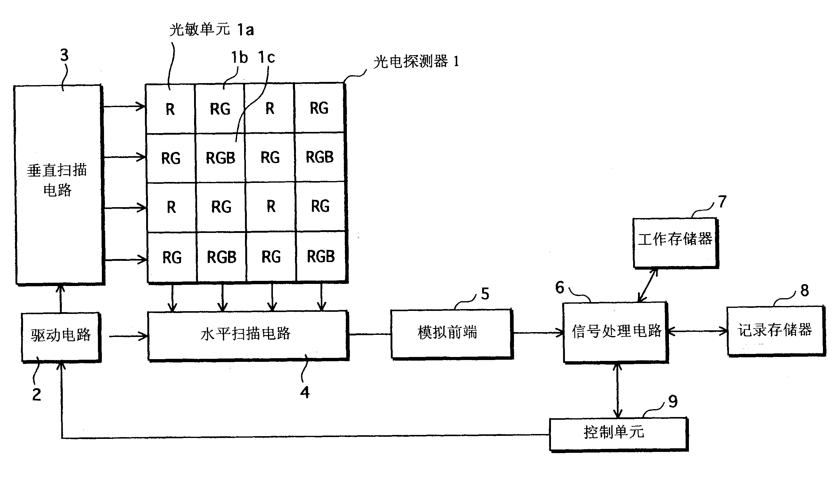
图1说明了根据本发明的成像系统的结构。Fig. 1 illustrates the structure of an imaging system according to the present invention.
该成像系统包括光电探测器1,驱动电路2,垂直扫描电路3,水平扫描电路4,模拟前端5,信号处理电路6,工作存储器7,记录存储器8,和控制单元9。The imaging system includes a
光电探测器1为所谓的MOS图像传感器,由形成在半导体衬底上的光敏单元(1a,1b,1c)构成。信号电荷根据相应的光敏单元预定波长范围内的光强产生在每个光敏单元中。图1的光敏单元分别标明R,RG,和RGB。“R”表示该单元设有透射红光波长范围内的光的滤色片,“RG”表示该单元设有透射红光波长范围和绿光波长范围内的光的滤色片,以及“RGB”表示该单元设有透射红光波长范围,绿光波长范围和蓝光波长范围内的光的滤色片。具体地,相应于红光波长范围内的光的信号电荷在光敏单元1a中产生。类似地,相应于红色和绿光波长范围内的光的信号电荷在光敏单元1b中产生,相应于红色,绿色和蓝光波长范围内的光的信号电荷在光敏单元1c中产生。同样,如图1所示,滤色片基本上基于Bayer模式图布置。在使用Bayer模式图的情况中,用于三种不同颜色的滤色片分配到四个像素单元。然而,滤色片的布置并不限于Bayer图案,也可以将用于四种不同颜色的滤色片分别分配到四个像素单元。The
在本说明书中,蓝光波长范围定义为小于490nm但不小于400nm,绿光波长范围定义为小于580nm但不小于490nm,红光波长范围定义为小于700nm但不小于580nm。进一步,小于400nm的波长范围定义为紫外波长范围,700nm以及更大的波长范围定义为红外波长范围。In this specification, the wavelength range of blue light is defined as less than 490nm but not less than 400nm, the wavelength range of green light is defined as less than 580nm but not less than 490nm, and the wavelength range of red light is defined as less than 700nm but not less than 580nm. Further, the wavelength range of less than 400nm is defined as the ultraviolet wavelength range, and the wavelength range of 700nm or greater is defined as the infrared wavelength range.
驱动电路2根据来自控制单元9的触发信号驱动垂直扫描电路3和水平扫描电路4。The driving
垂直扫描电路3基于来自驱动电路2的驱动信号循序逐行激活光敏单元。然后,垂直扫描电路3将一行已激活光敏单元中的信号电荷同时传输到水平扫描电路4。The
水平扫描电路4与垂直扫描电路3基于来自驱动电路2的驱动信号同时工作。对于每列,水平扫描电路4将一行传输来的信号电荷循序输出到模拟前端5。The
利用驱动电路2,垂直扫描电路3,和水平扫描电路4,将设置在矩阵中的光敏单元中的信号电荷转换为信号电压,然后将信号电压连续地输出到模拟前端5。Using the driving
模拟前端5取样并放大信号电压,通过进行A/D转换将模拟信号转换为数字信号,然后输出数字信号。The analog
信号处理电路6为数字信号处理器(DSP)。信号处理电路6将来自模拟前端5的数字信号转换为红色信号,绿色信号,和蓝色信号,并产生成像数据。The
当信号处理电路6将相应于光敏单元的数字信号转换为各自颜色的颜色信号时使用工作存储器7。工作存储器7的一个具体例子为SDRAM。The working
记录存储器8记录由信号处理电路6产生的成像数据。记录存储器8的一个具体例子为SDRAM。The
控制单元9控制驱动电路2和信号处理电路6。例如,控制单元9响应使用者按快门按钮的操作,输出触发信号到驱动电路2。The
下面详细地解释光电探测器1中光敏单元(1a,1b,1c)的结构。The structure of the photosensitive cells (1a, 1b, 1c) in the
图2为根据第一实施例的光敏单元(1a,1b,1c)的截面图。Fig. 2 is a cross-sectional view of a photosensitive unit (1a, 1b, 1c) according to a first embodiment.
每个光敏单元具有设置在掺杂了N型杂质的硅衬底11上的多个层结构。这些设置在硅衬底11上的层如下所述。Each photosensitive unit has a multi-layer structure disposed on a
光电二极管层12包括通过将P型杂质注入到衬底11中形成的P型阱16,和通过将N型杂质注入到P型阱16中形成的N型区光电转换单元17。The
绝缘层13为二氧化硅层,其设置的目的是为了将光电二极管层12和光屏蔽形成层14绝缘。The insulating layer 13 is a silicon dioxide layer, and its purpose is to insulate the
光屏蔽形成层14包括遮光层18,其由金属如铝和钨构成。用掩模掩盖相应于光屏蔽形成层14中小孔19的部分后,利用金属沉积或溅镀形成遮光层18。此外,除遮光层18外,光屏蔽形成层14还可以包括来自垂直扫描电路3和/或至水平扫描电路4的导线,信号电荷通过这些导线传输。The light-shielding forming
滤光形成层15包括由多晶硅构成的滤光层20。The
从光敏单元的上面部分进入的入射光22由微透镜21聚集,通过滤光层20和小孔19到达光电转换单元17。注意在说明中的入射光22已经通过光敏单元上方的红外截止滤光片(未在附图中示出),因此红外波长范围内的光已经被截止。The incident light 22 entering from the upper part of the photosensitive unit is collected by the microlens 21 , passes through the filter layer 20 and the small hole 19 and reaches the
滤光层20的厚度(ta,tb,tc)根据各自的光敏单元确定。The thickness (ta, tb, tc) of the filter layer 20 is determined according to each photosensitive unit.
通常,多晶硅具有这样的特性,即其截止波长根据其厚度确定,并且特定厚度的多晶硅层透射截止波长和更长波长的光,同时基本上截止波长小于截止波长的光。这里截止波长指光透射率开始低于一定比值的峰值透射率时的波长。严格地说,多晶硅也透射少量波长小于截止波长的光。然而,这样的光量小得趋于零,并且在形成信号电荷时没有太多贡献。因此,为了简化说明,波长小于截止波长的光在本说明书中描述为被截止。In general, polysilicon has a property that its cutoff wavelength is determined according to its thickness, and a polysilicon layer of a certain thickness transmits light of the cutoff wavelength and longer wavelengths while substantially cutting off light of a shorter wavelength than the cutoff wavelength. Here the cut-off wavelength refers to the wavelength at which the light transmittance begins to fall below a certain ratio of the peak transmittance. Strictly speaking, polysilicon also transmits a small amount of light with a wavelength smaller than the cutoff wavelength. However, such an amount of light is as small as zero and does not contribute much in forming signal charges. Therefore, for simplicity of description, light having a wavelength smaller than the cutoff wavelength is described as being cutoff in this specification.
在多晶硅的情况中,当厚度增大时,截止波长则变长。当多晶硅的厚度变薄时,截止波长则变短。In the case of polysilicon, as the thickness increases, the cutoff wavelength becomes longer. As the thickness of polysilicon becomes thinner, the cutoff wavelength becomes shorter.
具体地,通过调整每个光敏单元中滤光层20的厚度,可以在红光和绿光波长范围之间、绿色和蓝光波长范围之间、以及蓝色和紫外波长范围之间分别为光敏单元(1a,1b,1c)设定截止波长(λa,λb,λc)。Specifically, by adjusting the thickness of the filter layer 20 in each photosensitive unit, the photosensitive units can be divided between the wavelength range of red light and green light, between the wavelength range of green light and blue light, and between the wavelength range of blue light and ultraviolet light. (1a, 1b, 1c) Set cutoff wavelengths (λa, λb, λc).
当截止波长以该方式设定时,光敏单元1a中的信号电荷基于红光波长范围内的光产生,光敏单元1b中的信号电荷基于红光和绿光波长范围内的光产生,光敏单元1c中的信号电荷基于红光,绿光和蓝光波长范围内的光产生。When the cut-off wavelength is set in this way, the signal charges in the
具体地,光敏单元(1a,1b,1c)中滤光层20的截止波长(λa,λb,λc)如下设定:Specifically, the cut-off wavelengths (λa, λb, λc) of the filter layer 20 in the photosensitive unit (1a, 1b, 1c) are set as follows:
λa:580nmλa: 580nm
λb:490nmλb: 490nm
λc:400nmλc: 400nm
滤光层20相应于所列截止波长的厚度ta,tb和tc如下所示:The thicknesses ta, tb and tc of the filter layer 20 corresponding to the listed cutoff wavelengths are as follows:
ta:0.5μmta: 0.5 μm
tb:0.3μmtb: 0.3μm
tc:0.1μmtc: 0.1 μm
从而,可以通过光敏单元的滤光层20透射的光波长如下所示:Thus, the wavelengths of light that can be transmitted through the filter layer 20 of the photosensitive unit are as follows:
光敏单元1a:
580nm或更长(红光波长范围)580nm or longer (red wavelength range)
光敏单元1b:
490nm或更长(红光和绿光波长范围)490nm or longer (red and green wavelength range)
光敏单元1c:
400nm或更长(红光,绿光和蓝光波长范围)400nm or longer (red, green and blue wavelength range)
上述说明在图3中示出。The above description is shown in FIG. 3 .
图3为示出了多晶硅层和红外截止滤光片的光透射率的曲线图。FIG. 3 is a graph showing light transmittance of a polysilicon layer and an infrared cut filter.
曲线图中的曲线20a示出了厚度为0.5μm的多晶硅的透射特性,波长为580nm或更长的光透射通过该厚度。
曲线图中的曲线20b示出了厚度为0.3μm时多晶硅的透射特性,波长为490nm或更长的光透射通过该厚度。
曲线图中的曲线20c示出了厚度为0.1μm时多晶硅的透射特性,波长为400nm或更长的光透射通过该厚度。Curve 20c in the graph shows the transmission characteristics of polysilicon at a thickness of 0.1 μm through which light having a wavelength of 400 nm or longer is transmitted.
在第一实施例中,滤光层的厚度设定为ta=0.5μm,tb=0.3μm,以及tc=0.1μm。然而,ta,tb和tc的实际数值可以分别设定在0.01μm到2.0μm、0.01μm到1.5μm、以及0μm到1.0μm的范围内。In the first embodiment, the thickness of the filter layer is set to be ta=0.5 μm, tb=0.3 μm, and tc=0.1 μm. However, actual values of ta, tb, and tc may be set within the ranges of 0.01 μm to 2.0 μm, 0.01 μm to 1.5 μm, and 0 μm to 1.0 μm, respectively.
使这些厚度更薄的优点在于灵敏度提高,缺陷在于颜色分离变得困难,因为厚度ta,tb和tc之间的差值变得更小,从而透射光谱的差值也变得更小。另一方面,虽然光谱方面的差值更大使灵敏度降低,但优点在于颜色的分离更容易。The advantage of making these thicknesses thinner is that the sensitivity increases, the disadvantage is that the color separation becomes difficult because the difference between the thicknesses ta, tb and tc becomes smaller, and thus the difference in the transmission spectrum becomes smaller. On the other hand, although a greater difference in spectrum reduces sensitivity, the advantage is that the separation of colors is easier.
曲线图中的曲线20d示出了红外截止滤光片的透射特性,利用该滤光片波长等于或大于700nm的光被截止。
利用上述透射特性,在到光敏单元1a的入射光22中,仅在红光波长范围内的光通过滤光层20,到达光电转换单元17。类似地,在到光敏单元1b的入射光22中,仅在红光和绿光波长范围内的光到达光电转换单元17。同样,在到光敏单元1c的入射光22中,仅在红光,绿光和蓝光波长范围内的光到达光电转换单元17。Utilizing the above-mentioned transmission characteristics, among the incident light 22 to the
已经通过滤光层20透射的入射光22进一步通过小孔19。The incident light 22 that has been transmitted through the filter layer 20 further passes through the small hole 19 .
遮光层18设置在光电转换单元17的上方,以便防止相邻光敏单元中散射的光进入光电转换单元17。小孔19直接定位在光电转换单元17上。利用上述结构,基本垂直于衬底11的入射光到达光电转换单元17,与衬底成一定角度的光被阻挡。The light shielding layer 18 is disposed above the
光电转换单元17为通过具有p型阱16的pn结形成的光电二极管,并根据通过滤光层20和小孔19到达光电转换单元17的光强产生信号电荷。光电转换的机理如下所述。The
光电转换单元17具有耗尽区,其中载流子电子在结合了P型阱中载流子空穴后被耗尽。利用上述结构,光电转换单元17处的电势相对于P型阱16处的电势增加,因此,在耗尽区内产生内部电场。The
当上述情形中入射光22到达光电转换单元17时,电子空穴对通过光电转换产生,并且由于内部电场电子和空穴以相反的方向漂移。具体地,电子向光电转换单元17的中心漂移,空穴向P型阱漂移。结果,电子积聚在光电转换单元17中,在光敏单元中形成信号电荷。When the incident light 22 reaches the
因此,在光敏单元1a中,信号电荷根据入射光22中红光波长范围内的光强形成。类似地,在光敏单元1b中,信号电荷根据入射光22中红光和绿光波长范围内的光强形成。在光敏单元1c中,信号电荷根据入射光22中红光,绿光和蓝光波长范围内的光强形成。Therefore, in the
然而,根据上述结构,在光敏单元1b和1c中形成的信号电荷都包括多于一种颜色的信号。因此,为了根据光敏单元中的信号电荷产生成块的成像数据,必需通过处理基于光敏单元(1a,1b,1c)中信号电荷的数字信号(Sa,Sb,Sc)导出颜色信号(R,G,B)。下面解释信号处理的方法。However, according to the above structure, the signal charges formed in the
[信号处理][signal processing]
图4为说明了信号处理电路的内部结构的框图。FIG. 4 is a block diagram illustrating an internal structure of a signal processing circuit.
信号处理电路6包括矩阵保持单元61,计算单元62,和存储器控制单元63。The
矩阵保持单元61保持矩阵,该矩阵用于将模拟前端5中产生的数字信号(Sa,Sb,Sc)转换为颜色信号(R,G,B)。The
计算单元62通过将矩阵应用于数字信号(Sa,Sb,Sc)得到颜色信号(R,G,B)。
存储器控制单元63控制工作存储器7和记录存储器8的存取。The
图5A-5B示出了保持在矩阵保持单元61中的矩阵和逆矩阵。5A-5B show the matrix and the inverse matrix held in the
图5A示出了数字信号(Sa,Sb,Sc)和颜色信号(R,G,B)的关系。FIG. 5A shows the relationship between digital signals (Sa, Sb, Sc) and color signals (R, G, B).
在矩阵中,W11和其他系数表示基于滤光层20特性的加权因子。例如,当白光进入光敏单元1c时,在所有的红光,绿光和蓝光没有阻挡地通过的情况中,W11为0.333,W12为0.333,以及W13为0.333。在蓝光被稍微阻挡的情况中,可以做一些修正以便将W11设定得更小。进一步,在图5中,矩阵和逆矩阵的一些项的数字为0。然而,实际上每项通常为非0的数字。In the matrix, W11 and other coefficients represent weighting factors based on the characteristics of the filter layer 20 . For example, when white light enters the
图5B中示出的矩阵为保持在矩阵保持单元61中矩阵的逆矩阵。因此,通过对图5A中示出的矩阵进行逆变换得到该矩阵。图5B中示出的矩阵为图5A中示出的矩阵的逆矩阵,其为保持在矩阵保持单元61中的矩阵。The matrix shown in FIG. 5B is the inverse matrix of the matrix held in the
[存储器控制单元63的操作][Operation of Memory Control Unit 63 ]
存储器控制单元63将来自模拟前端5的数字信号暂时存储在工作存储器7中。当一幅图像的成像数据存储到工作存储器7时,存储器控制单元63从工作存储器7得到成像数据部分,并将这些数据输出到计算单元62。The
计算单元62将保持在矩阵保持单元61中的矩阵应用于输入的数据,得到颜色信号(R,G,B)。The
存储器控制单元63将计算单元62得到的颜色信号存储在记录存储器8中,并以颜色信号的形式构造一幅图像的成像数据。The
这样,一幅图像的成像数据记录在记录存储器8中。In this way, imaging data of one image is recorded in the
[制造方法][Manufacturing method]
接下来,解释制造滤光层20的方法。Next, a method of manufacturing the filter layer 20 is explained.
图6A-6H说明了制造滤光层20的方法的一个例子。An example of a method of manufacturing the filter layer 20 is illustrated in FIGS. 6A-6H.
图6A示出了化学汽相沉积(CVD)步骤后的光敏单元。在CVD步骤中,利用CVD将多晶硅层201形成在二氧化硅层的整个上表面上,该二氧化硅层已形成在光敏单元(1a,1b,1c)的光屏蔽形成层14中。多晶硅层201形成的厚度为0.5μm。Figure 6A shows the photosensitive cell after a chemical vapor deposition (CVD) step. In the CVD step, the
图6B示出了光致抗蚀剂涂覆步骤后的光敏单元。在光致抗蚀剂涂敷步骤中,光致抗蚀剂(PR)202施加到已经在CVD步骤中形成的多晶硅层201的整个上表面。Figure 6B shows the photosensitive cell after the photoresist coating step. In the photoresist coating step, a photoresist (PR) 202 is applied to the entire upper surface of the
图6C示出了曝光/显影步骤后的光敏单元。在曝光/显影步骤中,在以预定图案的掩模掩盖后,将在光致抗蚀剂涂覆步骤中形成的光致抗蚀剂202曝光,然后移除已曝光部分,将剩余部分硬化。通过该过程,光致抗蚀剂202只在相应于光敏单元1a的部分剩余,该部分在随后的干蚀刻步骤中不进行干蚀刻。Figure 6C shows the photosensitive cell after the exposure/development step. In the exposure/development step, after masking with a mask of a predetermined pattern, the
图6D示出了干蚀刻步骤后的光敏单元。在干蚀刻步骤中,对曝光/显影步骤后的多晶硅层201进行蚀刻。对多晶硅层201的光致抗蚀剂202没有保留的部分进行蚀刻,以便使多晶硅层201更薄。对多晶硅层201进行蚀刻使相应于光敏单元1b和1c的部分的厚度为0.3μm。Figure 6D shows the photosensitive cell after the dry etching step. In the dry etching step, the
当对多晶硅进行干蚀刻时,可以在干蚀刻中以±30nm的精确度控制薄膜厚度。When performing dry etching on polysilicon, the film thickness can be controlled with an accuracy of ±30 nm in dry etching.
图6E示出了光致抗蚀剂涂覆步骤后的光敏单元。在该步骤中,光致抗蚀剂(PR)203施加到多晶硅层201的整个上表面,与图6B所示的步骤类似。Figure 6E shows the photosensitive cell after the photoresist coating step. In this step, a photoresist (PR) 203 is applied to the entire upper surface of the
图6F示出了曝光/显影步骤后的光敏单元。在该步骤中,光致抗蚀剂203只在相应于光敏单元1a和1b的部分剩余,该部分在随后的干蚀刻步骤中不进行干蚀刻。Figure 6F shows the photosensitive cell after the exposure/development step. In this step, the
图6G示出了干蚀刻步骤后的光敏单元。在干蚀刻步骤中,对多晶硅层201的光致抗蚀剂203没有保留的部分进行蚀刻,以便使多晶硅层201更薄。对多晶硅层201进行蚀刻使相应于光敏单元1c的部分的厚度为0.1μm。Figure 6G shows the photosensitive cell after the dry etching step. In the dry etching step, the portion of the
图6H示出了光致抗蚀剂去除步骤后的光敏单元。在光致抗蚀剂去除步骤中,不需要的光致抗蚀剂203被去除。Figure 6H shows the photosensitive cell after the photoresist removal step. In the photoresist removal step,
通过上述步骤形成的多晶硅层201用作图2所示的滤光层20。The
如上所述,根据第一实施例的通过滤光层透射的光的波长范围由滤光层的厚度决定,而不是不同颜色的颜料或染料来确定。因此,在制造过程中控制不同颜色的颜料或染料的材料是不必要的,从而,可以减少生产成本。As described above, the wavelength range of light transmitted through the filter layer according to the first embodiment is determined by the thickness of the filter layer, not by different colors of pigments or dyes. Therefore, it is unnecessary to control the materials of different colors of pigments or dyes in the manufacturing process, and thus, the production cost can be reduced.
进一步,滤光层可以利用半导体制造技术来制造,并且管理丙烯酸树脂的滤色片制造过程不是必要的。结果,利用半导体制造的制造设备以及简化制造过程是可能的。Further, the filter layer can be manufactured using semiconductor manufacturing technology, and it is not necessary to manage the color filter manufacturing process of acrylic resin. As a result, it is possible to utilize manufacturing equipment for semiconductor manufacturing and to simplify the manufacturing process.
为了减少光透射,存在两种可能的方法。一种为使滤光层吸收光,另一种为使滤光层反射光。在本发明中,考虑到材料管理和眩光现象的发生,使用前面一种方法。眩光现象是正确的信号与来自于邻近光电转换单元的反射光的不正确信号重叠产生的现象。In order to reduce light transmission, there are two possible approaches. One is to make the filter layer absorb light, and the other is to make the filter layer reflect light. In the present invention, the former method is used in consideration of material management and occurrence of the glare phenomenon. The glare phenomenon is a phenomenon in which a correct signal overlaps an incorrect signal from reflected light from an adjacent photoelectric conversion unit.
后面一种方法通过例如具有交替设置的两种不同折射率的材料的多层结构来实现。在前面一种方法中,如上所解释,滤光层仅由一种材料(多晶硅,非晶硅,或硅)构成。因此,就材料管理来说,前面一种方法优于后面一种方法。The latter method is realized, for example, by a multilayer structure with two materials of different refractive index arranged alternately. In the former method, as explained above, the filter layer is composed of only one material (polysilicon, amorphous silicon, or silicon). Therefore, the former method is superior to the latter method in terms of material management.
此外,在后面一种方法中,没有透射过滤光层的光可以在被滤光层反射后通过在光电探测器中的散射到达邻近的光电转换单元。利用前面一种方法,没有透射过滤光层的光被滤光层吸收,因此眩光现象非常不容易出现。从而,就眩光现象的发生率来说,前面一种方法优于后面一种方法。In addition, in the latter method, the light not transmitted through the filter layer can reach the adjacent photoelectric conversion unit by scattering in the photodetector after being reflected by the filter layer. With the former method, the light not transmitted through the filter layer is absorbed by the filter layer, so the glare phenomenon is very unlikely to occur. Thus, the former method is superior to the latter method in terms of the occurrence rate of the glare phenomenon.
在第一实施例中,滤光层20的面向光源的主表面被折射率小于滤光层20的二氧化硅膜覆盖。这样的二氧化硅膜减小了入射光的折射率。通常,光电探测器位于气体如空气中,光在通过气体后到达滤光层。当气体和滤光层20具有直接接触时,它们的折射率之间的差值变大,从而在边界处的反射率变高。因此,在第一实施例中,通过在气体和滤光层20之间插入二氧化硅膜以减小反射率,从而灵敏度得到提高。In the first embodiment, the main surface of the filter layer 20 facing the light source is covered with a silicon dioxide film having a lower refractive index than the filter layer 20 . Such a silicon dioxide film reduces the refractive index of incident light. Usually, the photodetector is located in a gas such as air, and the light reaches the filter layer after passing through the gas. When the gas and the filter layer 20 have direct contact, the difference between their refractive indices becomes large, so that the reflectance at the boundary becomes high. Therefore, in the first embodiment, the sensitivity is improved by interposing a silicon dioxide film between the gas and the filter layer 20 to reduce the reflectance.
第二实施例second embodiment
[概要][summary]
在第二实施例中,滤光形成层15形成在光屏蔽形成层14下方,使滤光形成层15和光电二极管层12之间绝缘的绝缘层13形成以便具有1nm到150nm范围内的厚度。利用具有这种结构的光敏单元,入射光22在各层之间边界面的反射变得更小,因此,可以抑制灵敏度的降低。In the second embodiment, the
[结构][structure]
图7为根据第二实施例的光敏单元(1a,1b,1c)的截面图。Fig. 7 is a cross-sectional view of a photosensitive unit (1a, 1b, 1c) according to a second embodiment.
根据第二实施例的光敏单元每个都包括衬底11,光电二极管层12,绝缘层13,光屏蔽形成层14,和滤光形成层15。与第一实施例的光敏单元不同之处在于滤光形成层15形成在光屏蔽形成层14和绝缘层13之间。除该区别之外,第二实施例的光敏单元与第一实施例的光敏单元相同。因此,下面只对该区别进行解释。The photosensitive cells according to the second embodiment each include a
滤光形成层15包括由多晶硅构成的滤光层20,并且可以利用普通的半导体制造技术形成。因此,在光电二极管层12和光屏蔽形成层14之间形成滤光形成层15是可能的。The
由于滤光层20如上所述由多晶硅构成,因此如果滤光层20没有与光电二极管层12绝缘,则光电转换单元17中产生的信号电荷可能泄漏到滤光层20中。因此,厚度在1nm到150nm范围内的绝缘层13设置在滤光层20和光电二极管层12之间。Since the filter layer 20 is composed of polysilicon as described above, signal charges generated in the
厚度在1nm到150nm范围内的绝缘层13是第二实施例的光敏单元的特征部分。The insulating layer 13 having a thickness in the range of 1 nm to 150 nm is a characteristic part of the photosensitive unit of the second embodiment.
入射光22通过微透镜21聚集,经由小孔19和滤光层20到达光电转换单元17。一般而言,当光从具有较低折射率的另一介质进入具有较高折射率的介质时,光以一定比例在两个介质的边界面发生反射。The incident light 22 is collected by the microlens 21 and reaches the
入射光22通过的光敏单元中各层的材料和折射率如下:The material and refractive index of each layer in the photosensitive unit through which incident light 22 passes are as follows:
小孔19:由二氧化硅构成,折射率为1.45。Small hole 19: made of silicon dioxide, with a refractive index of 1.45.
滤光层20:由多晶硅构成,折射率为4。Filter layer 20 : made of polysilicon with a refractive index of 4.
绝缘层13:由二氧化硅构成,折射率为1.45。Insulating layer 13: made of silicon dioxide, with a refractive index of 1.45.
光电转换单元17:由N型硅构成,折射率为4。Photoelectric conversion unit 17 : made of N-type silicon with a refractive index of 4.
具体地,入射光22通过界面S1即滤光层20上表面,滤光层20和绝缘层13的界面S2,绝缘层13和光电转换单元17的界面S3,光在通过S1和S3时以一定比例反射。因此,到达光电转换单元17的光由于反射减少,结果,光敏单元的灵敏度降低。Specifically, the incident light 22 passes through the interface S1, that is, the upper surface of the filter layer 20, the interface S2 between the filter layer 20 and the insulating layer 13, and the interface S3 between the insulating layer 13 and the
已知通过将绝缘层13的厚度设定在1nm到150nm的范围内可以减小绝缘层13和光电转换单元17之间边界面的折射率。通过将绝缘层13的厚度设定在1nm到150nm的范围内,可以抑制光敏单元的灵敏度降低。It is known that the refractive index of the boundary surface between insulating layer 13 and
如上所解释,除第一实施例的光敏单元得到的效果之外,通过将绝缘层13的厚度设定在1nm到150nm的范围内从而减小入射光22的反射,第二实施例的光敏单元还具有抑制光敏单元灵敏度降低的效果。As explained above, in addition to the effect obtained by the photosensitive unit of the first embodiment, by setting the thickness of the insulating layer 13 in the range of 1 nm to 150 nm so as to reduce the reflection of the incident light 22, the photosensitive unit of the second embodiment It also has the effect of suppressing the reduction in sensitivity of the photosensitive unit.
第三实施例third embodiment
[概要][summary]
在第三实施例中,滤光层20与光电二极管层12之间的绝缘层13从光敏单元中去除以便提高光敏单元的灵敏度。然而,简单地移除绝缘层13会引起另一个问题,即光电转换单元17中产生的信号电荷泄漏到滤光层20中。因此,势垒23设置在光电转换单元17和滤光层20之间以便防止信号电荷泄漏。这样,可以完全地消除绝缘层13和光电二极管层12之间边界面的反射。In the third embodiment, the insulating layer 13 between the filter layer 20 and the
[结构][structure]
图8为根据第三实施例的光敏单元(1a,1b,1c)的截面图。Fig. 8 is a cross-sectional view of a photosensitive unit (1a, 1b, 1c) according to a third embodiment.
该光敏单元每个包括衬底11,光电二极管层12,光屏蔽形成层14,和滤光形成层15。与第二实施例的光敏单元不同之处在于没有包括绝缘层13。其他区别在于势垒23设置在光电转换单元17和滤光层20之间,以及迁移晶体管24设在每个光敏单元中,如附图中所示,用于光电转换单元17中产生的信号电荷的输送和非输送之间的切换。除这些区别之外,光敏单元与第二实施例的光敏单元相同。因此,下面只对区别进行解释。The photosensitive cells each include a
势垒23定位在光电转换单元17和滤光层20之间,在该势垒处产生势垒电势,同时该势垒通过在光电转换单元17中掺杂P型杂质形成。利用势垒23,防止了光电转换单元17中产生的信号电荷泄漏到滤光层20。进一步,如上所述,势垒23由硅构成,并且其折射率与滤光层20和光电转换单元17的折射率大致相同。因此,在这些层之间的界面(S4,S5)处入射光22几乎不发生反射。A potential barrier 23 is positioned between the
在迁移晶体管24中,漏极连接到光电转换单元17,源极24S连接到水平扫描电路4,栅极24G连接到垂直扫描电路3。因此,基于来自垂直扫描电路3的控制信号,可以转换光电转换单元17中产生的信号电荷的输送和非输送。In the
尽管没有在附图中示出,迁移晶体管24也设在每个光敏单元1b和1c中。而且,迁移晶体管24在其他实施例中也设在光敏单元中,但是没有详细描述,因为在其他实施例中迁移晶体管的具体描述不是必要的。Although not shown in the drawings, a
如上所述,在光敏单元中,势垒23的势垒电势防止光电转换单元17中的信号电荷泄漏到滤光层20。势垒23的细节将在下面描述。As described above, in the photosensitive cell, the barrier potential of the barrier 23 prevents signal charges in the
图9A和9B示出了光敏单元20的滤光层20、势垒23、光电转换单元17和迁移晶体管24的电势。9A and 9B show the potentials of the filter layer 20 , the potential barrier 23 , the
图9A示出了非输送时间内的电势。Fig. 9A shows the potential during the non-delivery time.
势垒23为P型半导体,其电势(势垒电势p2)由于与光电转换单元17形成的pn结而相对低于为N型半导体的光电转换单元17的电势(光电转换单元电势p3)。在非输送时间内,垂直扫描电路3控制使迁移晶体管24的栅极区的栅极电势p5变低。因此,势阱形成在光电转换单元17的位置处。Barrier 23 is a P-type semiconductor whose potential (barrier potential p2 ) is relatively lower than that of photoelectric conversion unit 17 (photoelectric conversion unit potential p3 ) which is an N-type semiconductor due to the pn junction formed with
通过光电转换在光电转换单元17中产生的电子在势阱中积聚成信号电荷Q1,随着信号电荷Q1积聚信号电势p4下降。Electrons generated in the
图9B示出了输送时间内的电势。Figure 9B shows the potential during delivery.
在输送时间内,垂直扫描电路3控制使得迁移晶体管24的栅极区的栅极电势p5升高,并与光电转换单元电势p3一样。通过这种方式控制,信号电荷Q1向源极24S迁移。During the transfer time, the
如上所述,势垒23通过形成势垒电势p2,防止信号电荷Q1泄漏到滤光层20。在势垒23没有设置的情况下,当信号电势p4下降到与滤光层电势p1相同时,信号电荷Q1可能泄漏到滤光层。As described above, the barrier 23 prevents the signal charge Q1 from leaking to the filter layer 20 by forming the barrier potential p2. In the case where the potential barrier 23 is not provided, when the signal potential p4 falls to be the same as the filter layer potential p1, the signal charge Q1 may leak to the filter layer.
势垒电势p2在输送时间内与栅极电势p5一起形成势阱,从而希望势垒电势p2设定为与栅极电势p5一样高,或者使得势垒高(电势小)于栅极电势p5。The barrier potential p2 forms a potential well together with the gate potential p5 during the transfer time, so it is desirable to set the barrier potential p2 as high as the gate potential p5 or to make the barrier higher (lower in potential) than the gate potential p5.
如上所述,除与第一实施例的光敏单元得到的效果相同之外,通过移除使滤光层20与光电二极管层12绝缘的绝缘层13,第三实施例的光敏单元还达到几乎完全消除在绝缘层13和光电二极管层12之间边界面的反射以及提高光敏单元灵敏度的效果。As described above, in addition to the same effect as the photosensitive unit of the first embodiment, by removing the insulating layer 13 that insulates the filter layer 20 from the
第四实施例Fourth embodiment
[概要][summary]
第四实施例的滤光层20通过在光电二极管层12的光电转换单元17的上部将P型杂质掺杂到光电转换单元17中形成。通过这种形成方法,与下述制造过程相比,可以缩短制造过程,该制造过程利用CVD形成具有预定厚度的多晶硅膜,然后进行蚀刻以便使每一薄膜具有相应于每个光敏单元的预定厚度。The filter layer 20 of the fourth embodiment is formed by doping P-type impurities into the
[结构][structure]
图10为根据第四实施例的光敏单元(1a,1b,1c)的截面图。Fig. 10 is a cross-sectional view of a photosensitive unit (1a, 1b, 1c) according to a fourth embodiment.
每个光敏单元包括衬底11,光电二极管层12,绝缘层13,和光屏蔽形成层14。与第一实施例的光敏单元的不同之处在于滤光层20形成在光电二极管层12的光电转换单元17上。除此之外,本实施例的光敏单元基本上与第一实施例的光敏单元相同。下面的描述仅涉及与第一实施例不同的部分。Each photosensitive cell includes a
滤光层20通过将P型杂质掺杂到光电转换单元17中形成。光敏单元的滤光层20的厚度(ta,tb,tc)如下设定,如第一实施例中一样:The filter layer 20 is formed by doping P-type impurities into the
ta:0.5μmta: 0.5 μm
tb:0.3μmtb: 0.3μm
tc:0.1μmtc: 0.1 μm
图11A-11C示出了电势和距离光敏单元中绝缘层13和光电二极管层12之间边界面S6的距离之间的联系。11A-11C show the relationship between the potential and the distance from the boundary surface S6 between the insulating layer 13 and the
图11A示出了光敏单元1a。FIG. 11A shows a
光敏单元1a的滤光层20厚度为0.5μm,入射光22中仅波长为580nm或更长的光(红光波长范围内的光)通过滤光层20,到达光电转换单元17。The thickness of the filter layer 20 of the
在光电转换单元17中,由于电势梯度(内部电场),通过光电转换产生的电子向光电转换单元17的中心漂移,空穴向滤光层20漂移。这样,将成为信号电荷的电子在光电转换单元17中积聚。In the
同时,由于滤光层20也由硅构成,因此由于入射光22中蓝光和绿光波长范围内的光产生电子空穴对。然而,电子空穴对不漂移,因为在滤光层20中没有形成电势梯度,如图11A所示。电子空穴对在一段时间后复合,然后消失。Meanwhile, since the filter layer 20 is also made of silicon, electron-hole pairs are generated due to light in the wavelength range of blue light and green light in the incident light 22 . However, the electron-hole pairs do not drift because no potential gradient is formed in the filter layer 20, as shown in FIG. 11A. The electron-hole pairs recombine after a while and then disappear.
因此,光敏单元1a的光电转换单元17中的信号电荷仅基于红光波长范围内的光产生。Therefore, signal charges in the
图11B示出了光敏单元1b。FIG. 11B shows the
光敏单元1b的滤光层20厚度为0.3μm,入射光22中仅波长为490nm或更长的光(红光和绿光波长范围内的光)通过滤光层20,到达光电转换单元17。The filter layer 20 of the
因此,光敏单元1b的光电转换单元17中的信号电荷基于红光和绿光波长范围内的光产生。Accordingly, signal charges in the
图11C示出了光敏单元1c。Figure 11C shows a
光敏单元1c的滤光层20厚度为0.1μm,入射光22中仅波长为400nm或更长的光(红光,绿光和蓝光波长范围内的光)通过滤光层20,到达光电转换单元17。The thickness of the filter layer 20 of the
因此,光敏单元1c的光电转换单元17中的信号电荷基于红光,绿光和蓝光波长范围内的光产生。Therefore, signal charges in the
[制造方法][Manufacturing method]
接下来,解释根据本实施例的一种制造滤光层20的方法。Next, a method of manufacturing the filter layer 20 according to the present embodiment is explained.
图12A-12G说明了制造滤光层20的方法的另一个例子。12A-12G illustrate another example of a method of manufacturing the filter layer 20. As shown in FIG.
滤光层20在形成光电转换单元17后通过P型杂质离子注入形成。The filter layer 20 is formed by implanting P-type impurity ions after the
图12A示出了离子注入步骤后的光敏单元。Figure 12A shows the photosensitive cell after the ion implantation step.
在离子注入步骤中,电离N型杂质(如磷和砷)或P型杂质(如硼),通过电场加速,然后注入到硅衬底等中。没有进行离子注入的区域通过光致抗蚀剂401覆盖保护。In the ion implantation step, N-type impurities such as phosphorus and arsenic or P-type impurities such as boron are ionized, accelerated by an electric field, and implanted into a silicon substrate or the like. Areas not subjected to ion implantation are covered and protected by
在附图所示的实施例中,光电转换单元17通过在P型阱16中掺杂N型杂质形成。In the embodiment shown in the drawings, the
图12B示出了离子注入步骤后的光敏单元。Figure 12B shows the photosensitive cell after the ion implantation step.
在离子注入步骤中,利用在形成光电转换单元17时使用的光致抗蚀剂401,通过P型杂质的离子注入到光电转换单元17中形成厚度为0.1μm的P型区域402。从而,形成光敏单元1c的滤光层。In the ion implantation step, a P-
在离子注入时根据注入离子的类型精确控制薄膜厚度的变化。例如当选择硼作为P型杂质时,可以控制在±3nm的精确度。During ion implantation, the variation of film thickness is precisely controlled according to the type of implanted ions. For example, when boron is selected as the P-type impurity, the accuracy of ±3nm can be controlled.
图12C示出了光致抗蚀剂涂覆步骤后的光敏单元。Figure 12C shows the photosensitive cell after the photoresist coating step.
在光致抗蚀剂涂覆步骤中,光致抗蚀剂403施加到衬底的整个上面部分。In the photoresist coating step,
然后,在曝光/显影步骤中,去除施加到将进行离子注入的部分的光致抗蚀剂403。Then, in the exposure/development step, the
图12D示出了离子注入步骤后的光敏单元。Figure 12D shows the photosensitive cell after the ion implantation step.
通过在光电转换单元1 7中掺杂P型杂质,形成厚度为0.3μm的P型区404。从而,形成光敏单元1b的滤光层。光敏单元1c通过光致抗蚀剂覆盖保护,因此对光敏单元1c没有进行离子注入。By doping P-type impurities in the
图12E示出了光致抗蚀剂涂覆步骤后的光敏单元。在光致抗蚀剂涂覆步骤中,光致抗蚀剂405施加到衬底的整个上面部分。Figure 12E shows the photosensitive cell after the photoresist coating step. In the photoresist coating step,
然后,在曝光/显影步骤中,施加到将进行离子注入部分的光致抗蚀剂405被去除。Then, in the exposure/development step, the
图12F示出了离子注入步骤后的光敏单元。Figure 12F shows the photosensitive cell after the ion implantation step.
通过在光电转换单元17中掺杂P型杂质,形成厚度为0.5μm的P型区域406。从而,形成光敏单元1a的滤光层。光敏单元1b和1c通过光致抗蚀剂覆盖和保护,因此对光敏单元1b和1c没有进行离子注入。By doping P-type impurities in the
图12G示出了光致抗蚀剂去除步骤后的光敏单元。在光致抗蚀剂去除步骤中,去除光致抗蚀剂405,因为它不再必要。因此,形成滤光层20。Figure 12G shows the photosensitive cell after the photoresist removal step. In the photoresist removal step, the
如上所解释,除实现第一实施例的光敏单元的效果之外,第三实施例的光敏单元还实现大程度的缩短制造过程的效果,因为滤光层20通过利用光电转换单元17形成时使用的相同光致抗蚀剂来形成。As explained above, in addition to realizing the effect of the photosensitive unit of the first embodiment, the photosensitive unit of the third embodiment also realizes the effect of shortening the manufacturing process to a large extent because the filter layer 20 is formed by using the
变形实施例Variations
尽管已经基于优选实施例解释了本发明的成像系统,但是本发明不限于上述实施例。本发明的其他可能形式包括如下所述的变形实施例。Although the imaging system of the present invention has been explained based on the preferred embodiments, the present invention is not limited to the above-described embodiments. Other possible forms of the invention include variant embodiments as described below.
(1)在优选实施例中,采用MOS图像传感器作为例子来进行说明。然而,本发明也可应用于CCD图像传感器。(1) In the preferred embodiment, a MOS image sensor is taken as an example for description. However, the present invention is also applicable to CCD image sensors.
(2)用于滤光层20的材料不限于多晶硅,可以是任意材料,只要不同波长范围内的光根据薄膜厚度透过该材料。例如,非晶硅可以用于滤光层20。(2) The material used for the filter layer 20 is not limited to polysilicon, and may be any material as long as light in different wavelength ranges passes through the material according to the film thickness. For example, amorphous silicon may be used for the filter layer 20 .
(3)滤光层20仅由多晶硅构成。然而,如果每一滤光层可以吸收波长大于预定波长的光多于波长小于所述波长的光,则本发明不限于该实施例。例如,滤光层可以为由不同材料构成的多层层状体的形式。(3) The filter layer 20 is made of polysilicon only. However, the present invention is not limited to the embodiment if each filter layer can absorb light having a wavelength greater than a predetermined wavelength more than light having a wavelength smaller than the wavelength. For example, the filter layer may be in the form of a multilayer laminate composed of different materials.
(4)相应于光敏单元1c的滤光层20还具有截止紫外区域中的光的功能。因此,在成像系统包括其他用于截止紫外光的装置的情况下,相应于光敏单元1c的滤光层20没有必要必须设置。普通成像系统中由透镜聚集的入射光在通过光学低通滤光片和红外截止滤光片后到达光电探测器1。在这种成像系统中,如果也设置了紫外截止滤光片,则在光电探测器1的光敏单元1c处没有必要截止紫外光。(4) The filter layer 20 corresponding to the
图13为成像系统设置了紫外截止滤光片的实施例的光敏单元(1a,1b,1c)的截面图。Fig. 13 is a cross-sectional view of the photosensitive unit (1a, 1b, 1c) of the embodiment in which the imaging system is provided with an ultraviolet cut filter.
如图13所示,相应于光敏单元1a的滤光层20的厚度为0.5μm,相应于光敏单元1b的滤光层20的厚度为0.3μm,相应于光敏单元1c的部分没有设置滤光层。As shown in Figure 13, the thickness of the filter layer 20 corresponding to the
(5)从第一到第三实施例,滤光层20都形成为光敏单元上的一体。因此,可以通过设定滤光层20的一个末端与接地电势(0V)连接为一体,另一末端与源电势(例如3V)连接为一体,从而在滤光层20内形成电势梯度,当入射光通过滤光层20时,滤光层20中产生的电子空穴对的电子被吸收到电源侧,空穴被吸收到接地侧。(5) In the first to third embodiments, the filter layer 20 is formed integrally on the photosensitive unit. Therefore, it is possible to form a potential gradient in the filter layer 20 by setting one end of the filter layer 20 to be connected to the ground potential (0V) as a whole, and the other end to be connected to the source potential (for example, 3V). When light passes through the filter layer 20, electrons of electron-hole pairs generated in the filter layer 20 are absorbed to the power supply side, and holes are absorbed to the ground side.
(6)为了将本发明应用于普通的数字静物相机或数字摄像机,光敏单元中滤光层20的厚度设定为ta=0.5μm,tb=0.3μm,以及tc=0.1μm。然而,在本发明用于其他目的的情况中,厚度不限于上述数值。(6) In order to apply the present invention to an ordinary digital still camera or digital video camera, the thickness of the filter layer 20 in the photosensitive unit is set to be ta=0.5 μm, tb=0.3 μm, and tc=0.1 μm. However, in the case where the present invention is used for other purposes, the thickness is not limited to the above-mentioned numerical value.
(7)严格地说,如图3所示,波长小于截止波长580nm的少量光通过了厚度为0.5μm的滤光层。具体地,除红光波长范围内的光以外,蓝光或绿光波长范围内的光某些程度上通过了光敏单元1a的滤光层。然而,基于波长小于截止波长的光的信号电荷小得趋于零,并且在形成信号电荷时没有太多贡献。因此,为了简化说明,本说明书中仅描述红光波长范围内的光通过了光敏单元1a的滤光层。类似地,波长小于截止波长的已经通过光敏单元1b和1c滤光层的少量光没有在说明书中考虑。(7) Strictly speaking, as shown in FIG. 3 , a small amount of light having a wavelength smaller than the cutoff wavelength of 580 nm passes through the filter layer having a thickness of 0.5 μm. Specifically, in addition to light in the red wavelength range, light in the blue or green wavelength range passes through the filter layer of the
由于上述原因,实施例中示出的矩阵和逆矩阵包括为0的项。然而,如果考虑波长小于截止波长的光的透射,则每项可以为非0的数值。The matrices and inverse matrices shown in the embodiment include entries of 0 for the reasons described above. However, if the transmission of light having a wavelength smaller than the cutoff wavelength is considered, each term may have a value other than 0.
(8)在实施例中,滤光层20形成为光敏单元1a,1b和1c上的一体。然而,滤光层20也可以独立形成。(8) In the embodiment, the filter layer 20 is formed integrally on the
(9)在实施例中,二氧化硅用作滤光层20面向光源的主表面上抗反射层的材料。然而,如果材料的折射率小于滤光层20的折射率,则抗反射层的材料不限于二氧化硅。例如,抗反射层可以由氮化硅或氮氧化硅(SiON)构成。(9) In the embodiment, silicon dioxide is used as a material for the antireflection layer on the main surface of the filter layer 20 facing the light source. However, the material of the anti-reflection layer is not limited to silicon dioxide if the refractive index of the material is smaller than that of the filter layer 20 . For example, the anti-reflection layer may be composed of silicon nitride or silicon oxynitride (SiON).
尽管本发明已经参照所附附图通过实施例进行了充分的描述,但是应当注意,多种改变和变形对于所属领域的技术人员是显而易见的。因此,除非这些改变和变形偏离了本发明的范围,否则它们应当认作包括在本发明的范围内。Although the present invention has been fully described through the embodiments with reference to the accompanying drawings, it is to be noted that various changes and modifications will be apparent to those skilled in the art. Therefore, unless otherwise these changes and modifications depart from the scope of the present invention, they should be construed as included therein.
Claims (21)
Applications Claiming Priority (2)
| Application Number | Priority Date | Filing Date | Title |
|---|---|---|---|
| JP2003388429 | 2003-11-18 | ||
| JP2003388429 | 2003-11-18 |
Publications (2)
| Publication Number | Publication Date |
|---|---|
| CN1638136A CN1638136A (en) | 2005-07-13 |
| CN100449764C true CN100449764C (en) | 2009-01-07 |
Family
ID=34567478
Family Applications (1)
| Application Number | Title | Priority Date | Filing Date |
|---|---|---|---|
| CNB2004100908893A Expired - Lifetime CN100449764C (en) | 2003-11-18 | 2004-11-16 | Photodetector |
Country Status (2)
| Country | Link |
|---|---|
| US (1) | US7262404B2 (en) |
| CN (1) | CN100449764C (en) |
Families Citing this family (68)
| Publication number | Priority date | Publication date | Assignee | Title |
|---|---|---|---|---|
| JP4806197B2 (en) * | 2005-01-17 | 2011-11-02 | パナソニック株式会社 | Solid-state imaging device |
| US7704782B2 (en) * | 2005-08-30 | 2010-04-27 | Aptina Imaging Corporation | Method of forming pixel cells with color specific characteristics |
| JP2007103401A (en) * | 2005-09-30 | 2007-04-19 | Matsushita Electric Ind Co Ltd | Imaging apparatus and image processing apparatus |
| US20070205354A1 (en) * | 2006-03-06 | 2007-09-06 | Micron Technology, Inc. | Image sensor light shield |
| JP4764243B2 (en) * | 2006-04-20 | 2011-08-31 | 株式会社東芝 | Solid-state imaging device |
| US7709872B2 (en) * | 2006-09-13 | 2010-05-04 | Taiwan Semiconductor Manufacturing Co., Ltd. | Methods for fabricating image sensor devices |
| KR20080058549A (en) * | 2006-12-22 | 2008-06-26 | 동부일렉트로닉스 주식회사 | Image sensor and manufacturing method of image sensor |
| KR100819706B1 (en) * | 2006-12-27 | 2008-04-04 | 동부일렉트로닉스 주식회사 | CMOS image sensor and manufacturing method |
| KR100829378B1 (en) * | 2006-12-27 | 2008-05-13 | 동부일렉트로닉스 주식회사 | Image sensor and its manufacturing method |
| US7935560B2 (en) * | 2007-09-06 | 2011-05-03 | International Business Machines Corporation | Imagers having electrically active optical elements |
| WO2009081971A1 (en) * | 2007-12-25 | 2009-07-02 | Seiko Instruments Inc. | Optical detection device, and image display device |
| JP2009158569A (en) * | 2007-12-25 | 2009-07-16 | Seiko Instruments Inc | Photodetection semiconductor device, photodetection device, and image display device |
| JP2009158570A (en) * | 2007-12-25 | 2009-07-16 | Seiko Instruments Inc | Photodetection semiconductor device, photodetection device, and image display device |
| DE102008016100A1 (en) * | 2008-03-28 | 2009-10-01 | Osram Opto Semiconductors Gmbh | Optoelectronic radiation detector and method for producing a plurality of detector elements |
| JP2009277798A (en) * | 2008-05-13 | 2009-11-26 | Sony Corp | Solid-state imaging device and electronic equipment |
| JP2010040805A (en) * | 2008-08-06 | 2010-02-18 | Oki Semiconductor Co Ltd | Illuminance sensor and method of manufacturing the same |
| JP2010103378A (en) * | 2008-10-24 | 2010-05-06 | Omron Corp | Photosensor |
| US8400537B2 (en) * | 2008-11-13 | 2013-03-19 | Omnivision Technologies, Inc. | Image sensors having gratings for color separation |
| US20100148291A1 (en) * | 2008-12-15 | 2010-06-17 | Tivarus Cristian A | Ultraviolet light filter layer in image sensors |
| JP5118661B2 (en) * | 2009-03-25 | 2013-01-16 | 浜松ホトニクス株式会社 | X-ray imaging device |
| US8330840B2 (en) * | 2009-08-06 | 2012-12-11 | Aptina Imaging Corporation | Image sensor with multilayer interference filters |
| JP5249994B2 (en) * | 2009-08-24 | 2013-07-31 | シャープ株式会社 | Semiconductor light detecting element and semiconductor device |
| WO2011053711A1 (en) | 2009-10-30 | 2011-05-05 | Invisage Technologies, Inc. | Systems and methods for color binning |
| JP2011100900A (en) | 2009-11-06 | 2011-05-19 | Sony Corp | Solid-state imaging apparatus and method of manufacturing and method of designing the same, and electronic apparatus |
| US8466000B2 (en) * | 2011-04-14 | 2013-06-18 | United Microelectronics Corp. | Backside-illuminated image sensor and fabricating method thereof |
| US20130010165A1 (en) | 2011-07-05 | 2013-01-10 | United Microelectronics Corp. | Optical micro structure, method for fabricating the same and applications thereof |
| US8866951B2 (en) | 2011-08-24 | 2014-10-21 | Aptina Imaging Corporation | Super-resolution imaging systems |
| US9312292B2 (en) | 2011-10-26 | 2016-04-12 | United Microelectronics Corp. | Back side illumination image sensor and manufacturing method thereof |
| US8318579B1 (en) | 2011-12-01 | 2012-11-27 | United Microelectronics Corp. | Method for fabricating semiconductor device |
| JPWO2013136820A1 (en) * | 2012-03-16 | 2015-08-03 | 株式会社ニコン | Imaging device and imaging apparatus |
| US8815102B2 (en) | 2012-03-23 | 2014-08-26 | United Microelectronics Corporation | Method for fabricating patterned dichroic film |
| US9401441B2 (en) | 2012-06-14 | 2016-07-26 | United Microelectronics Corporation | Back-illuminated image sensor with dishing depression surface |
| US8779344B2 (en) | 2012-07-11 | 2014-07-15 | United Microelectronics Corp. | Image sensor including a deep trench isolation (DTI)that does not contact a connecting element physically |
| US8828779B2 (en) | 2012-11-01 | 2014-09-09 | United Microelectronics Corp. | Backside illumination (BSI) CMOS image sensor process |
| US8779484B2 (en) | 2012-11-29 | 2014-07-15 | United Microelectronics Corp. | Image sensor and process thereof |
| US9279923B2 (en) | 2013-03-26 | 2016-03-08 | United Microelectronics Corporation | Color filter layer and method of fabricating the same |
| US9537040B2 (en) | 2013-05-09 | 2017-01-03 | United Microelectronics Corp. | Complementary metal-oxide-semiconductor image sensor and manufacturing method thereof |
| US9129876B2 (en) | 2013-05-28 | 2015-09-08 | United Microelectronics Corp. | Image sensor and process thereof |
| KR20150026223A (en) * | 2013-09-02 | 2015-03-11 | 에스케이하이닉스 주식회사 | Image sensor and method for fabricating the same |
| WO2015049981A1 (en) * | 2013-10-03 | 2015-04-09 | シャープ株式会社 | Photovoltaic conversion device |
| US9054106B2 (en) | 2013-11-13 | 2015-06-09 | United Microelectronics Corp. | Semiconductor structure and method for manufacturing the same |
| US9841319B2 (en) | 2013-11-19 | 2017-12-12 | United Microelectronics Corp. | Light detecting device |
| JP6115787B2 (en) * | 2013-12-18 | 2017-04-19 | ソニー株式会社 | Solid-state imaging device, manufacturing method thereof, and electronic apparatus |
| JP6416079B2 (en) * | 2014-03-31 | 2018-10-31 | 国立大学法人東北大学 | Solid-state light-receiving device for ultraviolet light |
| CN106104232B (en) * | 2014-04-04 | 2018-03-20 | 夏普株式会社 | Light-receiving device and portable electronic device |
| US9500787B2 (en) | 2014-04-23 | 2016-11-22 | Goodrich Corporation | Masked pixel arrays |
| US9978801B2 (en) * | 2014-07-25 | 2018-05-22 | Invisage Technologies, Inc. | Multi-spectral photodetector with light-sensing regions having different heights and no color filter layer |
| US9825078B2 (en) | 2014-11-13 | 2017-11-21 | Visera Technologies Company Limited | Camera device having an image sensor comprising a conductive layer and a reflection layer stacked together to form a light pipe structure accommodating a filter unit |
| US9911773B2 (en) | 2015-06-18 | 2018-03-06 | Omnivision Technologies, Inc. | Virtual high dynamic range large-small pixel image sensor |
| CN105115599A (en) * | 2015-08-17 | 2015-12-02 | 电子科技大学 | An Si-PIN four-quadrant photoelectric detector based on MEMS microstructure silicon and a manufacturing method thereof |
| US9955090B2 (en) * | 2016-07-20 | 2018-04-24 | Omnivision Technologies, Inc. | High dynamic range image sensor with virtual high-low sensitivity pixels |
| CN106328753A (en) * | 2016-08-26 | 2017-01-11 | 电子科技大学 | MEMS microstructure-based infrared-strengthened Si-PIN detector and preparation method thereof |
| CN106330313B (en) * | 2016-09-05 | 2017-11-10 | 京东方科技集团股份有限公司 | To box substrate, display panel and display device |
| JP6910704B2 (en) | 2016-12-13 | 2021-07-28 | ソニーセミコンダクタソリューションズ株式会社 | Image sensor, manufacturing method of image sensor, plasmon filter, and electronic equipment |
| JP7066316B2 (en) | 2016-12-13 | 2022-05-13 | ソニーセミコンダクタソリューションズ株式会社 | Image sensor and electronic equipment |
| WO2018123884A1 (en) * | 2016-12-27 | 2018-07-05 | 凸版印刷株式会社 | Solid-state imaging element and method for manufacturing same |
| JP6976067B2 (en) * | 2017-03-24 | 2021-12-01 | エイブリック株式会社 | Semiconductor device having an ultraviolet light receiving element and its manufacturing method |
| CN106886341B (en) * | 2017-03-28 | 2022-02-25 | 京东方科技集团股份有限公司 | Display substrate and display device |
| DE102019102176B4 (en) * | 2019-01-29 | 2022-11-24 | Senorics Gmbh | Hybrid multispectral component |
| CN109830495B (en) * | 2019-03-21 | 2021-10-08 | 京东方科技集团股份有限公司 | Array substrate and preparation method thereof, display device and imaging method thereof |
| US20210038080A1 (en) * | 2019-08-09 | 2021-02-11 | Maxim Integrated Products, Inc. | Optical diagnostic sensor systems and methods |
| US11536607B2 (en) | 2020-01-17 | 2022-12-27 | Samsung Electronics Co., Ltd. | Image sensor and method of operating |
| KR102825030B1 (en) * | 2020-07-20 | 2025-06-24 | 삼성전자주식회사 | Image sensor and electronic device |
| CN112490258B (en) * | 2020-12-25 | 2022-09-16 | 联合微电子中心有限责任公司 | Color CMOS image sensor pixel array, sensor and fabrication process |
| WO2022169501A1 (en) | 2021-02-03 | 2022-08-11 | Chowdhury Asif Jahangir | Silicon nitride waveguide coupled photodiode |
| US11810928B2 (en) * | 2021-05-17 | 2023-11-07 | Omnivision Technologies, Inc. | CMOS image sensor with LED flickering reduction and low color cross-talk |
| JP2024046470A (en) * | 2022-09-22 | 2024-04-03 | 株式会社東芝 | Solid-state imaging device |
| CN117238941B (en) * | 2023-11-15 | 2024-02-20 | 合肥晶合集成电路股份有限公司 | Backside illuminated image sensor and preparation method thereof |
Citations (6)
| Publication number | Priority date | Publication date | Assignee | Title |
|---|---|---|---|---|
| US5182624A (en) * | 1990-08-08 | 1993-01-26 | Minnesota Mining And Manufacturing Company | Solid state electromagnetic radiation detector fet array |
| JPH11289073A (en) * | 1998-04-06 | 1999-10-19 | Matsushita Electron Corp | Solid image pickup device and manufacture thereof |
| JP2000012814A (en) * | 1998-06-19 | 2000-01-14 | Sony Corp | Color solid-state imaging device with on-chip lens and method of manufacturing the same |
| JP2002094037A (en) * | 2000-09-18 | 2002-03-29 | Toppan Printing Co Ltd | Solid-state imaging device and method of manufacturing the same |
| US6482669B1 (en) * | 2001-05-30 | 2002-11-19 | Taiwan Semiconductor Manufacturing Company | Colors only process to reduce package yield loss |
| JP2003218336A (en) * | 2002-01-25 | 2003-07-31 | Toppan Printing Co Ltd | Method for manufacturing solid-state imaging device |
Family Cites Families (4)
| Publication number | Priority date | Publication date | Assignee | Title |
|---|---|---|---|---|
| JPH056986A (en) | 1991-06-27 | 1993-01-14 | Sharp Corp | Solid-state image sensing device |
| US5354989A (en) * | 1992-12-28 | 1994-10-11 | Advanced Fuel Research Inc. | Superconducting detector assembly and apparatus utilizing same |
| EP0678922A3 (en) | 1994-03-25 | 1997-04-09 | Matsushita Electronics Corp | Process for producing a solid-state image pickup device with colored layers. |
| US5766980A (en) | 1994-03-25 | 1998-06-16 | Matsushita Electronics Corporation | Method of manufacturing a solid state imaging device |
-
2004
- 2004-11-16 CN CNB2004100908893A patent/CN100449764C/en not_active Expired - Lifetime
- 2004-11-18 US US10/990,679 patent/US7262404B2/en not_active Expired - Lifetime
Patent Citations (6)
| Publication number | Priority date | Publication date | Assignee | Title |
|---|---|---|---|---|
| US5182624A (en) * | 1990-08-08 | 1993-01-26 | Minnesota Mining And Manufacturing Company | Solid state electromagnetic radiation detector fet array |
| JPH11289073A (en) * | 1998-04-06 | 1999-10-19 | Matsushita Electron Corp | Solid image pickup device and manufacture thereof |
| JP2000012814A (en) * | 1998-06-19 | 2000-01-14 | Sony Corp | Color solid-state imaging device with on-chip lens and method of manufacturing the same |
| JP2002094037A (en) * | 2000-09-18 | 2002-03-29 | Toppan Printing Co Ltd | Solid-state imaging device and method of manufacturing the same |
| US6482669B1 (en) * | 2001-05-30 | 2002-11-19 | Taiwan Semiconductor Manufacturing Company | Colors only process to reduce package yield loss |
| JP2003218336A (en) * | 2002-01-25 | 2003-07-31 | Toppan Printing Co Ltd | Method for manufacturing solid-state imaging device |
Also Published As
| Publication number | Publication date |
|---|---|
| CN1638136A (en) | 2005-07-13 |
| US20050103983A1 (en) | 2005-05-19 |
| US7262404B2 (en) | 2007-08-28 |
Similar Documents
| Publication | Publication Date | Title |
|---|---|---|
| CN100449764C (en) | Photodetector | |
| US7816169B2 (en) | Colors only process to reduce package yield loss | |
| US7955764B2 (en) | Methods to make sidewall light shields for color filter array | |
| JP4826111B2 (en) | Solid-state imaging device, manufacturing method of solid-state imaging device, and image photographing apparatus | |
| US9219090B2 (en) | Solid-state image capturing device and electronic device | |
| EP1570528B1 (en) | Cmos image sensor | |
| TW202139450A (en) | Method and structure to improve image sensor crosstalk | |
| JP2005175430A (en) | Light receiving element | |
| TWI569435B (en) | Image sensor with dielectric charge trapping device | |
| KR20070061530A (en) | Solid state imaging device | |
| US7208811B2 (en) | Photo-detecting device | |
| GB2382221A (en) | Image Sensor System | |
| US20150244958A1 (en) | Solid-state imaging device | |
| CN116636018A (en) | solid state imaging device | |
| JP5287923B2 (en) | Solid-state imaging device, manufacturing method of solid-state imaging device, and image photographing apparatus | |
| CN102169884B (en) | Solid-state imaging device, method of manufacturing thereof, and electronic apparatus | |
| CN108604590A (en) | solid state imaging device | |
| JP2006140413A (en) | Solid-state image sensor | |
| JP2014022649A (en) | Solid-state image sensor, imaging device, and electronic apparatus | |
| CN100470815C (en) | Solid State Image Sensor | |
| CN118866920B (en) | Imaging system, image sensor and preparation method thereof | |
| JPH04259256A (en) | Solid state image sensor | |
| TW202243300A (en) | Photodetector element | |
| JPH0590551A (en) | Solid-state imaging device | |
| KR20230033963A (en) | Image sensor and method for fabricating the same |
Legal Events
| Date | Code | Title | Description |
|---|---|---|---|
| C06 | Publication | ||
| PB01 | Publication | ||
| C10 | Entry into substantive examination | ||
| SE01 | Entry into force of request for substantive examination | ||
| C14 | Grant of patent or utility model | ||
| GR01 | Patent grant | ||
| CX01 | Expiry of patent term | ||
| CX01 | Expiry of patent term |
Granted publication date: 20090107 |