CN100421926C - Thermally stable polyethylene naphthalate films for flexible electronic and optoelectronic devices - Google Patents
Thermally stable polyethylene naphthalate films for flexible electronic and optoelectronic devices Download PDFInfo
- Publication number
- CN100421926C CN100421926C CNB02817576XA CN02817576A CN100421926C CN 100421926 C CN100421926 C CN 100421926C CN B02817576X A CNB02817576X A CN B02817576XA CN 02817576 A CN02817576 A CN 02817576A CN 100421926 C CN100421926 C CN 100421926C
- Authority
- CN
- China
- Prior art keywords
- film
- temperature
- layer
- thermally stable
- heat
- Prior art date
- Legal status (The legal status is an assumption and is not a legal conclusion. Google has not performed a legal analysis and makes no representation as to the accuracy of the status listed.)
- Expired - Fee Related
Links
Classifications
-
- B—PERFORMING OPERATIONS; TRANSPORTING
- B29—WORKING OF PLASTICS; WORKING OF SUBSTANCES IN A PLASTIC STATE IN GENERAL
- B29C—SHAPING OR JOINING OF PLASTICS; SHAPING OF MATERIAL IN A PLASTIC STATE, NOT OTHERWISE PROVIDED FOR; AFTER-TREATMENT OF THE SHAPED PRODUCTS, e.g. REPAIRING
- B29C55/00—Shaping by stretching, e.g. drawing through a die; Apparatus therefor
- B29C55/02—Shaping by stretching, e.g. drawing through a die; Apparatus therefor of plates or sheets
- B29C55/04—Shaping by stretching, e.g. drawing through a die; Apparatus therefor of plates or sheets uniaxial, e.g. oblique
- B29C55/06—Shaping by stretching, e.g. drawing through a die; Apparatus therefor of plates or sheets uniaxial, e.g. oblique parallel with the direction of feed
-
- B—PERFORMING OPERATIONS; TRANSPORTING
- B32—LAYERED PRODUCTS
- B32B—LAYERED PRODUCTS, i.e. PRODUCTS BUILT-UP OF STRATA OF FLAT OR NON-FLAT, e.g. CELLULAR OR HONEYCOMB, FORM
- B32B27/00—Layered products comprising a layer of synthetic resin
- B32B27/06—Layered products comprising a layer of synthetic resin as the main or only constituent of a layer, which is next to another layer of the same or of a different material
- B32B27/08—Layered products comprising a layer of synthetic resin as the main or only constituent of a layer, which is next to another layer of the same or of a different material of synthetic resin
-
- B—PERFORMING OPERATIONS; TRANSPORTING
- B32—LAYERED PRODUCTS
- B32B—LAYERED PRODUCTS, i.e. PRODUCTS BUILT-UP OF STRATA OF FLAT OR NON-FLAT, e.g. CELLULAR OR HONEYCOMB, FORM
- B32B27/00—Layered products comprising a layer of synthetic resin
- B32B27/36—Layered products comprising a layer of synthetic resin comprising polyesters
-
- C—CHEMISTRY; METALLURGY
- C08—ORGANIC MACROMOLECULAR COMPOUNDS; THEIR PREPARATION OR CHEMICAL WORKING-UP; COMPOSITIONS BASED THEREON
- C08J—WORKING-UP; GENERAL PROCESSES OF COMPOUNDING; AFTER-TREATMENT NOT COVERED BY SUBCLASSES C08B, C08C, C08F, C08G or C08H
- C08J5/00—Manufacture of articles or shaped materials containing macromolecular substances
- C08J5/18—Manufacture of films or sheets
-
- C—CHEMISTRY; METALLURGY
- C08—ORGANIC MACROMOLECULAR COMPOUNDS; THEIR PREPARATION OR CHEMICAL WORKING-UP; COMPOSITIONS BASED THEREON
- C08L—COMPOSITIONS OF MACROMOLECULAR COMPOUNDS
- C08L67/00—Compositions of polyesters obtained by reactions forming a carboxylic ester link in the main chain; Compositions of derivatives of such polymers
- C08L67/02—Polyesters derived from dicarboxylic acids and dihydroxy compounds
-
- H—ELECTRICITY
- H05—ELECTRIC TECHNIQUES NOT OTHERWISE PROVIDED FOR
- H05B—ELECTRIC HEATING; ELECTRIC LIGHT SOURCES NOT OTHERWISE PROVIDED FOR; CIRCUIT ARRANGEMENTS FOR ELECTRIC LIGHT SOURCES, IN GENERAL
- H05B33/00—Electroluminescent light sources
- H05B33/02—Details
-
- H—ELECTRICITY
- H10—SEMICONDUCTOR DEVICES; ELECTRIC SOLID-STATE DEVICES NOT OTHERWISE PROVIDED FOR
- H10K—ORGANIC ELECTRIC SOLID-STATE DEVICES
- H10K77/00—Constructional details of devices covered by this subclass and not covered by groups H10K10/80, H10K30/80, H10K50/80 or H10K59/80
- H10K77/10—Substrates, e.g. flexible substrates
- H10K77/111—Flexible substrates
-
- B—PERFORMING OPERATIONS; TRANSPORTING
- B29—WORKING OF PLASTICS; WORKING OF SUBSTANCES IN A PLASTIC STATE IN GENERAL
- B29K—INDEXING SCHEME ASSOCIATED WITH SUBCLASSES B29B, B29C OR B29D, RELATING TO MOULDING MATERIALS OR TO MATERIALS FOR MOULDS, REINFORCEMENTS, FILLERS OR PREFORMED PARTS, e.g. INSERTS
- B29K2067/00—Use of polyesters or derivatives thereof, as moulding material
-
- C—CHEMISTRY; METALLURGY
- C08—ORGANIC MACROMOLECULAR COMPOUNDS; THEIR PREPARATION OR CHEMICAL WORKING-UP; COMPOSITIONS BASED THEREON
- C08G—MACROMOLECULAR COMPOUNDS OBTAINED OTHERWISE THAN BY REACTIONS ONLY INVOLVING UNSATURATED CARBON-TO-CARBON BONDS
- C08G63/00—Macromolecular compounds obtained by reactions forming a carboxylic ester link in the main chain of the macromolecule
- C08G63/02—Polyesters derived from hydroxycarboxylic acids or from polycarboxylic acids and polyhydroxy compounds
- C08G63/12—Polyesters derived from hydroxycarboxylic acids or from polycarboxylic acids and polyhydroxy compounds derived from polycarboxylic acids and polyhydroxy compounds
- C08G63/16—Dicarboxylic acids and dihydroxy compounds
- C08G63/18—Dicarboxylic acids and dihydroxy compounds the acids or hydroxy compounds containing carbocyclic rings
- C08G63/181—Acids containing aromatic rings
- C08G63/185—Acids containing aromatic rings containing two or more aromatic rings
- C08G63/187—Acids containing aromatic rings containing two or more aromatic rings containing condensed aromatic rings
- C08G63/189—Acids containing aromatic rings containing two or more aromatic rings containing condensed aromatic rings containing a naphthalene ring
-
- C—CHEMISTRY; METALLURGY
- C08—ORGANIC MACROMOLECULAR COMPOUNDS; THEIR PREPARATION OR CHEMICAL WORKING-UP; COMPOSITIONS BASED THEREON
- C08J—WORKING-UP; GENERAL PROCESSES OF COMPOUNDING; AFTER-TREATMENT NOT COVERED BY SUBCLASSES C08B, C08C, C08F, C08G or C08H
- C08J2367/00—Characterised by the use of polyesters obtained by reactions forming a carboxylic ester link in the main chain; Derivatives of such polymers
- C08J2367/02—Polyesters derived from dicarboxylic acids and dihydroxy compounds
-
- H—ELECTRICITY
- H05—ELECTRIC TECHNIQUES NOT OTHERWISE PROVIDED FOR
- H05K—PRINTED CIRCUITS; CASINGS OR CONSTRUCTIONAL DETAILS OF ELECTRIC APPARATUS; MANUFACTURE OF ASSEMBLAGES OF ELECTRICAL COMPONENTS
- H05K1/00—Printed circuits
- H05K1/02—Details
- H05K1/03—Use of materials for the substrate
- H05K1/0313—Organic insulating material
- H05K1/032—Organic insulating material consisting of one material
- H05K1/0326—Organic insulating material consisting of one material containing O
-
- H—ELECTRICITY
- H10—SEMICONDUCTOR DEVICES; ELECTRIC SOLID-STATE DEVICES NOT OTHERWISE PROVIDED FOR
- H10K—ORGANIC ELECTRIC SOLID-STATE DEVICES
- H10K50/00—Organic light-emitting devices
- H10K50/80—Constructional details
- H10K50/84—Passivation; Containers; Encapsulations
- H10K50/844—Encapsulations
-
- H—ELECTRICITY
- H10—SEMICONDUCTOR DEVICES; ELECTRIC SOLID-STATE DEVICES NOT OTHERWISE PROVIDED FOR
- H10K—ORGANIC ELECTRIC SOLID-STATE DEVICES
- H10K59/00—Integrated devices, or assemblies of multiple devices, comprising at least one organic light-emitting element covered by group H10K50/00
- H10K59/80—Constructional details
- H10K59/87—Passivation; Containers; Encapsulations
- H10K59/873—Encapsulations
-
- Y—GENERAL TAGGING OF NEW TECHNOLOGICAL DEVELOPMENTS; GENERAL TAGGING OF CROSS-SECTIONAL TECHNOLOGIES SPANNING OVER SEVERAL SECTIONS OF THE IPC; TECHNICAL SUBJECTS COVERED BY FORMER USPC CROSS-REFERENCE ART COLLECTIONS [XRACs] AND DIGESTS
- Y02—TECHNOLOGIES OR APPLICATIONS FOR MITIGATION OR ADAPTATION AGAINST CLIMATE CHANGE
- Y02E—REDUCTION OF GREENHOUSE GAS [GHG] EMISSIONS, RELATED TO ENERGY GENERATION, TRANSMISSION OR DISTRIBUTION
- Y02E10/00—Energy generation through renewable energy sources
- Y02E10/50—Photovoltaic [PV] energy
- Y02E10/549—Organic PV cells
-
- Y—GENERAL TAGGING OF NEW TECHNOLOGICAL DEVELOPMENTS; GENERAL TAGGING OF CROSS-SECTIONAL TECHNOLOGIES SPANNING OVER SEVERAL SECTIONS OF THE IPC; TECHNICAL SUBJECTS COVERED BY FORMER USPC CROSS-REFERENCE ART COLLECTIONS [XRACs] AND DIGESTS
- Y02—TECHNOLOGIES OR APPLICATIONS FOR MITIGATION OR ADAPTATION AGAINST CLIMATE CHANGE
- Y02P—CLIMATE CHANGE MITIGATION TECHNOLOGIES IN THE PRODUCTION OR PROCESSING OF GOODS
- Y02P70/00—Climate change mitigation technologies in the production process for final industrial or consumer products
- Y02P70/50—Manufacturing or production processes characterised by the final manufactured product
-
- Y—GENERAL TAGGING OF NEW TECHNOLOGICAL DEVELOPMENTS; GENERAL TAGGING OF CROSS-SECTIONAL TECHNOLOGIES SPANNING OVER SEVERAL SECTIONS OF THE IPC; TECHNICAL SUBJECTS COVERED BY FORMER USPC CROSS-REFERENCE ART COLLECTIONS [XRACs] AND DIGESTS
- Y10—TECHNICAL SUBJECTS COVERED BY FORMER USPC
- Y10S—TECHNICAL SUBJECTS COVERED BY FORMER USPC CROSS-REFERENCE ART COLLECTIONS [XRACs] AND DIGESTS
- Y10S428/00—Stock material or miscellaneous articles
- Y10S428/91—Product with molecular orientation
-
- Y—GENERAL TAGGING OF NEW TECHNOLOGICAL DEVELOPMENTS; GENERAL TAGGING OF CROSS-SECTIONAL TECHNOLOGIES SPANNING OVER SEVERAL SECTIONS OF THE IPC; TECHNICAL SUBJECTS COVERED BY FORMER USPC CROSS-REFERENCE ART COLLECTIONS [XRACs] AND DIGESTS
- Y10—TECHNICAL SUBJECTS COVERED BY FORMER USPC
- Y10T—TECHNICAL SUBJECTS COVERED BY FORMER US CLASSIFICATION
- Y10T428/00—Stock material or miscellaneous articles
- Y10T428/24—Structurally defined web or sheet [e.g., overall dimension, etc.]
- Y10T428/24802—Discontinuous or differential coating, impregnation or bond [e.g., artwork, printing, retouched photograph, etc.]
-
- Y—GENERAL TAGGING OF NEW TECHNOLOGICAL DEVELOPMENTS; GENERAL TAGGING OF CROSS-SECTIONAL TECHNOLOGIES SPANNING OVER SEVERAL SECTIONS OF THE IPC; TECHNICAL SUBJECTS COVERED BY FORMER USPC CROSS-REFERENCE ART COLLECTIONS [XRACs] AND DIGESTS
- Y10—TECHNICAL SUBJECTS COVERED BY FORMER USPC
- Y10T—TECHNICAL SUBJECTS COVERED BY FORMER US CLASSIFICATION
- Y10T428/00—Stock material or miscellaneous articles
- Y10T428/31504—Composite [nonstructural laminate]
- Y10T428/31678—Of metal
- Y10T428/31681—Next to polyester, polyamide or polyimide [e.g., alkyd, glue, or nylon, etc.]
-
- Y—GENERAL TAGGING OF NEW TECHNOLOGICAL DEVELOPMENTS; GENERAL TAGGING OF CROSS-SECTIONAL TECHNOLOGIES SPANNING OVER SEVERAL SECTIONS OF THE IPC; TECHNICAL SUBJECTS COVERED BY FORMER USPC CROSS-REFERENCE ART COLLECTIONS [XRACs] AND DIGESTS
- Y10—TECHNICAL SUBJECTS COVERED BY FORMER USPC
- Y10T—TECHNICAL SUBJECTS COVERED BY FORMER US CLASSIFICATION
- Y10T428/00—Stock material or miscellaneous articles
- Y10T428/31504—Composite [nonstructural laminate]
- Y10T428/31786—Of polyester [e.g., alkyd, etc.]
-
- Y—GENERAL TAGGING OF NEW TECHNOLOGICAL DEVELOPMENTS; GENERAL TAGGING OF CROSS-SECTIONAL TECHNOLOGIES SPANNING OVER SEVERAL SECTIONS OF THE IPC; TECHNICAL SUBJECTS COVERED BY FORMER USPC CROSS-REFERENCE ART COLLECTIONS [XRACs] AND DIGESTS
- Y10—TECHNICAL SUBJECTS COVERED BY FORMER USPC
- Y10T—TECHNICAL SUBJECTS COVERED BY FORMER US CLASSIFICATION
- Y10T428/00—Stock material or miscellaneous articles
- Y10T428/31504—Composite [nonstructural laminate]
- Y10T428/31855—Of addition polymer from unsaturated monomers
- Y10T428/31938—Polymer of monoethylenically unsaturated hydrocarbon
Landscapes
- Chemical & Material Sciences (AREA)
- Engineering & Computer Science (AREA)
- Manufacturing & Machinery (AREA)
- Chemical Kinetics & Catalysis (AREA)
- Health & Medical Sciences (AREA)
- Medicinal Chemistry (AREA)
- Polymers & Plastics (AREA)
- Organic Chemistry (AREA)
- Materials Engineering (AREA)
- Mechanical Engineering (AREA)
- Laminated Bodies (AREA)
- Electroluminescent Light Sources (AREA)
- Manufacture Of Macromolecular Shaped Articles (AREA)
- Photovoltaic Devices (AREA)
Abstract
Use of a heat-stabilised, heat-set oriented film comprising polyethylene naphthalate as a substrate in or in the manufacture of an electronic or opto-electronic device comprising a conjugated conductive polymer, wherein the film has a shrinkage at 30 minutes at 230 ℃ of less than 1%; and a composite film comprising such a substrate layer and a barrier layer on the surface of the substrate layer.
Description
The present invention relates at flexible electronic device and opto-electronic device, particularly electroluminescent (EL) display device, and be suitable as PEN (PEN) film of base material in especially organic light emitting display (OLED) device.
Electroluminescent (EL) shows that be is the self-luminous display mode of feature with excellent legibility (comprising high brightness, high contrast, very fast response speed and wide visual angle), as thin as a wafer profile and extremely low energy consumption.The same self is luminous as cathode ray tube (CRT), fluorescence and plasma scope for the EL display device.They are different with LCD (LCD), need not back lighting.The response speed of EL can make this mode be particularly suitable for mobile image soon to 1000 times of LCD.The EL display can be used for numerous purposes, comprises aircraft and ships controller, automobile audiofrequency apparatus, calculator, mobile phone, laptop computer, instrument and meter, Plant supervisory device and electromedical equipment.Another main application of EL display is as light source, particularly as the back-lighting of little LCD dial plate so that they under low ambient lighting condition, be easy to read.
The EL display works by the film of phosphorus of double team in two boards or other electroluminescent material, and each plate comprises the conducting element of pre-setting sample, and promptly electrode forms addressable pixel thus on display.Described electrode is on the electroluminescent material or the coating that forms on independent carrier.When electrode energy printing opacity, when for example using the transparent conductive metal oxide, electrode is the form of translucent or clear coat.Equally, carrier can be translucent as required or transparent.In general, anode is transparent at least.Carrier plays electrode base board or usually as insulating barrier.Base material prevents chemistry and physically impaired effect when use, storage and transportation also are provided.Glass and polymer film etc. are arranged at present as insulating carrier.
The cathode material of EL display device use at present has many.Early stage researcher uses alkali metal.Other cathode material comprises metal composite, such as brass and conducting metal oxide (for example tin indium oxide).People also use various single metallic cathodes, such as indium, silver, tin, lead, magnesium, manganese and aluminium.
Nearest discovery comprises the device that various its organic light emitting mediums are made up of two thin layer that separate anode and negative electrode (gross thickness<1.0 μ m) in EL makes.The representative example of OLED device has the OLED that is disclosed among the US4720432 for example.
When electric current passed through conducting element, electroluminescent material was luminous.The EL display of switch light source all requires the application of high legibility particularly useful under all illumination conditions as luminous technics but not as LCD display.
The exploitation that can produce the trichromatic new organic electroluminescent material of extreme high purity makes and can prepare the even horizon light brightness of tool and the color monitor in life-span.Can be in solvent and by solution processing with polymer dissolution with this feature, make printable electronics.Conjugated conductive polymer is meaningful especially.Term " conductive conjugated polymer " used in this is meant the polymer that has π-electron delocalization effect along its main chain.Such polymer can be referring to W.J.Feast at Polymer, 37 volumes (22), 5017-5047, the summary in 1996.In an embodiment preferred, conductive conjugated polymer is selected from:
(i) hydrocarbon conjugated polymer, such as polyacetylene, polyphenylene and poly-(right-phenylenevinylene);
(ii) on main chain, has heteroatomic conjugation heterocycle polymer, such as polythiophene, polypyrrole and polyaniline; With
(iii) contain at least two, preferred at least three, preferred at least four, preferred at least five, the more preferably conjugated oligomer of six or more a plurality of repetition subunit, such as Oligopoly thiophene, low polypyrrole, Oligoaniline, low polyphenylene and oligomeric (phenylene vinylene).
Except being used for El element, there is the people that this conductive conjugated polymer is used for various other electronic devices and opto-electronic device, comprise photocell and semiconductor devices (such as organic field effect tube, thin film transistor (TFT) and universal integrated circuit).
The present invention relates to comprise the electronics of conductive conjugated polymer or the insulation and the carrier substrate of opto-electronic device, comprise the base material of El element (particularly OLED), photocell and semiconductor devices (such as organic field effect tube, thin film transistor (TFT) and universal integrated circuit).The present invention is specifically related to the base material of the base material of opto-electronic device, particularly El element (particularly OLED) or photronic base material, especially El element (particularly OLED).
Described base material can be transparent, translucent or opaque, but normally transparent.Described base material need satisfy the strict specification requirement of optical clarity, flatness and minimum two-fold rate usually.In general, for display applications, need all have 85% total light transmittance (TLT) in the interval of 400-800nm together with the mist degree that is lower than 0.7%.Require surface flatness and flatness can guarantee with the integrality of after-applied coating such as the electrodes conduct coating.Described base material also should have good barrier, promptly to the high patience of gas and solvent infiltration.The base material that is used for the electronic console purposes is fit to show and is lower than 10
-6G/m
2/ day moisture-vapor transmission and be lower than 10
-5/ mL/m
2The OTR oxygen transmission rate in/sky.Engineering properties such as flexibility, impact resistance, hardness and the trace of anti-picture property also are important consideration.
Previous optical quality glass or quartz are used as base material always in electronic display applications.These materials can satisfy the requirement of optics and planarization aspect and have good hear resistance and chemical resistance and barrier.Yet these materials do not have some required engineering properties, are apparent that low-density, flexibility and impact resistance most.
In order to improve mechanical performance, the someone proposes with plastic material instead of glass or quartz plate.Plastic basis material has the bigger flexibility and the impact resistance of improvement, and lighter than the glass or the quartz plate weight of same thickness.In addition, the flexiplast base material can allow for example to use above-mentioned conjugated polymer with the volume to volume method electronic device to be printed on the base material, but this can reduce the device of expense and production curvilinear surface.But the shortcoming of using polymeric material is the barrier of its lower chemical resistance and difference.But people have developed various barrier coats alleviates this problem.These coatings at high temperature apply with metallikon usually, thereby density and the morphosis that wherein can control coating obtain required barrier.Barrier layer can be organic barrier layer, also can be inorganic barrier layer, and it should show depositing the good compatibility of sedimentary deposit on it, and can form smooth surface.The material that is suitable for forming barrier layer is disclosed in for example US-6,198,217.In order to ensure the integrality and " acupuncture " that prevents wherein of barrier layer, surface of polymer substrates must show good slickness.
Yet, still have many restrictions with the plastic basis material of barrier layer coating.Specifically, the use of high-temperature technology such as spraying plating means that polymeric substrate must at high temperature keep size stability in the deposited barrier layers.Under the processing conditions of production display devices, particularly under the high temperature, the polymeric substrate of many types unacceptable size distortion can occur such as curling.These factors mean that the polymer film that has only some type is suitable as the base material of this device.In addition, in order to reduce the unstability of size, still need the temperature of the temperature of limit production process such as barrier layer deposition process.Because the quality of coating improves with the deposition process temperature usually, also need to provide the base material that under higher temperature, to process and keep dimensional stability simultaneously.In addition, because need other barrier layer usually for polymeric substrate, the expansion of proofreading and correct polymeric substrate thus with the expansion of barrier coat is avoided curling and keeping smooth thus.Because these reasons, the expansion characteristics of base material need less or measurable and preferably have both simultaneously.
The manufacturer of equipment, particularly handheld device such as the mobile phone of configuration electron display device uses the test that is called " thermal cycle " to estimate the performance of display device usually.This test comprises that the display circulation is exposed to pact arrives under about 80 ℃ temperature for-40 ℃, and each temperature has predetermined " retention time ", and arranged between temperature certain transit time, and can simulate the most extreme operating condition.
All be difficult to produce polymeric substrate with required size stability all the time.
So far, be applicable to the normally unbodied cast polymerization thing of the polymeric substrate film of electronic console purposes, comprise have higher glass transition temperature polymer such as the polyether sulfone and the polyimides of (Tg).Polymer with high Tg is welcome always, because the character of polymer can change more than Tg, particularly is difficult to prediction and control in the above dimensional stability of Tg.Except the problem of the film that is accompanied by production requirement dimensional stability and planarization, known film also can have the tendency that absorbs moisture, causes variable and uncertain expansion characteristics.In addition, the film that uses the solvent cast technology to produce may comprise residual solvent and need the degassing.
An object of the present invention is to provide a kind of film that overcomes at least a foregoing problems.Specifically, an object of the present invention is to provide and be suitable as base material a kind of comprising in the electronic device of conductive conjugated polymer or the opto-electronic device in production, the polymer film of the good high temperature dimensional stability of tool of flexible parent metal particularly, comprise and be used for El element (particularly OLED), the base material of photocell and semiconductor devices (such as organic field effect tube, thin film transistor (TFT) and universal integrated circuit).Another object of the present invention provides the polymer film of the good high temperature dimensional stability of tool, high optical transparency and excellent surface slickness/planarization.
According to the present invention, provide comprise PEN thermally-stabilised, heat setting alignment films in electronics that contains conductive conjugated polymer or opto-electronic device or in the manufacturing of these devices as the purposes of base material, wherein said film had at 230 ℃, 30 minutes and is lower than 1% shrinkage factor, and preferred wherein said film is being heated to 200 ℃ and be cooled to then before and after 8 ℃ of these processes at 25 ℃ of surplus size changes delta L that record from 8 ℃
rBe lower than full-sized 0.75%.
Used term " device that contains conductive conjugated polymer " preferably is meant El element (particularly OLED), photocell and semiconductor devices (such as organic field effect tube, thin film transistor (TFT) and universal integrated circuit) in this.Term " opto-electronic device that contains conductive conjugated polymer " used in this preferably is meant El element (particularly OLED) and photoelectric device, and especially preferably is meant El element (particularly OLED).The electronic device that used term contains conductive conjugated polymer in this does not comprise opto-electronic device, preferably is meant semiconductor devices such as organic field effect tube, thin film transistor (TFT) and universal integrated circuit, and organic field effect tube particularly.
Because temperature commonly used and with respect to the T of previous used polymer in this application in making with respect to described device
g, PENT
g(about 120 ℃) are lower, and the base material that PEN is suitable as this application is amazing.A particular advantage thermally-stabilised, the orientation pen film is that it allows to use higher temperature when barrier layer deposits.In addition, can obtain to have the pen film surface of high transparent and excellent surface slickness.With respect to polyethylene terephthalate (PET) film, another advantage of pen film for example is its lower moisture-vapor transmission and its lower OTR oxygen transmission rate.With regard to its much lower moisture absorption rate, have been found that pen film is better than amorphous high-tg polymer film discussed above.
After 230 ℃, 30 minutes described film preferably have be lower than 0.75%, more preferably less than 0.5%, again more preferably less than 0.25% shrinkage factor.In one embodiment, the shrinkage factor of described film after 230 ℃, 30 minutes is lower than 0.1%.Described film is being heated to 200 ℃ and be cooled to then before and after 8 ℃ of these processes in 25 ℃ of surplus size changes delta L that record from 8 ℃
rPreferably be lower than full-sized 0.5%, more preferably less than 0.25%, again more preferably less than 0.1%.Preferred described film has in-40 ℃ to+100 ℃ temperature range and is lower than 40 * 10
-6/ ℃, preferably be lower than 30 * 10
-6/ ℃, more preferably less than 25 * 10
-6/ ℃, again more preferably less than 20 * 10
-6/ ℃ thermal linear expansion coefficient (CLTE).
Described film is from film carrier, and it can independent existence under the situation of not carrying base in other words.
The thickness of described film is preferably about 12-300 μ m, 25-250 μ m more preferably from about, 50-250 μ m more preferably from about again.
The PEN polyester can be synthetic by conventional method.A kind of typical method relates to direct esterification or ester exchange reaction, and then carries out polycondensation.Therefore, the PEN polyester can be by with 2,5-, 2, and 6-or 2, the 7-naphthalenedicarboxylic acid (preferred 2,6-naphthalenedicarboxylic acid) or the condensation of its low alkyl group (6 carbon atoms at the most) diester and ethylene glycol obtain.In general, polycondensation reaction comprises solid state polymerization phase.Described solid phase can or carry out on the vacuum fluid bed of use rotary vacuum drier at the fluid bed of fluid bed such as nitrogen fluidisation.The solid phase technology that is fit to for example is disclosed among the EP-A-0419400, and this patent content is incorporated this paper by reference into.
In an embodiment preferred, described PEN uses the germanium catalyst preparation, and it provides the polymeric material of the level that has reduced pollutant such as catalyst residue, unwanted inorganic sediments and other polymeric by-products.As the result of " more cleaning " polymeric compositions, show improved optical transparence and surface smoothness by the film of its manufacturing.
The PEN that is used to prepare film of the present invention is fit to have 0.5-1.5, the PET-equivalent characteristic viscosity (IV of preferred 0.7-1.5, particularly 0.79-1.0; Mensuration as described herein).Be lower than 0.5 IV and cause polymer film to lack required character, and be difficult to obtain and may cause the difficulty of raw material processing greater than 1.5 IV such as engineering properties.
The formation of base material can be undertaken by the routine techniques that those skilled in the art are familiar with.The formation of base material is fit to be undertaken by extruding according to step described below.In general, described method comprises the step of extruding layer of molten polymer, quenching extrudate and at least one direction the extrudate of quenching being orientated.
Described base material can uniaxial orientation, but preferred biaxial orientation.Any method for preparing alignment films that orientation can be familiar with by those skilled in the art such as tubulose method (tubular process) or flat embrane method (flat film process) are carried out.Biaxial orientation is undertaken by stretching with two mutually perpendicular directions on the plane of film, to obtain the combination of gratifying engineering properties and physical property.
In the tubulose method, simultaneously biaxial orientation can be by by extruded thermoplastic polyester tube and quenching subsequently, reheating, expand by air pressure inside and cause horizontal orientation more then, and to cause machine-direction oriented speed to stretch.
In preferred flat embrane method, the polyester of formation base material is extruded by seam pattern head and is cooled off to guarantee that the polyester quenching becomes amorphous state fast on the casting drum of cooling.Then by under the temperature that is higher than described polyester glass transition temperature, be orientated at the stretch extrudate of this quenching of at least one direction.Orientation subsequently can be carried out at cross directional stretch then by the film stretching-machine at first at a direction (usually vertically, promptly directly to) the flat extrudate through quenching that stretches.Extrudate directly to stretch being fit to through one group of live-rollers or between two pairs of nip rolls, carrying out, cross directional stretch carries out on stenter then.Perhaps, orientation can be undertaken by stretching simultaneously in extruded film.Here, in the essentially identical stage of described processing, film stretches on vertical and horizontal in the stenter baking oven.For sequence stretching with the two kinds of approach that stretch simultaneously, the degree of stretching depends in part on the character of polyester.But described film is drawn into usually and is being of a size of full-sized 2 to 5 times, more preferably 2.5 to 4.5 times after its orientation on each draw direction.In general, be stretching in 70 ℃ to 150 ℃, carry out under common 70 ℃ to the 140 ℃ temperature.Can adopt bigger draw ratio (for example being up to about 8 times) if only need so a direction orientation.Need not stretch on an equal basis at vertical and horizontal, but then preferred equal stretching when needing the character of balance.
Stretched film is by at the glass transition temperature that is higher than described polyester but be lower than under the temperature of its melt temperature, and heat setting induces crystallizing polyester to carry out dimensionally stable under size limits, described in GB-A-838708.Usually in about 19-75kg/m film width, the preferred scope of about 45-50kg/m film width, for the wide film of about 2.6m, tension range is about 50-190kg to the tension force that size limits, preferably 120-130kg.The actual heat set temperature and time will be according to the composition of film and difference, thereby but should select can not reduce basically the tear resistance of film.In these restrictions, need about 135-250 ℃ heat-set temperature usually, more preferably 235-240 ℃ heat-set temperature.To depend on used temperature heat time heating time and be generally 5 to 40 seconds, preferred 8 to 30 seconds.
Then the film of finishing is passed through under low-tension (promptly minimum possible size restrictions), at the glass transition temperature that is higher than polyester but be lower than heating under the temperature of its fusing point and allow in film most of and (releases) to occur and come further thermally-stabilisedly shrinking, and very the low-residual shrinkage factor is also so have a film of high-dimensional stability to produce tool thus.The tension force that film stands in this thermally-stabilised step is usually less than 5kg/m film width, preferably is lower than 3.5kg/m, and more preferably the about 2.5kg/m of 1-is generally 1.5-2kg/m film width.The lateral dimension of film does not increase in thermally-stabilised step.The used temperature of thermally-stabilised step can be according to the required combination of telolemma character and difference, and temperature is high more, obtains good more promptly low more residual shrinkage.Usually need 135-250 ℃ temperature, preferred 190-250 ℃, more preferably 200-230 ℃, more preferably at least 215 ℃, general 215-230 ℃.Depend on used temperature heat time heating time, but be generally 10 to 40 seconds, the time in preferred 20 to 30 seconds.Thisly add thermally-stabilised processing and can be undertaken by the whole bag of tricks, comprise plane and vertical stratification also " off-line " as treatment step or " online " separately as the continuation of film production process.In one embodiment, thermally-stabilised " off-line " carries out.
Described base material can comprise one or more independent layers.The composition of each layer can be identical or different.For example, described base material can comprise that one deck, two-layer, three layers, four layers or five layers or more layer and typical sandwich construction can be AB, ABA, ABC, ABAB, ABABA or ABCBA type.Preferred described base material includes only one deck.When described base material comprises more than one deck, the preparation of base material can be undertaken by co-extrusion type easily, can be by independent nib while each film forming layer of co-extrusion of porous dies, then in conjunction with each still fusion the layer carry out, perhaps preferably undertaken by the single channel co-extrusion, wherein at first combination in the passage that leads to the die head aggregate pipe of the melt-flow of each polymer, extrude together and produce multi-layer polymer film from nib not having under the streamlined flow condition of mutually mixing then, it can be orientated and heat setting as mentioned above like that.The formation of multi-layer substrate also can be undertaken by the laminated technology of routine, for example by laminated together the carrying out of the second layer with the ground floor and the preformation of preformation, perhaps by carrying out on the second layer that ground floor is cast in preformation.
Described polymer film can suitably comprise the additive that is usually used in producing polymer film.Therefore, can sneak into reagent such as crosslinking agent, dyestuff, pigment, cavitation agent (voidingagent), lubricant, antioxidant, free radical scavenger, UV absorbent, heat stabilizer, fire retardant, anti-blocking agent, surfactant, slip agents, brightener, gloss modifying agent, prodegradant, viscosity modifier and dispersion stabilizer on demand.Specifically, one deck can comprise the processability that can improve when producing and the specific filler of crimpiness (windability).Described specific filler can for example be the mixture of particulate inorganic filler or inconsistent resin extender or two or more this fillers.
Here " inconsistent resin " be meant in the extruding of described film and under the maximum temperature in making not fusion or basically with the immiscible resin of polymer.The existence of incompatible resin causes void layer usually, this means that described layer comprises alveolate texture, comprises a certain proportion of at least independent blind bore crack.The incompatible resin that is fit to comprises and contains the homopolymers or the copolymer of the list-alpha-olefin of 6 carbon atoms at the most in polyamide and the olefin polymer, particularly molecule.Preferable material comprises low-density or high density olefins homopolymers (particularly polyethylene, polypropylene or poly 4-methylpene-1), olefin copolymer (particularly ethylene-propylene copolymer) or two or more these mixture of polymers.Can use random, block or graft copolymer.
Particulate inorganic filler comprises conventional inorganic filler, particularly metal or quasi-metal oxides, such as aluminium oxide, silica (particularly precipitated silica or diatomaceous silica and silica gel) and titanium dioxide, the carbonate of molochite and alkali metal salt such as calcium and barium and sulfate.Also can use glass particle.Described particulate inorganic filler can be space or non-lash types.The particulate inorganic filler that is fit to can be equal phase filling and be made up of such as independent titanium dioxide or barium sulfate single kind packing material or compound basically.Perhaps, at least a portion filler can be for heterogeneous, and basic filler combines with other modified component.For example, basic filler particles can use surface modifier such as pigment, soap, surfactant coupling agent or other modifier to handle to promote or to change the filler degree compatible with the substrate layer polyester.
Preferred particulate inorganic filler comprises titanium dioxide and silica.
Titanium dioxide granule can be anatase or rutile crystal type.Preferred major part of described titanium dioxide granule is rutile, more preferably at least 60% (weight), particularly at least 80%, also particularly about 100% (weight) is rutile.Described particle can be by standard method such as chloride process or sulfate process preparation.Described titanium dioxide granule can coating, preferably uses inorganic oxide such as aluminium, silicon, zinc, magnesium or its mixture coating.Preferred coatings includes organic compounds in addition, and such as aliphatic acid, the preference chain alkanol is fit to have 8 to 30 carbon atoms, preferred 12 to 24 carbon atoms.Polydiorganosiloxanepolyurea or poly-organohydrogensiloxanes such as dimethyl silicone polymer or polymethyl hydrogen siloxane all are suitable organic compounds.Described coating suitably is applied on the titanium dioxide granule with the form of water slurry.Inorganic oxide is deposited to the water slurry from water soluble compound such as sodium aluminate, aluminum sulfate, aluminium hydroxide, aluminum nitrate, silicic acid or sodium metasilicate.Based on the weight of titanium dioxide, the coating on titanium dioxide granule preferably has the inorganic oxide of 1-12% and preferably has the organic compound of 0.5-3%.
Described inorganic filler should be a filler in small, broken bits, and its volume distributed median median particle diameter (equivalent sphere diameter that is equivalent to all particle volumes 50%, on the integral distribution curve of volume %, read particle diameter, be commonly referred to " D (v; 0.5) " value) be preferably 0.01-7.0 μ m, more preferably 0.05-4.5 μ m, particularly 0.15-1.5 μ m.
The size distribution of inorganic filler particle also is an important parameter, and for example the existence of oversized particles may cause film to show ugly " fleck ", promptly can see with bore hole to have many filler particles in the film.Preferably do not exist actual particle size to surpass the inorganic filler particle of 30 μ m.The particle that surpasses this size can remove by the known method for sieving of this area people.But, removing all greater than aspect the particle of selected size, screening is success fully always.So in fact, the size of 99.9% inorganic filler particle should be no more than 30 μ m, preferably should be no more than 20 μ m, and more preferably should be no more than 10 μ m.The inorganic filler particle of preferred at least 90%, more preferably at least 95% volume is at average grain diameter ± 3.0 μ m, particularly ± 2.5 in the scope of μ m.
The particle diameter of filler particles can pass through electron microscope, the special counter of Cauer, analysis by sedimentation and static state or dynamic light scattering measurement.Be preferably based on the technology of laser light diffraction.Described median particle diameter can be by drawing a representative less than the integral distribution curve of selected size particles percent by volume and measure the 50th percentage and record.
The component of film can be mixed in a usual manner.For example, by mixing with the monomer reaction agent that forms described strata compound, or described component can change or do and mix or come and mixed with polymers by chemical combination in extruder by drum, and then cooling also is ground into particle or fragment usually.Also can use masterbatch preparation technology.
In an embodiment preferred, film of the present invention is optically transparent film, preferably according to standard A STM D1003 canonical measure, have<3.5%, preferred<2%, more preferably<1.5%, more more preferably≤1%, particularly less than 0.7% scatter visible light (mist degree).In one embodiment, mist degree is in the scope of 0.6-1%.According to standard A STM D 1003 standards, preferably the total light transmittance (TLT) in the 400-800nm scope is at least 75%, and preferably at least 80%, more preferably at least 85%.In this embodiment, the common just a small amount of existence of filler is no more than 0.5% of given layer weight usually and also preferably is lower than 0.2% (weight).
In one embodiment, described film is not only as defined above optical clear like that, and shows good processing properties and crimpiness.In this embodiment, the described film glass particle that to comprise about 50-1000ppm volume distributed median median particle diameter be 1.0-7.0 μ m and about 200-2000ppm on average substantially granularity (being exactly number average bead diameter) be the silica dioxide granule of 0.01-0.09 μ m.Described glass particle is preferably the solid glass pearl, no matter the viewpoint of selecting how, preferably has circular basically cross section.Require that each glass particle shows 1: 1 to 1: 0.5, preferred 1: 1 to 1: 0.8,1: 1 to 1: 0.9 length-width ratio d particularly
1: d
2(d here
1And d
2Be respectively the minimum and maximum size of particle).Described glass particle is not subjected to the restriction of its chemical composition, but preferably includes crown glass and/or Pyrex.No matter the viewpoint of selecting how, described silica granule preferably is essentially circular cross section.Typical basic silica granule need show 1: 1 to 1: 0.5 and preferred 1: 1 to 1: 0.8 length-width ratio d
1: d
2Contain glass and silica the layer other case description in US-5328755, this patent disclosure is incorporated this paper by reference into.
In another alternative embodiment, described film is opaque and highly-filled, preferably shows 0.1-2.0, more preferably 0.2-1.5, more preferably 0.25-1.25, more preferably 0.35-0.75 and printing opacity density (TOD) (the Sakura Densitometer of 0.45-0.65 particularly again; The PDA65 type; Transmission mode).Described film can be blended into by the opacifying agent with effective dose easily and make it opaque in the blend polymer.The opacifying agent that is fit to comprises the compound of aforesaid inconsistent resin extender, particulate inorganic filler or two or more this fillers.Based on the weight of described strata compound, the amount of the filler that exists in designated layer is preferably 1-30% weight, more preferably 3-20% weight, particularly 4-15% weight, especially 5-10% weight.
The surface of opaque coating preferably shows 60-120, the more preferably whitness index that records as described herein of 80-110, particularly 90-105, particularly 95-100 unit.
Described pen film also can comprise one or more other polymeric layers or dope layer.Any coating all preferred " online " carries out.
In one embodiment, in the one side of film, another coating can comprise " lubricious coating " processability and crimpiness to improve film.A kind of suitable lubricious coating can be for example optional also comprising such as at the acrylic acid of the crosslinking agent described in the EP-A-0408197 and/or the discontinuity layer of methacrylate polymer resin, and described patent disclosure is incorporated this paper by reference into.Another can be for comprising that with lubricant coating described patent disclosure is incorporated this paper by reference into as disclosed potassium silicate coating in No. 5925428, United States Patent (USP).
In one embodiment, described film is coated with the primer coating layer, and it has improved film to the cohesive of applied layer subsequently.The character of primer coating or adhesive phase and characteristic will depend on the character of applied layer subsequently, but generally can be selected from acrylate or methacrylate polymers resin.The material that is fit to comprises:
(i) (a) 35-40% (mole) alkyl acrylate, (b) 35-40% alkyl methacrylate, (c) 10-15% (mole) contain the comonomer of free carboxy such as itaconic acid and (d) copolymer of 15-20% (mole) aromatic sulfonic acid and/or its salt such as p styrene sulfonic acid, an one example is that described patent disclosure is incorporated this paper by reference into as the ethyl acrylate/methyl methacrylate/itaconic acid/p styrene sulfonic acid of the disclosed 37.5/37.5/10/15% of comprising (mole) ratio and/or the copolymer of its salt in EP-A-0429179; With
(ii) a kind of acrylic acid and/or methacrylate polymer resin, an one example is that described patent disclosure is incorporated this paper by reference into as the disclosed polymer that comprises about 35-60% (mole) ethyl acrylate, about 30-55% (mole) methyl methacrylate and about 2-20% (mole) Methacrylamide in EP-A-0408197.
Described primer coating layer or adhesive phase also can comprise crosslinking agent, and it plays crosslinked described composition and improves the cohesive of base material and crosslinked in also should be able to carrying out in composition.The crosslinking agent that is fit to comprises the optional oxyalkylated condensation product of melamine and formaldehyde.Primer coating layer or adhesive phase also can comprise crosslinking catalyst such as ammonium sulfate and promote the crosslinked of crosslinking agent.Other crosslinking agent and catalyst that is fit to is disclosed in EP-A-0429179, and this patent disclosure is incorporated this paper by reference into.
During use, described film also can be coated with barrier layer as mentioned above.This coating is familiar with by this area people and is at high temperature applied with metallikon usually.Be applicable to that the material that forms barrier layer for example is disclosed in the United States Patent (USP) 6,198,217.One organic barrier layer can be formed by for example photocurable monomer or oligomer or thermoplastic resin.Photocurable monomer or oligomer should have low volatility and high fusing point.The example of this monomer comprises acrylic acid three hydroxyl methyl esters classes, such as trimethylolpropane triacrylate, two (trimethylolpropane) tetraacrylate etc.; The long-chain acrylate is such as 1,6-hexanediyl ester, 1,6-hexanediol dimethacrylate etc.; With cyclohexyl esters of acrylic acid such as two cyclopentene oxygen ethyl propylene acid esters, two cyclopentene oxygen base acrylate, cyclohexyl methacrylate etc.The example of this oligomer comprises acrylate oligomer, epoxy acrylate oligomer, urethane acrylate oligomer, ether acrylate oligomer etc.Can use light trigger such as benzoin ether, benzophenone, acetophenone, ketal to wait cured resin.The example of the thermoplastic resin that is fit to comprises polyethylene, polymethyl methacrylate, PET etc.The routine techniques that these organic materials can be familiar with by any this area people is such as applying by vacuum moulding machine.
Inorganic barrier layer should be by showing low moisture permeability and the material of moisture stable being made.Example comprises that oxide is such as SiO
2, SiO, GeO, Al
2O
3Deng, nitride such as TiN, Si
3N
4Deng and metal such as Al, Ag, Au, Pt, Ni etc.Inorganic material can use vapor phase technology such as vacuum moulding machine, spraying plating to wait and apply under standard conditions.
Barrier layer can itself comprise one or more dispersion layers, and can comprise one or more organic layers and one or more inorganic layer.
In an embodiment preferred, barrier layer is that the moisture-vapor transmission with base material in the opto-electronic device is reduced to and is lower than 10
-6G/m
2/ day and OTR oxygen transmission rate be reduced to be lower than 10
- 5/ mL/m
2The layer in/sky.Can be for in the embodiment at another, barrier layer is that the moisture-vapor transmission with base material in the electronic device is reduced to and is lower than 10
-2G/m
2/ sky (preferably is lower than 10
-6G/m
2/ day) and OTR oxygen transmission rate is reduced to is lower than 10
-3/ mL/m
2/ sky (preferably is lower than 10
-5/ mL/m
2/ sky) film.
In case deposited barrier layer, layer subsequently (comprising electrode and conjugated conductive polymer) can apply according to the conventional production technology that this area people are familiar with.Described electrode can be the electrode that any this area people are familiar with, and for example is selected from those electrodes as herein described.In one embodiment, described electrode is a conducting metal oxide, preferred tin indium oxide.
The electronic device of the common indication of this paper and opto-electronic device comprise (or a plurality of) conjugated conductive polymer layer, two or more electrode and an one or more substrate layer.
In one embodiment of the invention, the term electroluminescence display device, particularly OLED (OLED) device is meant the display devices that comprises the luminous current-conducting conjugated polymer material layer between the layer that places two each self-contained electrodes, and the composite construction that wherein obtains places between two base materials (or carrier or nappe) layer.
In one embodiment of the invention, term photocell (photovoltaic cellphotocell) is meant the device that comprises the conjugated conductive polymer material layer between the layer that places two each self-contained electrodes, and the composite construction that wherein obtains places between two base materials (or carrier or nappe) layer.
In one embodiment of the invention, the term transistor is meant a kind of device that comprises at least one conjugated conductive polymer layer, gate electrode, source electrode and a drain electrode and one or more substrate layers.
According to another aspect of the present invention, a kind of composite membrane that comprises substrate layer and barrier layer in its surface is provided, wherein said base material is thermally-stabilised, heat setting, the alignment films that comprises PEN, it had at 230 ℃, 30 minutes and is lower than 1% shrinkage factor, and preferred wherein said film is being heated to 200 ℃ and be cooled to 8 ℃ of front and back then from 8 ℃, at 25 ℃ of surplus size changes delta L that record
rBe lower than full-sized 0.75%; And preferably in-40 ℃ to+100 ℃ temperature range, have and be lower than 40 * 10
-6/ ℃ thermal linear expansion coefficient (CLTE).In one embodiment, described base material obtains by the method that comprises following step:
(i) form the layer that comprises PEN;
(ii) stretch described layer at least one direction;
(iii) under size limits, be higher than the glass transition temperature of polyester but be lower than heat setting under the temperature of its melting temperature with the wide tension force of about 19-75kg/m film; With
(iv) at the tension force that is lower than 5kg/m film width be higher than the glass transition temperature of polyester but be lower than under the temperature of its melting temperature thermally-stabilised.
According to another aspect of the present invention, a kind of composite membrane is provided, it comprises substrate layer as described herein and barrier layer in its surface as described herein, and also is included in electrode layer and the optional conjugated conductive polymeric layer altogether that also comprises at least a portion on barrier layer surface.
According to another aspect of the present invention, the electronic device as described herein that a kind of preparation contains conductive conjugated polymer and base material or the method for opto-electronic device are provided, described method comprises following step:
(i) form the layer that comprises PEN;
(ii) stretch described layer at least one direction;
(iii) the wide tension force of wide and preferably about 45-50kg/m film is being higher than the glass transition temperature of polyester but is being lower than heat setting under the temperature of its melting temperature with about 19-75kg/m film under size limits; With
(iv) the 5kg/m film is wide, wide more preferably less than the 3.5kg/m film, more preferably the 1.0-2.5kg/m film is wide and be generally the wide tension force of 1.5-2.0kg/m film and be higher than the glass transition temperature of polyester but be lower than under the temperature of its melting temperature thermally-stabilised being lower than; With
(v) provide in the device thermally-stabilised, heat setting, alignment films as base material.
Step in the production of electronic device or opto-electronic device can comprise that also usefulness barrier layer coated heat is stable, the alignment films base material of heat setting; Provide electrode by at least a portion of barrier layer, applying conductive material; With the conjugated conductive polymer layer is provided.
Can use some character of following determination of test method polymer film:
(i) the film transparency can be estimated by using Gardner XL211 nephelometer to measure by the total light transmittance (TLT) and the mist degree (scattering sees through the percentage of visible light) of whole film thickness according to ASTM D-1003-61.
(ii) the transmitted light density (TOD) of film is used Macbeth Densitometer TR 927 (Dent ﹠amp; Woods Ltd, Basingstoke UK) measures under transmission mode.
(iii) dimensional stability can be just or (a) thermal linear expansion coefficient (CLTE) or (b) the temperature cycles method (film is heated to assigned temperature and subsequently the cooling back measure wherein along the length variations surplus of specifying axle) estimate.
Two kinds of measuring methods are all used according to known method calibration that is used for temperature, displacement, power, intrinsic distortion, baseline and furnace temperature location and the Thermomechanical AnalyserPE-TMA-7 (Perkin Elmer) that checks and are carried out.Described film uses elongation to analyze folder (extensionanalysis clamps) and measures.The required baseline of elongated clip uses very low-expansion sample (quartz) to obtain, and the CLTE precision and the degree of accuracy (depending on that scanning back baseline goes to subtract) use the standard substance of known CLTE value such as pure aluminium foil to estimate.The sample that is selected from known locations axle in original film sample uses the folder of about 12mm to space and is installed in the system, and is placed under the power that applies 75mN on the 5mm width.The power that applies is regulated according to film thickness, promptly guarantee consistent tension force, and film is not crooked along analysis axis.Sample length is standardized into the length of measuring under 23 ℃ of temperature.
In CLTE method of testing (a), sample is cooled to 8 ℃, stable back and is heated to 240 ℃ with 5 ℃/min from 8 ℃.CLTE value (α) obtains from following formula:
α=ΔL/(L×(T
2-T
1))
In the formula Δ L for measure at variations in temperature (T
2-T
1) variation of sample length in the scope, L is the raw sample length under 23 ℃.Up to Tg temperature (120 ℃), it is reliable that the CLTE value all is considered to.
Described data can be used as the function picture that the sample length that is normalized into 23 ℃ varies with temperature (%).
In temperature cycling test method (b), use the step be similar to method (a), wherein temperature circulates between the temperature of 8 ℃ and several risings.Like this, membrane sample is heated to 140 ℃, 160 ℃, 180 ℃ or 200 ℃ from 8 ℃, is cooled to 8 ℃ then.Before and after this processing, be determined at 25 ℃ along horizontal and vertical length, length variations Δ L
rBe calculated to be the percentage of raw footage.The result is as shown in table 2.
Step was measured by the measuring melt viscosity method below (iv) inherent viscosity (IV) was used.The converter measurement of flow rate by linking to each other of predrying extrudate by the calibration die head under known temperature and pressure with computer.The regression equation calculation melt viscosity value (log that computer program records from experiment
10Viscosity) and equivalent IV.By computer drawing IV to the time (minute) figure and calculate degradation rate.Figure was extrapolated to for 0 time obtains initial IV and equivalent melt viscosity.Die throat diameter is 0.020 inch, and the IV for the highest 0.80, melt temperature are 284 ℃, and the IV for>0.80, melt temperature are 295 ℃.
(v) measure by sample being placed one period scheduled time of heating furnace in the shrinkage factor of assigned temperature.Calculating is in the shrinkage factor % of heating front and back at the size changing rate % of assigned direction film.
(vi) surface roughness use the routine that this area people are familiar with noncontact, white light, change the interferometry analytical technology mutually and measure.Used instrument is a Wyko NT3300 surface profile analyzer.The useful feature data that can use this technology to obtain comprise:
Mean roughness (Ra): the mathematic(al) mean peak height that calculates by the meter area
R.m.s. roughness (Rq): the average peak height root mean square that calculates by the meter area
Maximum section peak height (Rp): the peak height at top in the meter area
Average maximum section peak height (Rpm): the mean value at ten tops in the meter area.
Roughness parameter and peak height are measured with respect to surface area of sample or " average line " of average level according to routine techniques.(polymer film surface may and not exclusively be put down, and often along its surface slight fluctuating is arranged.Described average line is the straight line that passes through from the middle part that rises and falls and apparent height departs from, and it is divided vertical section equally and makes the average line upper and lower have equal area.)
The surface profile analysis is undertaken by the zone of dispersion of scanning at " visual field " of surface profile analytical engine (it is the area that scans in the single measurement) intimal surface.Membrane sample can use discrete visual field or analyze by scanning continuous visual field formation display.The Wyko NT3300 surface profile analyzer of fine definition is used in the analysis of carrying out in this, and wherein each visual field comprises 736 * 480 pixels.
For the measurement of Ra and Rq, use object lens to improve resolution ratio with 50 x magnifications.The visual field that obtains has the size of 90 μ m * 120 μ m, and the Pixel Dimensions of tool 0.163 μ m.
For the measurement of Rp and Rpm, use to have 10 x magnifications and provide 5 times overall amplification together with " 0.5 times of visual field multiplier " and improve resolution ratio easily.The visual field that obtains has the size of 0.9mm * 1.2mm, is accompanied by the Pixel Dimensions of 1.63 μ m.
Concerning each was measured, five continuous sweep results obtained a mean value together.10% modulation theresholds (signal to noise ratio) is used in described measurement, and the data that promptly are lower than threshold value are discarded.
Preferred film of the present invention has and is lower than 0.8, preferably is lower than 0.7, preferably is lower than 0.65 and most preferably be lower than the Ra value of the measurement as described herein of 0.6nm.Preferred film of the present invention has 1.0nm or following, preferred 0.9nm or following, following 0.85nm or following, most preferably 0.75nm or the following Rq value of measuring as described herein.
(vii) OTR oxygen transmission rate can use ASTM D3985 to measure.
(vii) moisture-vapor transmission can use ASTM F1249 to measure.
(ix) whitness index of film outer surface uses Colorgard System 2000, and Model/45 (Pacific Scientific) measures according to ASTM D313.
The present invention will further specify by following embodiment.Should understand described embodiment just is used to illustrate and above-mentioned the present invention is not constituted qualification.Do not deviating from the modification that to make under the situation of the present invention on the details.
Embodiment
Embodiment 1
In the standard ester exchange reaction, make naphthalene diformic acid dimethyl ester in the presence of 400ppm manganese acetate tetrahydrate catalyst with glycol reaction, form naphthalenedicarboxylic acid two (2-ethoxy) ester and oligomer thereof.In ester exchange reaction latter stage, add 0.025% phosphoric acid stabilize agent, then add 0.04% antimony trioxide polycondensation catalyst.Carry out the reaction of standard discontinuous polycondensation and be about 0.50-0.675 (true PEN IV up to the inherent viscosity (IV) of PEN; PET equivalence IV0.75-1.00).
The polymer composition that comprises PEN is extruded and casts on the rotation polishing drum of heat.Then film is delivered to and moved ahead control unit and be stretched to its full-sized about 3.34 times through a series of temperature control rollers extruding direction there.Drawing temperature is about 133 ℃.Then with film by in the stenter baking oven under 138 ℃ and there film is stretched in the horizontal its full-sized about 4.0 times.Then this biaxially-stretched film is being reached as high as heat setting under about 238 ℃ temperature in cooling with before being rolled onto spool by conventional method.The film gross thickness is 125 μ m.
Biaxially-stretched film with heat setting launches also to relax by it by a series of four flotation stoves and by the minimum line tension force that the conveying that applies and control described film is complementary in proper order then.Then heat-staple film is rolled.Each of four stoves all laterally has three temperature control districts (left side, the neutralization right side):
The left, center, right
No. 1 stove 200 210 200
No. 2 stoves 200 210 200
No. 3 stoves 200 210 200
No. 4 stoves 195 205 195
The linear velocity of film is 15m/min in thermally-stabilised step.The tension force that is used for film (the former roller width of 1360mm) is 24-25N.
Embodiment 2
Surface temperature repeats the step of embodiment 1 under using in thermally-stabilised step:
The left, center, right
No. 1 stove 223 230 223
No. 2 stoves 223 230 223
No. 3 stoves 223 230 223
No. 4 stoves 218 225 218
Embodiment 3
In the standard ester exchange reaction, make naphthalene diformic acid dimethyl ester in the presence of 400ppm manganese acetate catalyst with glycol reaction (glycol: the ester molar ratio is 2.1: 1), form naphthalenedicarboxylic acid two (2-ethoxy) ester and oligomer thereof.In ester exchange reaction latter stage, add 0.025% phosphoric acid stabilize agent, then add 0.020% germanium dioxide polycondensation catalyst (133ppm Ge metal).Carry out the reaction of standard discontinuous polycondensation and be about 0.50-0.675 (true PEN IV up to the inherent viscosity (IV) of PEN; PET equivalence IV 0.75-1.00).According to the general step described in the embodiment 1 polyester that obtains is used to prepare film.
Embodiment 4
In the standard ester exchange reaction, make naphthalene diformic acid dimethyl ester in the presence of 210ppm manganese acetate tetrahydrate catalyst with glycol reaction, form naphthalenedicarboxylic acid two (2-ethoxy) ester and oligomer thereof.In ester exchange reaction latter stage, add the agent of 0.025wt% phosphoric acid stabilize, then add 0.036wt% antimony trioxide polycondensation catalyst.Carry out the reaction of standard discontinuous polycondensation and be about 0.50-0.675 (true PEN IV up to the inherent viscosity (IV) of PEN; PET equivalence IV 0.75-1.0).According to the step described in the embodiment 1 polyester is used to prepare film, difference is to move ahead and carries out under the temperature that is stretching in 3.1 draw ratio and 150-155 ℃; Cross directional stretch carries out under the temperature of 3.5 draw ratio and 145 ℃ and heat-set temperature is 234 ℃.Final film thickness is that 125 μ m and mist degree are 0.6%.
Use the shrinkage factor of the film of described analysis of experiments embodiment 1 and 2 herein, the results are shown in table 1.Will be at the pen film that does not have under the thermally-stabilised step to prepare with comparing (contrast 1) in the mode identical with embodiment 1.
Table 1: film shrinkage factor
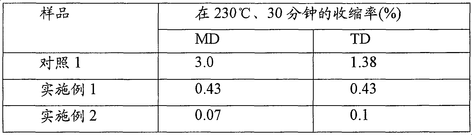
Even the result of table 1 shows that under higher temperature, the heat-set film of described heat stabilisation process also has good dimensional stability.The result also shows the improved shrinkage factor character of the heat stabilisation process of higher temperature (embodiment 2).
Use above-mentioned dimensional stability test method (iii) (b) analyze the film of embodiment 3 and 4.Will be by embodiment 4 preparation but do not have pen film that thermostabilization handles with comparing (contrasting 2).Horizontal (TD) and vertical (MD) at film measures.On behalf of film, negative value shrink.The results are shown in table 2.
The residue changes delta L of table 2. sample length
r

Data in the table 2 show and only show very little permanent change in size when heat-staple pen film is exposed to high temperature.Therefore just have favourable and predictable character as this film of the dimensional stability of temperature funtion and will be adapted in the electronic console as base material.On the contrary, do not have the pen film of heat stabilisation process to show the pucker ﹠ bloat effect, cause the bigger permanent deformation of film, after the particularly initial heating period.
The surface roughness of film also adopts method as herein described to measure, and it the results are shown in table 3.
Table 3. surface roughness
| Embodiment 1 | Embodiment 3 | |
| Mean roughness (Ra) | 0.64nm | 0.63nm |
| R.m.s. roughness (Rq) | 0.90nm | 0.82nm |
The result of table 3 shows that the polyester with Ge-catalysis has obtained excellent smoothness.
Claims (21)
Applications Claiming Priority (4)
| Application Number | Priority Date | Filing Date | Title |
|---|---|---|---|
| GBGB0122015.1A GB0122015D0 (en) | 2001-09-11 | 2001-09-11 | Polyester film |
| GB0122015.1 | 2001-09-11 | ||
| GB0208505.8 | 2002-04-12 | ||
| GB0208505A GB0208505D0 (en) | 2002-04-12 | 2002-04-12 | Polyester film II |
Related Child Applications (3)
| Application Number | Title | Priority Date | Filing Date |
|---|---|---|---|
| CN201210240432.0A Division CN102785419B (en) | 2001-09-11 | 2002-09-10 | Heat-stabilised poly(ethylene naphthalate) film for flexible electronic and opto-electronic devices |
| CN200810146087.8A Division CN101332694B (en) | 2001-09-11 | 2002-09-10 | Heat-stabilised poly(ethylene naphthalate) film for flexible electronic and opt-electronic devices |
| CN201210241091.9A Division CN102785420B (en) | 2001-09-11 | 2002-09-10 | Heat-stabilised poly(ethylene naphthalate) film for flexible electronic and opto-electronic devices |
Publications (2)
| Publication Number | Publication Date |
|---|---|
| CN1553856A CN1553856A (en) | 2004-12-08 |
| CN100421926C true CN100421926C (en) | 2008-10-01 |
Family
ID=26246534
Family Applications (3)
| Application Number | Title | Priority Date | Filing Date |
|---|---|---|---|
| CNB02817576XA Expired - Fee Related CN100421926C (en) | 2001-09-11 | 2002-09-10 | Thermally stable polyethylene naphthalate films for flexible electronic and optoelectronic devices |
| CN201210241091.9A Expired - Fee Related CN102785420B (en) | 2001-09-11 | 2002-09-10 | Heat-stabilised poly(ethylene naphthalate) film for flexible electronic and opto-electronic devices |
| CN201210240432.0A Expired - Fee Related CN102785419B (en) | 2001-09-11 | 2002-09-10 | Heat-stabilised poly(ethylene naphthalate) film for flexible electronic and opto-electronic devices |
Family Applications After (2)
| Application Number | Title | Priority Date | Filing Date |
|---|---|---|---|
| CN201210241091.9A Expired - Fee Related CN102785420B (en) | 2001-09-11 | 2002-09-10 | Heat-stabilised poly(ethylene naphthalate) film for flexible electronic and opto-electronic devices |
| CN201210240432.0A Expired - Fee Related CN102785419B (en) | 2001-09-11 | 2002-09-10 | Heat-stabilised poly(ethylene naphthalate) film for flexible electronic and opto-electronic devices |
Country Status (8)
| Country | Link |
|---|---|
| US (2) | US7101627B2 (en) |
| EP (2) | EP1425170B1 (en) |
| JP (2) | JP4623961B2 (en) |
| KR (2) | KR100857960B1 (en) |
| CN (3) | CN100421926C (en) |
| DE (2) | DE60223298T2 (en) |
| TW (1) | TW583233B (en) |
| WO (1) | WO2003022575A1 (en) |
Families Citing this family (53)
| Publication number | Priority date | Publication date | Assignee | Title |
|---|---|---|---|---|
| CN100421926C (en) * | 2001-09-11 | 2008-10-01 | 美国杜邦泰津胶片合伙人有限公司 | Thermally stable polyethylene naphthalate films for flexible electronic and optoelectronic devices |
| GB0208506D0 (en) | 2002-04-12 | 2002-05-22 | Dupont Teijin Films Us Ltd | Film coating |
| DE10314161A1 (en) * | 2003-03-28 | 2004-10-28 | Siemens Ag | Field effect electrodes for organic optoelectronic components |
| US7244893B2 (en) * | 2003-06-11 | 2007-07-17 | Belden Technologies, Inc. | Cable including non-flammable micro-particles |
| JP4820536B2 (en) * | 2003-06-25 | 2011-11-24 | 彬雄 谷口 | Method for manufacturing organic electroluminescence device |
| GB0405883D0 (en) * | 2004-03-16 | 2004-04-21 | Dupont Teijin Films Us Ltd | Polymeric film substrate |
| US7871691B2 (en) * | 2004-05-14 | 2011-01-18 | Teijin Dupont Films Japan Limited | Oriented polyester film |
| US7524920B2 (en) | 2004-12-16 | 2009-04-28 | Eastman Chemical Company | Biaxially oriented copolyester film and laminates thereof |
| GB0505517D0 (en) * | 2005-03-17 | 2005-04-27 | Dupont Teijin Films Us Ltd | Coated polymeric substrates |
| KR101287740B1 (en) * | 2005-04-08 | 2013-07-18 | 쓰리엠 이노베이티브 프로퍼티즈 컴파니 | Heat setting optical films |
| JP4683289B2 (en) * | 2006-01-13 | 2011-05-18 | 富士フイルム株式会社 | Method for producing thermoplastic resin film |
| WO2007092541A1 (en) * | 2006-02-08 | 2007-08-16 | 3M Innovative Properties Company | Method for manufacturing on a film substrate at a temperature above its glass transition |
| GB0602678D0 (en) * | 2006-02-09 | 2006-03-22 | Dupont Teijin Films Us Ltd | Polyester film and manufacturing process |
| DE102006016156A1 (en) * | 2006-04-06 | 2007-10-11 | Mitsubishi Polyester Film Gmbh | Hydrolysis resistant, multilayer polyester film with hydrolysis protection agent |
| EP2089458B1 (en) | 2006-09-28 | 2011-09-21 | 3M Innovative Properties Company | Method, system and its use for controlling curl in multi-layer webs |
| US8115326B2 (en) * | 2006-11-30 | 2012-02-14 | Corning Incorporated | Flexible substrates having a thin-film barrier |
| CA2680268C (en) * | 2007-03-09 | 2015-11-03 | 3M Innovative Properties Company | Multilayer film |
| WO2008144427A1 (en) * | 2007-05-18 | 2008-11-27 | Coopervision International Holding Company, Lp | Thermal curing methods and systems for forming contact lenses |
| EP2163572B1 (en) * | 2007-05-30 | 2014-08-13 | Teijin Dupont Films Japan Limited | Biaxially oriented polyester film for automobile driving motor and electrically insulating member composed of the same |
| KR20100089814A (en) * | 2007-08-02 | 2010-08-12 | 듀폰 테이진 필름즈 유.에스. 리미티드 파트너쉽 | Coated polyester film |
| US20090155958A1 (en) * | 2007-12-13 | 2009-06-18 | Boris Kolodin | Robust die bonding process for led dies |
| WO2009096390A1 (en) | 2008-01-31 | 2009-08-06 | Mitsubishi Plastics, Inc. | Gas barrier film having excellent weather resistance |
| US20090211622A1 (en) * | 2008-02-21 | 2009-08-27 | Sunlight Photonics Inc. | Multi-layered electro-optic devices |
| US20090215215A1 (en) * | 2008-02-21 | 2009-08-27 | Sunlight Photonics Inc. | Method and apparatus for manufacturing multi-layered electro-optic devices |
| US7842534B2 (en) | 2008-04-02 | 2010-11-30 | Sunlight Photonics Inc. | Method for forming a compound semi-conductor thin-film |
| KR101468937B1 (en) * | 2008-09-05 | 2014-12-11 | 코오롱인더스트리 주식회사 | Polyester film and manufacturing method thereof |
| US8110428B2 (en) * | 2008-11-25 | 2012-02-07 | Sunlight Photonics Inc. | Thin-film photovoltaic devices |
| JP5418505B2 (en) * | 2009-02-03 | 2014-02-19 | コニカミノルタ株式会社 | Organic electronic device and method for manufacturing the same |
| DE102009021712A1 (en) * | 2009-05-18 | 2010-11-25 | Mitsubishi Polyester Film Gmbh | Coextruded, biaxially oriented polyester films with improved adhesive properties, backside laminates for solar modules and solar modules |
| WO2011008459A2 (en) * | 2009-06-29 | 2011-01-20 | Infinite Corridor Technology, Llc | Structured material substrates for flexible, stretchable electronics |
| US8097297B2 (en) * | 2010-01-15 | 2012-01-17 | Korea Advanced Institute Of Science And Technology (Kaist) | Method of manufacturing flexible display substrate having reduced moisture and reduced oxygen permeability |
| GB201001947D0 (en) * | 2010-02-05 | 2010-03-24 | Dupont Teijin Films Us Ltd | Polyester films |
| KR101147988B1 (en) * | 2010-07-13 | 2012-05-24 | 포항공과대학교 산학협력단 | Method of manufacturing flexible electronic device using physical peel-off method, flexible electronic device and flexible substrate |
| KR101801096B1 (en) * | 2010-12-17 | 2017-11-24 | 삼성전자주식회사 | Transparent and flame retarding polyester resin composition and preparation method thereof |
| EP2487218A1 (en) * | 2011-02-09 | 2012-08-15 | Koninklijke Philips Electronics N.V. | Polymeric matrix with organic phosphor and manufactory thereof |
| TWI469872B (en) | 2011-12-13 | 2015-01-21 | Ind Tech Res Inst | Polyester films with low thermal expansion and methods for manufacturing the same |
| EP2794716B1 (en) * | 2011-12-19 | 2017-02-08 | DuPont Teijin Films U.S. Limited Partnership | Copolyesterimides of poly(alkylene naphthalate)s having high glass transition temperature and film made therefrom |
| CN104024224B (en) | 2011-12-21 | 2016-01-20 | 杜邦帝人薄膜美国有限公司 | There is the copolyester imide of poly-(the terephthalic acid alkylene ester) of high glass-transition temperature and film prepared therefrom |
| DE102012002448A1 (en) | 2012-02-08 | 2013-08-08 | Mitsubishi Polyester Film Gmbh | Coextruded, biaxially oriented polyester film with oligomer barrier |
| JP2013249329A (en) * | 2012-05-30 | 2013-12-12 | Canon Inc | Resin composition, formed article, and mirror |
| GB201310837D0 (en) | 2013-06-18 | 2013-07-31 | Dupont Teijin Films Us Ltd | Polyester film -IV |
| US20150029681A1 (en) * | 2013-07-29 | 2015-01-29 | Evonik Industries Ag | Flexible composite, production thereof and use thereof |
| GB201317705D0 (en) | 2013-10-07 | 2013-11-20 | Dupont Teijin Films Us Ltd | Copolyesters |
| TWI495680B (en) | 2013-11-07 | 2015-08-11 | Ind Tech Res Inst | Polyester composition, electronic device, and method of forming film |
| GB201411044D0 (en) | 2014-06-20 | 2014-08-06 | Dupont Teijin Films Us Ltd | Copolyestermides and films made therefrom |
| US10054727B2 (en) * | 2014-07-18 | 2018-08-21 | Teijin Limited | Uniaxially stretched multi-layer laminate film, and optical member comprising same |
| GB2523859B (en) | 2014-08-01 | 2016-10-19 | Dupont Teijin Films U S Ltd Partnership | Polyester film assembly |
| WO2016126866A1 (en) * | 2015-02-04 | 2016-08-11 | Conde Systems, Inc. | Curved acrylic decorated article |
| KR102421570B1 (en) * | 2015-10-02 | 2022-07-15 | 에스케이이노베이션 주식회사 | Manufacturing method for polymer film |
| JP2017105013A (en) * | 2015-12-08 | 2017-06-15 | 株式会社リコー | Gas barrier laminate, semiconductor device, display element, display device and system |
| CN107791606B (en) * | 2016-08-29 | 2021-07-23 | 东丽先端材料研究开发(中国)有限公司 | Films for organic EL applications, as well as organic EL displays and organic EL lighting |
| KR102054190B1 (en) * | 2017-01-23 | 2019-12-10 | 동우 화인켐 주식회사 | High performance film type touch sensor and manufacturing method thereof |
| TW202432360A (en) | 2022-12-14 | 2024-08-16 | 德商巴斯夫塗料有限責任公司 | Multilayer barrier film coated polymeric substrate, its manufacture and use in electronic devices |
Citations (1)
| Publication number | Priority date | Publication date | Assignee | Title |
|---|---|---|---|---|
| US5858490A (en) * | 1993-06-10 | 1999-01-12 | Nkk Corporation | Film formed from polyethylene-2,6-naphthalate resin, process for producing said film and package using said film |
Family Cites Families (55)
| Publication number | Priority date | Publication date | Assignee | Title |
|---|---|---|---|---|
| JPS4829541B1 (en) * | 1969-06-13 | 1973-09-11 | ||
| US3875119A (en) * | 1970-12-22 | 1975-04-01 | Hiroshi Aoki | Product and process of producing biaxially oriented insulating film of polyethylene-2,6-naphthalate |
| JPS5988719A (en) | 1982-11-15 | 1984-05-22 | Diafoil Co Ltd | Polyester film for base material of liquid crystal panel |
| JPS6151323A (en) | 1984-08-22 | 1986-03-13 | Toray Ind Inc | Preparation of uniaxially stretched polyester film for liquid crystal display |
| JPS62135338A (en) | 1985-12-09 | 1987-06-18 | Diafoil Co Ltd | Monoaxially high-orientated film of polyethylene-naphthalate for liquid crystal panel substrate |
| JPS62136013A (en) | 1985-12-09 | 1987-06-19 | ダイアホイルヘキスト株式会社 | Polyethylene-2,6-naphthalate film for capacitor |
| JPS62135339A (en) | 1985-12-09 | 1987-06-18 | Diafoil Co Ltd | Polyethylene-2,6-naphthalate film for magnetic recording medium |
| JPH0625267B2 (en) | 1985-12-17 | 1994-04-06 | ダイアホイルヘキスト株式会社 | Polyethylene-2,6-naphthalate film for high density magnetic recording media |
| JPS6342845A (en) | 1986-08-11 | 1988-02-24 | Diafoil Co Ltd | Polyester film for liquid crystal indication |
| US4734174A (en) * | 1986-12-17 | 1988-03-29 | Polaroid Corporation | Electrochemical formation of thin-film electrodes |
| JP2526642B2 (en) * | 1988-08-30 | 1996-08-21 | 東洋紡績株式会社 | Transparent conductive film |
| JPH02251428A (en) * | 1989-03-27 | 1990-10-09 | Mitsui Toatsu Chem Inc | Transparent conductive film |
| US5359261A (en) * | 1990-12-28 | 1994-10-25 | Stanley Electric Co., Ltd. | Electroluminescence display |
| CH683776A5 (en) * | 1991-12-05 | 1994-05-13 | Alusuisse Lonza Services Ag | Coating a substrate surface with a permeation barrier. |
| CA2118252C (en) * | 1993-02-16 | 2000-10-24 | Hiroshi Okamoto | Base film for photographic film |
| DE4310082A1 (en) * | 1993-03-27 | 1994-09-29 | Hoechst Ag | Electroluminescent film, process for its production and its use |
| JP3059866B2 (en) * | 1993-07-30 | 2000-07-04 | シャープ株式会社 | Substrate for display device |
| JPH0749486A (en) * | 1993-08-04 | 1995-02-21 | Toray Ind Inc | Transparent base material for display material |
| CA2155508C (en) * | 1993-12-07 | 2002-09-10 | Kenji Suzuki | Laminated base film for photographic film |
| KR970007419B1 (en) * | 1993-12-30 | 1997-05-08 | 한솔제지 주식회사 | Subliming type dye for thermal transfer printing |
| WO1996008047A2 (en) * | 1994-09-06 | 1996-03-14 | Philips Electronics N.V. | Electroluminescent device comprising a transparent structured electrode layer made from a conductive polymer |
| JP2999379B2 (en) * | 1994-10-11 | 2000-01-17 | 帝人株式会社 | Relaxation heat treatment method for stretched film |
| US5703436A (en) * | 1994-12-13 | 1997-12-30 | The Trustees Of Princeton University | Transparent contacts for organic devices |
| JPH09102392A (en) * | 1995-10-06 | 1997-04-15 | Idemitsu Kosan Co Ltd | Organic EL panel and display device using this panel |
| US5968666A (en) * | 1996-03-08 | 1999-10-19 | 3M Innovative Properties Company | Multilayer polyester film |
| JPH1039448A (en) * | 1996-07-24 | 1998-02-13 | Konica Corp | Photographic support |
| US5968871A (en) * | 1996-08-26 | 1999-10-19 | Dai Nippon Printing Co., Ltd. | Antistatic coat, thermal transfer sheet having antistatic property and antistatic agent |
| JP2001503077A (en) * | 1996-09-16 | 2001-03-06 | バイエル・アクチエンゲゼルシヤフト | Triazine polymers and their use in electroluminescent devices |
| JP3290375B2 (en) * | 1997-05-12 | 2002-06-10 | 松下電器産業株式会社 | Organic electroluminescent device |
| JPH10321076A (en) * | 1997-05-22 | 1998-12-04 | Teijin Ltd | Film for membrane switch and method for producing the same |
| DE19728449C1 (en) * | 1997-07-03 | 1998-11-19 | Fraunhofer Ges Forschung | Lighting unit giving high light yield and even illumination, made cheaply in many forms |
| KR20000069251A (en) * | 1997-10-03 | 2000-11-25 | 히라이 가쯔히꼬 | Biaxially Oriented Polyester Film |
| US6368730B1 (en) * | 1997-10-13 | 2002-04-09 | Matsushita Electric Industrial Co., Ltd. | Electroluminescent device |
| US5908871A (en) * | 1998-01-15 | 1999-06-01 | Air Products And Chemicals, Inc. | Polyester polyurethane flexible slabstock foam made using reduced emission surfactant |
| AU1175399A (en) * | 1998-01-21 | 1999-08-09 | Teijin Limited | Biaxially oriented polyester film for membrane switch |
| GB2335884A (en) * | 1998-04-02 | 1999-10-06 | Cambridge Display Tech Ltd | Flexible substrates for electronic or optoelectronic devices |
| EP0962484B1 (en) * | 1998-05-18 | 2008-08-06 | Toyo Boseki Kabushiki Kaisha | Optical-use adhesive film |
| WO1999064950A1 (en) * | 1998-06-08 | 1999-12-16 | Kaneka Corporation | Resistor film touch panel used for liquid crystal display and liquid crystal display with the same |
| JP2000012213A (en) * | 1998-06-18 | 2000-01-14 | Oji Paper Co Ltd | Method for manufacturing organic electroluminescence device |
| US6303228B1 (en) * | 1998-07-24 | 2001-10-16 | Teijin Limited | Thermal transfer ribbon and base film thereof |
| US6303210B1 (en) * | 1998-09-11 | 2001-10-16 | Teijin Limited | Biaxially oriented polyester film for thermal transfer ribbon, laminated film composed thereof and its production |
| GB2347013A (en) * | 1999-02-16 | 2000-08-23 | Sharp Kk | Charge-transport structures |
| JP2000238178A (en) * | 1999-02-24 | 2000-09-05 | Teijin Ltd | Transparent conductive laminate |
| JP2000286060A (en) * | 1999-03-31 | 2000-10-13 | Fuji Photo Film Co Ltd | Organic light emitting device and method of manufacturing the same |
| KR20010072180A (en) * | 1999-06-03 | 2001-07-31 | 야스이 쇼사꾸 | Biaxially oriented polyester film for thermal transfer ribbon |
| WO2000079544A1 (en) * | 1999-06-22 | 2000-12-28 | Toyo Boseki Kabushiki Kaisha | Transparent conductive film and electroluminescence panel comprising the same |
| JP4423515B2 (en) * | 1999-06-28 | 2010-03-03 | 東洋紡績株式会社 | Transparent conductive film and electroluminescence panel |
| JP2001180129A (en) * | 1999-12-24 | 2001-07-03 | Teijin Ltd | Sublimation type thermal transfer ribbon and its base film |
| JP2001191405A (en) * | 2000-01-06 | 2001-07-17 | Teijin Ltd | Biaxially oriented film and method for producing the same |
| JP2002141246A (en) * | 2000-10-31 | 2002-05-17 | Toray Ind Inc | Polyester film for capacitor and film capacitor |
| JP3813929B2 (en) * | 2000-12-11 | 2006-08-23 | 帝人株式会社 | Method for producing biaxially oriented polyester film |
| CN100421926C (en) * | 2001-09-11 | 2008-10-01 | 美国杜邦泰津胶片合伙人有限公司 | Thermally stable polyethylene naphthalate films for flexible electronic and optoelectronic devices |
| GB0208506D0 (en) * | 2002-04-12 | 2002-05-22 | Dupont Teijin Films Us Ltd | Film coating |
| DE10222348A1 (en) * | 2002-05-21 | 2003-12-04 | Mitsubishi Polyester Film Gmbh | Biaxially oriented, hydrolysis-resistant film made of a thermoplastic with a hydrolysis stabilizer, process for its production, its use and capacitors made from the film |
| JP4052021B2 (en) * | 2002-06-04 | 2008-02-27 | 帝人デュポンフィルム株式会社 | Oriented polyester film and laminated film using the same |
-
2002
- 2002-09-10 CN CNB02817576XA patent/CN100421926C/en not_active Expired - Fee Related
- 2002-09-10 DE DE2002623298 patent/DE60223298T2/en not_active Expired - Lifetime
- 2002-09-10 WO PCT/GB2002/004112 patent/WO2003022575A1/en not_active Ceased
- 2002-09-10 DE DE2002608913 patent/DE60208913T2/en not_active Expired - Lifetime
- 2002-09-10 CN CN201210241091.9A patent/CN102785420B/en not_active Expired - Fee Related
- 2002-09-10 EP EP20020767627 patent/EP1425170B1/en not_active Expired - Lifetime
- 2002-09-10 KR KR1020047003536A patent/KR100857960B1/en not_active Expired - Fee Related
- 2002-09-10 US US10/488,846 patent/US7101627B2/en not_active Expired - Lifetime
- 2002-09-10 JP JP2003526680A patent/JP4623961B2/en not_active Expired - Lifetime
- 2002-09-10 CN CN201210240432.0A patent/CN102785419B/en not_active Expired - Fee Related
- 2002-09-10 KR KR1020077013507A patent/KR100915479B1/en not_active Expired - Fee Related
- 2002-09-10 EP EP20050077627 patent/EP1640154B1/en not_active Expired - Lifetime
- 2002-09-11 TW TW91120920A patent/TW583233B/en not_active IP Right Cessation
-
2006
- 2006-08-14 US US11/503,618 patent/US7300703B2/en not_active Expired - Lifetime
-
2010
- 2010-02-08 JP JP2010025571A patent/JP5238733B2/en not_active Expired - Fee Related
Patent Citations (1)
| Publication number | Priority date | Publication date | Assignee | Title |
|---|---|---|---|---|
| US5858490A (en) * | 1993-06-10 | 1999-01-12 | Nkk Corporation | Film formed from polyethylene-2,6-naphthalate resin, process for producing said film and package using said film |
Also Published As
| Publication number | Publication date |
|---|---|
| DE60208913D1 (en) | 2006-04-13 |
| EP1640154A1 (en) | 2006-03-29 |
| JP2010114096A (en) | 2010-05-20 |
| JP5238733B2 (en) | 2013-07-17 |
| CN1553856A (en) | 2004-12-08 |
| CN102785420A (en) | 2012-11-21 |
| KR100915479B1 (en) | 2009-09-03 |
| EP1640154B1 (en) | 2007-10-31 |
| US7101627B2 (en) | 2006-09-05 |
| WO2003022575A1 (en) | 2003-03-20 |
| DE60223298T2 (en) | 2008-08-14 |
| US20040247916A1 (en) | 2004-12-09 |
| US7300703B2 (en) | 2007-11-27 |
| CN102785419B (en) | 2015-01-14 |
| KR20040033039A (en) | 2004-04-17 |
| KR100857960B1 (en) | 2008-09-09 |
| CN102785419A (en) | 2012-11-21 |
| US20060275591A1 (en) | 2006-12-07 |
| TW583233B (en) | 2004-04-11 |
| KR20070072631A (en) | 2007-07-04 |
| DE60223298D1 (en) | 2007-12-13 |
| CN102785420B (en) | 2014-12-10 |
| EP1425170A1 (en) | 2004-06-09 |
| DE60208913T2 (en) | 2006-09-14 |
| HK1065513A1 (en) | 2005-02-25 |
| JP4623961B2 (en) | 2011-02-02 |
| EP1425170B1 (en) | 2006-01-25 |
| JP2005521193A (en) | 2005-07-14 |
Similar Documents
| Publication | Publication Date | Title |
|---|---|---|
| CN100421926C (en) | Thermally stable polyethylene naphthalate films for flexible electronic and optoelectronic devices | |
| CN100392034C (en) | Coated polymer substrates with improved surface smoothness for flexible electronics and optoelectronics | |
| TWI388614B (en) | Suitable for composite membranes for optoelectronic and electronic devices | |
| CN103282204B (en) | Reflective conductive composite film | |
| CN1984764A (en) | Oriented polyester film | |
| JP2002178477A (en) | Biaxially stretched coextruded matte polyester film | |
| CN101332694B (en) | Heat-stabilised poly(ethylene naphthalate) film for flexible electronic and opt-electronic devices | |
| JP2006187910A (en) | Biaxially oriented laminated film | |
| JP4804741B2 (en) | Aliphatic polyester resin reflective film and reflector | |
| JP4630642B2 (en) | Aliphatic polyester resin reflective film and reflector | |
| JP2006145568A (en) | Aliphatic polyester resin reflective film and reflector | |
| JP2006145915A (en) | Reflective film | |
| HK1065513B (en) | Heat-stabilised poly(ethylene naphthalate) film for flexible electronic and opto-electronic devices | |
| JP2006176773A (en) | Biaxially stretched polyester film and method for producing the same | |
| JP2010215823A (en) | Polyester film |
Legal Events
| Date | Code | Title | Description |
|---|---|---|---|
| C06 | Publication | ||
| PB01 | Publication | ||
| C10 | Entry into substantive examination | ||
| SE01 | Entry into force of request for substantive examination | ||
| C14 | Grant of patent or utility model | ||
| GR01 | Patent grant | ||
| CF01 | Termination of patent right due to non-payment of annual fee | ||
| CF01 | Termination of patent right due to non-payment of annual fee |
Granted publication date: 20081001 Termination date: 20210910 |