CN100418191C - epitaxial growth method - Google Patents
epitaxial growth method Download PDFInfo
- Publication number
- CN100418191C CN100418191C CNB2005101316159A CN200510131615A CN100418191C CN 100418191 C CN100418191 C CN 100418191C CN B2005101316159 A CNB2005101316159 A CN B2005101316159A CN 200510131615 A CN200510131615 A CN 200510131615A CN 100418191 C CN100418191 C CN 100418191C
- Authority
- CN
- China
- Prior art keywords
- wafer
- layer
- epitaxial
- material layer
- mask layer
- Prior art date
- Legal status (The legal status is an assumption and is not a legal conclusion. Google has not performed a legal analysis and makes no representation as to the accuracy of the status listed.)
- Expired - Fee Related
Links
Images


Classifications
-
- H10P14/6349—
-
- C—CHEMISTRY; METALLURGY
- C30—CRYSTAL GROWTH
- C30B—SINGLE-CRYSTAL GROWTH; UNIDIRECTIONAL SOLIDIFICATION OF EUTECTIC MATERIAL OR UNIDIRECTIONAL DEMIXING OF EUTECTOID MATERIAL; REFINING BY ZONE-MELTING OF MATERIAL; PRODUCTION OF A HOMOGENEOUS POLYCRYSTALLINE MATERIAL WITH DEFINED STRUCTURE; SINGLE CRYSTALS OR HOMOGENEOUS POLYCRYSTALLINE MATERIAL WITH DEFINED STRUCTURE; AFTER-TREATMENT OF SINGLE CRYSTALS OR A HOMOGENEOUS POLYCRYSTALLINE MATERIAL WITH DEFINED STRUCTURE; APPARATUS THEREFOR
- C30B25/00—Single-crystal growth by chemical reaction of reactive gases, e.g. chemical vapour-deposition growth
- C30B25/02—Epitaxial-layer growth
- C30B25/18—Epitaxial-layer growth characterised by the substrate
- C30B25/183—Epitaxial-layer growth characterised by the substrate being provided with a buffer layer, e.g. a lattice matching layer
-
- C—CHEMISTRY; METALLURGY
- C30—CRYSTAL GROWTH
- C30B—SINGLE-CRYSTAL GROWTH; UNIDIRECTIONAL SOLIDIFICATION OF EUTECTIC MATERIAL OR UNIDIRECTIONAL DEMIXING OF EUTECTOID MATERIAL; REFINING BY ZONE-MELTING OF MATERIAL; PRODUCTION OF A HOMOGENEOUS POLYCRYSTALLINE MATERIAL WITH DEFINED STRUCTURE; SINGLE CRYSTALS OR HOMOGENEOUS POLYCRYSTALLINE MATERIAL WITH DEFINED STRUCTURE; AFTER-TREATMENT OF SINGLE CRYSTALS OR A HOMOGENEOUS POLYCRYSTALLINE MATERIAL WITH DEFINED STRUCTURE; APPARATUS THEREFOR
- C30B29/00—Single crystals or homogeneous polycrystalline material with defined structure characterised by the material or by their shape
- C30B29/10—Inorganic compounds or compositions
- C30B29/16—Oxides
- C30B29/20—Aluminium oxides
-
- C—CHEMISTRY; METALLURGY
- C30—CRYSTAL GROWTH
- C30B—SINGLE-CRYSTAL GROWTH; UNIDIRECTIONAL SOLIDIFICATION OF EUTECTIC MATERIAL OR UNIDIRECTIONAL DEMIXING OF EUTECTOID MATERIAL; REFINING BY ZONE-MELTING OF MATERIAL; PRODUCTION OF A HOMOGENEOUS POLYCRYSTALLINE MATERIAL WITH DEFINED STRUCTURE; SINGLE CRYSTALS OR HOMOGENEOUS POLYCRYSTALLINE MATERIAL WITH DEFINED STRUCTURE; AFTER-TREATMENT OF SINGLE CRYSTALS OR A HOMOGENEOUS POLYCRYSTALLINE MATERIAL WITH DEFINED STRUCTURE; APPARATUS THEREFOR
- C30B29/00—Single crystals or homogeneous polycrystalline material with defined structure characterised by the material or by their shape
- C30B29/10—Inorganic compounds or compositions
- C30B29/40—AIIIBV compounds wherein A is B, Al, Ga, In or Tl and B is N, P, As, Sb or Bi
- C30B29/403—AIII-nitrides
- C30B29/406—Gallium nitride
-
- H—ELECTRICITY
- H10—SEMICONDUCTOR DEVICES; ELECTRIC SOLID-STATE DEVICES NOT OTHERWISE PROVIDED FOR
- H10D—INORGANIC ELECTRIC SEMICONDUCTOR DEVICES
- H10D86/00—Integrated devices formed in or on insulating or conducting substrates, e.g. formed in silicon-on-insulator [SOI] substrates or on stainless steel or glass substrates
- H10D86/01—Manufacture or treatment
- H10D86/03—Manufacture or treatment wherein the substrate comprises sapphire, e.g. silicon-on-sapphire [SOS]
-
- H10P14/6328—
-
- H10P14/665—
-
- H10P50/73—
-
- H10P95/90—
Landscapes
- Chemical & Material Sciences (AREA)
- Engineering & Computer Science (AREA)
- Crystallography & Structural Chemistry (AREA)
- Materials Engineering (AREA)
- Metallurgy (AREA)
- Organic Chemistry (AREA)
- Inorganic Chemistry (AREA)
- Chemical Kinetics & Catalysis (AREA)
- General Chemical & Material Sciences (AREA)
- Chemical Vapour Deposition (AREA)
- Crystals, And After-Treatments Of Crystals (AREA)
Abstract
本发明提供一种用于形成高质量外延生长半导体晶片的外延生长方法。该方法包括:在单晶晶片上形成具有纳米尺寸的点的掩模层;通过蚀刻该掩模层和该晶片的表面在该单晶晶片的表面上形成具有纳米尺寸的孔的多孔层;利用外延生长工艺在该多孔层上形成外延材料层;以及退火该外延材料层。
The invention provides an epitaxial growth method for forming a high-quality epitaxial growth semiconductor wafer. The method comprises: forming a mask layer having nanometer-sized dots on a single crystal wafer; forming a porous layer having nanometer-sized holes on the surface of the single crystal wafer by etching the mask layer and the surface of the wafer; an epitaxial growth process forming a layer of epitaxial material on the porous layer; and annealing the layer of epitaxial material.
Description
技术领域 technical field
本发明涉及一种外延生长方法,更具体地,涉及一种GaN外延生长方法。The present invention relates to an epitaxial growth method, more specifically, to a GaN epitaxial growth method.
背景技术 Background technique
由于衬底和外延层之间晶格不匹配和热膨胀系数的差异,利用外延生长方法在其上形成外延层的衬底会弯曲且很多晶体缺陷会出现在外延层中。因此,利用外延方法形成单晶半导体材料层时需要克服上述问题。A substrate on which an epitaxial layer is formed using an epitaxial growth method is warped and many crystal defects may appear in the epitaxial layer due to a lattice mismatch and a difference in thermal expansion coefficient between the substrate and the epitaxial layer. Therefore, it is necessary to overcome the above-mentioned problems when forming a single crystal semiconductor material layer by an epitaxy method.
美国专利No.6579359公开了一种利用吸收内应力的多孔缓冲层(porousbuffer layer)的技术。该技术中,多孔缓冲层形成在SiC衬底上,外延层形成在该多孔缓冲层上。因为该缓冲层是多孔的,它吸收由晶格不匹配导致的应力。US Patent No. 6579359 discloses a technology utilizing a porous buffer layer for absorbing internal stress. In this technique, a porous buffer layer is formed on a SiC substrate, and an epitaxial layer is formed on the porous buffer layer. Because the buffer layer is porous, it absorbs the stresses caused by the lattice mismatch.
然而,因为该多孔缓冲层利用阳极电镀工艺(anodization process)形成,所以应采用导电衬底,因此仅有限种的材料可以用于该衬底。另外,该阳极电镀方法是非常复杂且昂贵的。However, since the porous buffer layer is formed using an anodization process, a conductive substrate should be used, and thus only limited kinds of materials can be used for the substrate. In addition, this anodizing method is very complicated and expensive.
发明内容 Contents of the invention
本发明提供一种通过容易地形成多孔缓冲层而低成本地形成半导体外延层的方法。The present invention provides a method of forming a semiconductor epitaxial layer at low cost by easily forming a porous buffer layer.
根据本发明的一个方面,提供一种外延生长方法,包括:在单晶晶片上形成具有纳米尺寸的点的掩模层;通过蚀刻该掩模层和该晶片的表面在该单晶晶片的表面上形成具有纳米尺寸的孔(pore)的多孔层;利用外延生长工艺在该多孔层上形成外延材料层;以及退火该外延材料层。According to one aspect of the present invention, there is provided a method of epitaxial growth, comprising: forming a mask layer having nanometer-sized dots on a single crystal wafer; forming a porous layer with nanometer-sized pores on the porous layer; forming an epitaxial material layer on the porous layer by using an epitaxial growth process; and annealing the epitaxial material layer.
本发明中,该外延材料层可以由III族氮化物半导体形成。In the present invention, the epitaxial material layer may be formed of Group III nitride semiconductor.
所述单晶晶片可以是Al2O3晶片,所述掩模层可以由AlN形成。The single crystal wafer may be an Al 2 O 3 wafer, and the mask layer may be formed of AlN.
所述AlN掩模层可以利用卤化物或氢化物气相外延(HVPE)工艺形成。所述掩模层可以由与该单晶晶片相比具有更低蚀刻速率的材料形成。The AlN mask layer may be formed using a halide or hydride vapor phase epitaxy (HVPE) process. The mask layer may be formed of a material having a lower etch rate than the single crystal wafer.
所述外延材料层可以利用气相沉积工艺形成,具体地,HVPE工艺、金属有机化学气相沉积(MOCVD)、以及分子束外延(MBE)工艺中的一种。The epitaxial material layer can be formed by vapor deposition process, specifically, one of HVPE process, metal organic chemical vapor deposition (MOCVD), and molecular beam epitaxy (MBE) process.
另外,该外延材料层可以在850℃或者更高的温度退火。In addition, the epitaxial material layer may be annealed at a temperature of 850° C. or higher.
附图说明 Description of drawings
通过参照附图详细描述本发明的示例性实施例,本发明的上述和其它特征和优点将变得更加明显,附图中:The above and other features and advantages of the present invention will become more apparent by describing in detail exemplary embodiments of the present invention with reference to the accompanying drawings, in which:
图1至4是示出根据本发明的示例性实施例的外延生长方法的剖视图;以及1 to 4 are cross-sectional views illustrating an epitaxial growth method according to an exemplary embodiment of the present invention; and
图5是通过本发明的方法得到的具有AlN点的Al2O3晶片的扫描电子显微镜(SEM)图像。Fig. 5 is a scanning electron microscope (SEM) image of an Al 2 O 3 wafer with AlN dots obtained by the method of the present invention.
具体实施方式 Detailed ways
下面将参照附图更全面地说明根据本发明的外延生长方法,附图中示出本发明的示例性实施例。The epitaxial growth method according to the present invention will be described more fully below with reference to the accompanying drawings, in which exemplary embodiments of the invention are shown.
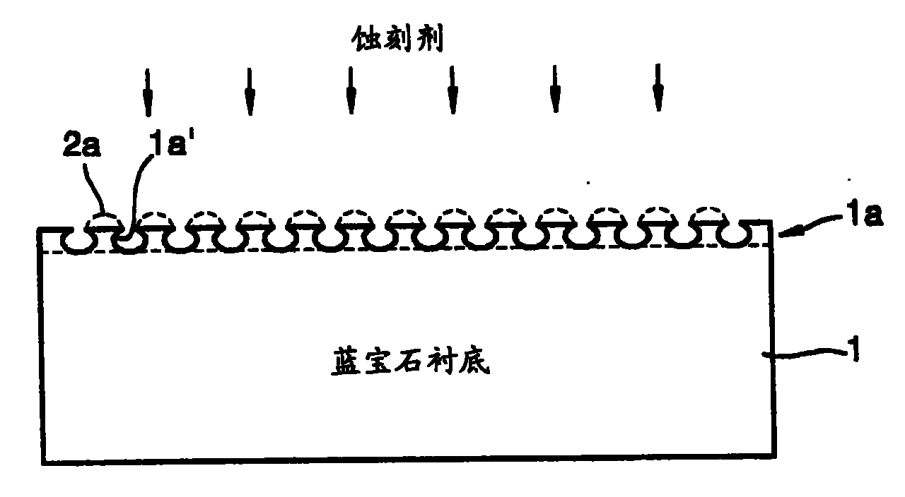
参照图1,具有纳米尺寸的点2a的掩模层2形成在准备的单晶晶片1例如Al2O3(蓝宝石)晶片(下面称为Al2O3晶片1)的表面上。掩模层2利用公知的卤化物或氢化物气相外延(HVPE)工艺形成。Referring to FIG. 1, a
具体地,Al2O3晶片1装入水平HVPE反应器(horizontal HVPE reactor)中,反应器的初始温度上升至约1050℃的生长温度。其后,HCl和NH3气体与N2气体以1∶10的比例混合,该混合物被注入到反应器中约5分钟,使得AlN点2a形成在Al2O3晶片1上。之后,反应器冷却至室温,Al2O3晶片1从反应器中取出。Specifically, the Al 2 O 3
该工艺中,纳米尺寸的点2a形成在其上的Al2O3晶片1的表面粗糙度从数

参照图2,多孔缓冲层1a利用蚀刻工艺形成在Al2O3晶片1上。为了形成多孔缓冲层1a,采用对于Al2O3晶片1比掩模层2具有更高溶解度的蚀刻剂。因此,未覆盖有点2a的部分Al2O3晶片1被高速蚀刻,而掩模层2被低速蚀刻。蚀刻工艺持续进行直到掩模层2被完全除去且孔1a′形成至数十nm的直径和深度。结果,如图2所示,具有纳米尺寸的孔1a′的多孔缓冲层1a形成在Al2O3晶片1的表面上。Referring to FIG. 2, a
参照图3,所需外延材料层3利用常见外延生长工艺形成在缓冲层1a上。例如,为了利用III族氮化物半导体形成外延材料层3,Al2O3晶片1被装入HVPE反应器中,发生HCl和Ga之间的反应,因此产生GaCl,且发生GaCl和NH3之间的反应,因此在Al2O3晶片1的表面上生长GaN外延材料层3至数μm的厚度。该外延生长工艺期间,控制工艺条件使得水平方向测量的外延生长速率高于垂直方向测量的外延生长速率。Referring to FIG. 3 , the required
一旦外延生长工艺完成,就将HVPE反应器冷却到室温,从HVPE反应器中取出GaN半导体外延材料层3生长在其上的Al2O3晶片1。Once the epitaxial growth process is completed, the HVPE reactor is cooled to room temperature, and the Al 2 O 3 wafer 1 on which the GaN semiconductor
参照图4,外延材料层3利用快速热退火(RTA)工艺退火。对于该工艺,Al2O3晶片1装入维持在NH3气氛中的炉中然后在850℃或者更高的温度退火。Referring to FIG. 4, the
通过上述工艺,所需的外延材料层3形成在Al2O3晶片1上。Through the above process, the required
当GaN外延材料层通过上述工艺实际形成时,得到下面的测量数据。即,该GaN外延材料层具有约5×10⁷/cm2的缺陷密度,其小于5×109/cm2的传统缺陷密度,且具有传统GaN层的张应力(strain stress)的约1/5。When the GaN epitaxial material layer was actually formed through the above process, the following measurement data were obtained. That is, the GaN epitaxial material layer has a defect density of about 5×10 7 /cm 2 , which is smaller than the conventional defect density of 5×10 9 /cm 2 , and has about 1/3 the strain stress of the conventional GaN layer. 5.
可选器件可直接形成在已经经历上述工艺的晶片1上。作为替代地,为了得到独立的(freestanding)GaN晶片,Al2O3晶片1可再次装入HVPE反应器中且另一GaN外延材料层可进一步生长在GaN外延材料层3上至约300μm或更大的厚度。随后,Al2O3晶片1可利用公知的激光顶离工艺(laserlift-offprocess)取下,从而得到具有约5×10⁵/cm2的缺陷密度的高质量独立式GaN晶片。Alternative devices can be formed directly on the
图5是通过本发明的方法得到的具有AlN点的Al2O3晶片的扫描电子显微镜(SEM)图像。形成AlN点之前测量的Al2O3晶片的表面粗糙度是3.16而形成AlN点之后测量的Al2O3晶片的表面粗糙度是21.3
根据本发明,多孔缓冲层利用蚀刻工艺形成在单晶晶片上。特别地,形成掩模层从而由于晶片的表面反应而得到多孔缓冲层。因为多孔缓冲层利用蚀刻工艺形成,晶片可由很多种材料形成。According to the present invention, a porous buffer layer is formed on a single crystal wafer using an etching process. In particular, a mask layer is formed to obtain a porous buffer layer due to the surface reaction of the wafer. Because the porous buffer layer is formed using an etching process, the wafer can be formed from a wide variety of materials.
另外,本发明减小了缺陷密度、应力、以及外延生长衬底的弯曲度,因此能够形成高质量半导体晶片且提高合格率。此外,由于上述物理属性的改善,可以制造具有较大直径的外延生长半导体晶片。In addition, the present invention reduces defect density, stress, and curvature of the epitaxial growth substrate, so high-quality semiconductor wafers can be formed and the yield can be improved. In addition, due to the improvement of the above-mentioned physical properties, epitaxially grown semiconductor wafers having larger diameters can be manufactured.
另外,本发明适于单晶半导体晶片,其依赖地形成在另一衬底上,例如,III族氮化物半导体晶片诸如GaN晶片。In addition, the present invention is suitable for a single crystal semiconductor wafer which is dependently formed on another substrate, for example, a Group III nitride semiconductor wafer such as a GaN wafer.
虽然参考本发明的示例性实施例特别显示和说明了本发明,但是本领域普通技术人员应理解的是,在不偏离后附权利要求所定义的本发明的思想和范围的情况下,可进行形式和细节上的各种改变。Although the present invention has been particularly shown and described with reference to exemplary embodiments of the present invention, it should be understood by those skilled in the art that, without departing from the spirit and scope of the present invention as defined by the appended claims, various Various changes in form and detail.
Claims (9)
Applications Claiming Priority (2)
| Application Number | Priority Date | Filing Date | Title |
|---|---|---|---|
| KR1020050001540A KR100682879B1 (en) | 2005-01-07 | 2005-01-07 | Crystal growth method |
| KR1540/05 | 2005-01-07 |
Publications (2)
| Publication Number | Publication Date |
|---|---|
| CN1812053A CN1812053A (en) | 2006-08-02 |
| CN100418191C true CN100418191C (en) | 2008-09-10 |
Family
ID=36652408
Family Applications (1)
| Application Number | Title | Priority Date | Filing Date |
|---|---|---|---|
| CNB2005101316159A Expired - Fee Related CN100418191C (en) | 2005-01-07 | 2005-12-15 | epitaxial growth method |
Country Status (4)
| Country | Link |
|---|---|
| US (2) | US20060151797A1 (en) |
| JP (1) | JP5469792B2 (en) |
| KR (1) | KR100682879B1 (en) |
| CN (1) | CN100418191C (en) |
Cited By (1)
| Publication number | Priority date | Publication date | Assignee | Title |
|---|---|---|---|---|
| CN106397225A (en) * | 2016-09-04 | 2017-02-15 | 王际菊 | Preparation method of chiral compound |
Families Citing this family (28)
| Publication number | Priority date | Publication date | Assignee | Title |
|---|---|---|---|---|
| KR100695117B1 (en) * | 2005-10-25 | 2007-03-14 | 삼성코닝 주식회사 | Manufacturing method |
| GB0701069D0 (en) * | 2007-01-19 | 2007-02-28 | Univ Bath | Nanostructure template and production of semiconductors using the template |
| GB0702560D0 (en) * | 2007-02-09 | 2007-03-21 | Univ Bath | Production of Semiconductor devices |
| KR100878512B1 (en) * | 2007-05-14 | 2009-01-13 | 나이넥스 주식회사 | BANN semiconductor substrate manufacturing method |
| WO2008146699A1 (en) * | 2007-05-25 | 2008-12-04 | Tohoku University | Method for manufacturing gan-based nitride semiconductor self-supporting substrate |
| JP4672753B2 (en) * | 2007-05-25 | 2011-04-20 | エー・イー・テック株式会社 | GaN-based nitride semiconductor free-standing substrate manufacturing method |
| CN101409229B (en) * | 2007-10-12 | 2012-01-04 | 台达电子工业股份有限公司 | Epitaxial substrate and method for manufacturing light emitting diode device |
| CA2712148C (en) * | 2008-01-16 | 2012-08-07 | National University Corporation Tokyo University Of Agriculture And Tech Nology | Method for producing a laminated body having a1-based group-iii nitride single crystal layer, laminated body produced by the method, method for producing a1-based group-iii nitride single crystal substrate employing the laminated body, and aluminum nitride single crystal substrate |
| JP5324110B2 (en) * | 2008-01-16 | 2013-10-23 | 国立大学法人東京農工大学 | Laminated body and method for producing the same |
| KR100990639B1 (en) | 2008-05-19 | 2010-10-29 | 삼성엘이디 주식회사 | Wafer Manufacturing Method |
| US8481411B2 (en) | 2009-06-10 | 2013-07-09 | Seoul Opto Device Co., Ltd. | Method of manufacturing a semiconductor substrate having a cavity |
| US8860183B2 (en) | 2009-06-10 | 2014-10-14 | Seoul Viosys Co., Ltd. | Semiconductor substrate, semiconductor device, and manufacturing methods thereof |
| KR101220433B1 (en) | 2009-06-10 | 2013-02-04 | 서울옵토디바이스주식회사 | Semiconductor substarte, method of fabricating the same, semiconductor device and method of fabricating the same |
| KR101106149B1 (en) * | 2009-08-26 | 2012-01-20 | 서울옵토디바이스주식회사 | Semiconductor substrate manufacturing method and light emitting device manufacturing method |
| CN104795314B (en) * | 2009-08-26 | 2018-02-09 | 首尔伟傲世有限公司 | The method for manufacturing light-emitting device |
| JP5570838B2 (en) | 2010-02-10 | 2014-08-13 | ソウル バイオシス カンパニー リミテッド | Semiconductor substrate, manufacturing method thereof, semiconductor device and manufacturing method thereof |
| CN102263175A (en) * | 2010-05-26 | 2011-11-30 | 北京北方微电子基地设备工艺研究中心有限责任公司 | LED (light-emitting diode) substrate and manufacturing method thereof |
| US8980730B1 (en) | 2010-09-14 | 2015-03-17 | Stc.Unm | Selective nanoscale growth of lattice mismatched materials |
| TWI515780B (en) * | 2011-09-21 | 2016-01-01 | 中美矽晶製品股份有限公司 | Wafer processing method |
| CN103011066B (en) * | 2011-09-21 | 2014-03-19 | 叶哲良 | Chip |
| TWI473283B (en) | 2011-09-21 | 2015-02-11 | 國立清華大學 | Wafer |
| KR101420265B1 (en) * | 2011-10-21 | 2014-07-21 | 주식회사루미지엔테크 | Method of manufacturing a substrate |
| CN103247724B (en) * | 2012-02-08 | 2016-04-20 | 郭磊 | A kind of semiconductor structure and forming method thereof |
| CN103247516B (en) * | 2012-02-08 | 2016-04-06 | 郭磊 | A kind of semiconductor structure and forming method thereof |
| CN103378227A (en) * | 2012-04-27 | 2013-10-30 | 南亚光电股份有限公司 | Method for forming patterned sapphire substrate |
| CN203787451U (en) * | 2012-08-28 | 2014-08-20 | 璨圆光电股份有限公司 | Compound semiconductor element |
| KR102311677B1 (en) | 2014-08-13 | 2021-10-12 | 삼성전자주식회사 | Semiconductor device and method of manufacturing the same |
| KR102386031B1 (en) * | 2019-12-31 | 2022-04-12 | 유영조 | Crystal growth method |
Citations (4)
| Publication number | Priority date | Publication date | Assignee | Title |
|---|---|---|---|---|
| US4032370A (en) * | 1976-02-11 | 1977-06-28 | International Audio Visual, Inc. | Method of forming an epitaxial layer on a crystalline substrate |
| US5445897A (en) * | 1989-11-22 | 1995-08-29 | Mitsubishi Kasei Polytec Company | Epitaxial wafer and process for producing the same |
| CN1240304A (en) * | 1998-06-18 | 2000-01-05 | 住友电气工业株式会社 | GaN monocrystal substrate and making method thereof |
| CN1303517A (en) * | 1998-05-29 | 2001-07-11 | 奥斯兰姆奥普托半导体股份有限两合公司 | Method for producing semiconductor elements |
Family Cites Families (16)
| Publication number | Priority date | Publication date | Assignee | Title |
|---|---|---|---|---|
| JPH07202164A (en) * | 1993-12-28 | 1995-08-04 | Furukawa Electric Co Ltd:The | Manufacturing method of semiconductor fine structure |
| US6579359B1 (en) * | 1999-06-02 | 2003-06-17 | Technologies And Devices International, Inc. | Method of crystal growth and resulted structures |
| JP2001122693A (en) * | 1999-10-22 | 2001-05-08 | Nec Corp | Base substrate for crystal growth and method of manufacturing substrate using the same |
| JP2002161000A (en) * | 2000-11-22 | 2002-06-04 | Otts:Kk | Method for producing gallium nitride single crystal |
| JP4015849B2 (en) * | 2001-01-29 | 2007-11-28 | 松下電器産業株式会社 | Manufacturing method of nitride semiconductor substrate |
| JP2004059325A (en) * | 2001-07-04 | 2004-02-26 | Fuji Photo Film Co Ltd | Method for manufacturing substrate for semiconductor device, substrate for semiconductor device, and semiconductor device |
| JP2003022973A (en) * | 2001-07-06 | 2003-01-24 | Sanyo Electric Co Ltd | Nitride system semiconductor device and method of forming it |
| JP3785970B2 (en) * | 2001-09-03 | 2006-06-14 | 日本電気株式会社 | Method for manufacturing group III nitride semiconductor device |
| JP4131101B2 (en) * | 2001-11-28 | 2008-08-13 | 日亜化学工業株式会社 | Method of manufacturing nitride semiconductor device |
| JP4331906B2 (en) * | 2001-12-26 | 2009-09-16 | 日本碍子株式会社 | Method for producing group III nitride film |
| JP4088111B2 (en) | 2002-06-28 | 2008-05-21 | 日立電線株式会社 | Porous substrate and manufacturing method thereof, GaN-based semiconductor multilayer substrate and manufacturing method thereof |
| US7176115B2 (en) * | 2003-03-20 | 2007-02-13 | Matsushita Electric Industrial Co., Ltd. | Method of manufacturing Group III nitride substrate and semiconductor device |
| JP2007534146A (en) * | 2003-09-05 | 2007-11-22 | ザ・ユニバーシティ・オブ・ノース・カロライナ・アット・シャーロット | Quantum dot optoelectronic device epitaxially grown in nanoscale and method for manufacturing the same |
| KR20050051169A (en) | 2003-11-27 | 2005-06-01 | 엄장필 | Method for disk allocation in mail system |
| KR100576854B1 (en) * | 2003-12-20 | 2006-05-10 | 삼성전기주식회사 | Nitride semiconductor manufacturing method and nitride semiconductor using same |
| JP2005202164A (en) | 2004-01-15 | 2005-07-28 | Omron Corp | Optical fiber holding member and manufacturing method thereof |
-
2005
- 2005-01-07 KR KR1020050001540A patent/KR100682879B1/en not_active Expired - Fee Related
- 2005-12-15 CN CNB2005101316159A patent/CN100418191C/en not_active Expired - Fee Related
- 2005-12-27 JP JP2005376483A patent/JP5469792B2/en not_active Expired - Fee Related
-
2006
- 2006-01-06 US US11/326,172 patent/US20060151797A1/en not_active Abandoned
-
2009
- 2009-03-13 US US12/382,329 patent/US8475588B2/en not_active Expired - Fee Related
Patent Citations (4)
| Publication number | Priority date | Publication date | Assignee | Title |
|---|---|---|---|---|
| US4032370A (en) * | 1976-02-11 | 1977-06-28 | International Audio Visual, Inc. | Method of forming an epitaxial layer on a crystalline substrate |
| US5445897A (en) * | 1989-11-22 | 1995-08-29 | Mitsubishi Kasei Polytec Company | Epitaxial wafer and process for producing the same |
| CN1303517A (en) * | 1998-05-29 | 2001-07-11 | 奥斯兰姆奥普托半导体股份有限两合公司 | Method for producing semiconductor elements |
| CN1240304A (en) * | 1998-06-18 | 2000-01-05 | 住友电气工业株式会社 | GaN monocrystal substrate and making method thereof |
Cited By (1)
| Publication number | Priority date | Publication date | Assignee | Title |
|---|---|---|---|---|
| CN106397225A (en) * | 2016-09-04 | 2017-02-15 | 王际菊 | Preparation method of chiral compound |
Also Published As
| Publication number | Publication date |
|---|---|
| CN1812053A (en) | 2006-08-02 |
| JP2006191074A (en) | 2006-07-20 |
| JP5469792B2 (en) | 2014-04-16 |
| KR20060081107A (en) | 2006-07-12 |
| KR100682879B1 (en) | 2007-02-15 |
| US20090181525A1 (en) | 2009-07-16 |
| US20060151797A1 (en) | 2006-07-13 |
| US8475588B2 (en) | 2013-07-02 |
Similar Documents
| Publication | Publication Date | Title |
|---|---|---|
| CN100418191C (en) | epitaxial growth method | |
| CN100530543C (en) | Epitaxial growth method | |
| JP5135501B2 (en) | Manufacturing method of nitride single crystal substrate and manufacturing method of nitride semiconductor light emitting device using the same | |
| US7708832B2 (en) | Method for preparing substrate for growing gallium nitride and method for preparing gallium nitride substrate | |
| EP2333817B1 (en) | Method for preparing compound semiconductor substrate | |
| JP2002343728A (en) | Gallium nitride crystal substrate manufacturing method and gallium nitride crystal substrate | |
| US7435666B2 (en) | Epitaxial growth method | |
| US8591652B2 (en) | Semi-conductor substrate and method of masking layer for producing a free-standing semi-conductor substrate by means of hydride-gas phase epitaxy | |
| US7696071B2 (en) | Group III nitride based semiconductor and production method therefor | |
| JP4665286B2 (en) | Semiconductor substrate and manufacturing method thereof | |
| JP2001200366A (en) | Method for producing crack-free gallium nitride thick film by hydride vapor phase epitaxy | |
| CN111052306B (en) | Substrate and preparation method thereof | |
| KR20170011932A (en) | Method for self-separation and fabrication of low defect nitride semiconductor substrate by using chemical vapor etching technique | |
| KR20160063796A (en) | Method of GaN wafer manufacturing for minimization of wafer bowing and cracking | |
| JP2007277062A (en) | Group III nitride crystal substrate manufacturing method and group III nitride crystal substrate |
Legal Events
| Date | Code | Title | Description |
|---|---|---|---|
| C06 | Publication | ||
| PB01 | Publication | ||
| C10 | Entry into substantive examination | ||
| SE01 | Entry into force of request for substantive examination | ||
| C14 | Grant of patent or utility model | ||
| GR01 | Patent grant | ||
| C56 | Change in the name or address of the patentee |
Owner name: SUMSUNG KANGNING PRECISION MATERIAL CO., LTD. Free format text: FORMER NAME: SAMSUNG CORNING PRECISION GLASS |
|
| CP03 | Change of name, title or address |
Address after: Gyeongbuk, South Korea Patentee after: Samsung Corning Precision Materials Co., Ltd. Address before: South Korea Gyeongbuk Gumi Patentee before: Samsung Corning Precision Glass |
|
| CF01 | Termination of patent right due to non-payment of annual fee |
Granted publication date: 20080910 Termination date: 20151215 |
|
| EXPY | Termination of patent right or utility model |