CN100417985C - Liquid crystal display device - Google Patents
Liquid crystal display device Download PDFInfo
- Publication number
- CN100417985C CN100417985C CNB200410102866XA CN200410102866A CN100417985C CN 100417985 C CN100417985 C CN 100417985C CN B200410102866X A CNB200410102866X A CN B200410102866XA CN 200410102866 A CN200410102866 A CN 200410102866A CN 100417985 C CN100417985 C CN 100417985C
- Authority
- CN
- China
- Prior art keywords
- liquid crystal
- crystal board
- substrate
- backlight assembly
- display device
- Prior art date
- Legal status (The legal status is an assumption and is not a legal conclusion. Google has not performed a legal analysis and makes no representation as to the accuracy of the status listed.)
- Expired - Fee Related
Links
Images


Classifications
-
- G—PHYSICS
- G02—OPTICS
- G02F—OPTICAL DEVICES OR ARRANGEMENTS FOR THE CONTROL OF LIGHT BY MODIFICATION OF THE OPTICAL PROPERTIES OF THE MEDIA OF THE ELEMENTS INVOLVED THEREIN; NON-LINEAR OPTICS; FREQUENCY-CHANGING OF LIGHT; OPTICAL LOGIC ELEMENTS; OPTICAL ANALOGUE/DIGITAL CONVERTERS
- G02F1/00—Devices or arrangements for the control of the intensity, colour, phase, polarisation or direction of light arriving from an independent light source, e.g. switching, gating or modulating; Non-linear optics
- G02F1/01—Devices or arrangements for the control of the intensity, colour, phase, polarisation or direction of light arriving from an independent light source, e.g. switching, gating or modulating; Non-linear optics for the control of the intensity, phase, polarisation or colour
- G02F1/13—Devices or arrangements for the control of the intensity, colour, phase, polarisation or direction of light arriving from an independent light source, e.g. switching, gating or modulating; Non-linear optics for the control of the intensity, phase, polarisation or colour based on liquid crystals, e.g. single liquid crystal display cells
- G02F1/133—Constructional arrangements; Operation of liquid crystal cells; Circuit arrangements
- G02F1/1333—Constructional arrangements; Manufacturing methods
- G02F1/133308—Support structures for LCD panels, e.g. frames or bezels
-
- G—PHYSICS
- G02—OPTICS
- G02F—OPTICAL DEVICES OR ARRANGEMENTS FOR THE CONTROL OF LIGHT BY MODIFICATION OF THE OPTICAL PROPERTIES OF THE MEDIA OF THE ELEMENTS INVOLVED THEREIN; NON-LINEAR OPTICS; FREQUENCY-CHANGING OF LIGHT; OPTICAL LOGIC ELEMENTS; OPTICAL ANALOGUE/DIGITAL CONVERTERS
- G02F2201/00—Constructional arrangements not provided for in groups G02F1/00 - G02F7/00
- G02F2201/50—Protective arrangements
-
- G—PHYSICS
- G02—OPTICS
- G02F—OPTICAL DEVICES OR ARRANGEMENTS FOR THE CONTROL OF LIGHT BY MODIFICATION OF THE OPTICAL PROPERTIES OF THE MEDIA OF THE ELEMENTS INVOLVED THEREIN; NON-LINEAR OPTICS; FREQUENCY-CHANGING OF LIGHT; OPTICAL LOGIC ELEMENTS; OPTICAL ANALOGUE/DIGITAL CONVERTERS
- G02F2201/00—Constructional arrangements not provided for in groups G02F1/00 - G02F7/00
- G02F2201/54—Arrangements for reducing warping-twist
Landscapes
- Physics & Mathematics (AREA)
- Nonlinear Science (AREA)
- Mathematical Physics (AREA)
- Chemical & Material Sciences (AREA)
- Crystallography & Structural Chemistry (AREA)
- General Physics & Mathematics (AREA)
- Optics & Photonics (AREA)
- Liquid Crystal (AREA)
- Devices For Indicating Variable Information By Combining Individual Elements (AREA)
Abstract
A liquid crystal display device (LCD) includes a liquid crystal panel displaying an image; a transparent plate disposed on the liquid crystal panel; a support member supporting the liquid crystal panel; and a fixing member disposed on the transparent plate, the fixing member coupled with the support member to fix the liquid crystal panel and the transparent plate in place, and to protect the liquid crystal panel and the transparent plate.
Description
Technical field
The present invention relates to a kind of liquid crystal display device, more specifically, relate to a kind of liquid crystal display device that is suitable for preventing the distortion that causes by bending stress.
Background technology
At the image display device that is used for display image on screen, be extensive use of the prior art cathode ray tube (CRT).Yet because its size and weight, the use of prior art CRT is also inconvenient.
Therefore, developed frivolous flat-panel display device.Though display area is very big, flat-panel display device is very thin and can be applicable to most of places.Owing to these reasons, prior art CRT constantly is substituted by flat-panel display device.Particularly, in flat-panel display device, the high-quality resolution rate during owing to display image, liquid crystal display device (LCD) is widely accepted.Especially, when showing animation, LCD has the same fast response time with prior art CRT.
Optical anisotropy and polarizability by liquid crystal material drive LCD.Grow owing to liquid crystal molecule is thin dimensionally, so can be by applying the alignment direction that electric field is controlled liquid crystal material to liquid crystal material with directivity and polarity.Correspondingly, when having controlled alignment direction, the optical anisotropy of liquid crystal material makes light be through or be blocked according to the alignment direction of liquid crystal material.Like this, color and image are shown.
Thin film transistor (AMLCD) comprises the active component that is arranged in the pixel with matrix structure.AMLCD uses the switching characteristic of active component to control the operation of pixel, thereby has realized memory function by electrooptical effect.Simultaneously, LCD is the passive matrix displays part that self does not have light source.Therefore, LCD needs lamp, optical plate, thin layer and other suitable components.
Fig. 1 is the open cube display of prior art CRT.With reference to Fig. 1, backlight assembly provides light to liquid crystal board 120.
Ora terminalis formula backlight assembly (edge type backlight) comprising: light source 140 is used to launch light; Reflecting plate 170 is used for the upwards reflection of light from light source 140 emissions; Optical plate 160 is used to guide the light that is reflected; And scatter plate 130, be used for the light of scattering through guiding.Simultaneously, this backlight assembly also comprises lamp support 150, the light that is used for supporting light sources 140 and is launched to optical plate 160 reflections.LCD 100 also comprises top cover 110, main corbel 180 and the end cover 190 that is used to protect and support liquid crystal board 120.
Although described ora terminalis formula backlight assembly herein, the direct-type backlight assembly (direct type backlight) with a plurality of light sources that place under the liquid crystal board also is widely accepted.Recently, developed the large-scale LCD of 60 inches or bigger model.Following problem has appearred in the size increase along with LCD.
The increase of liquid crystal board size has caused putting on the extra-stress of this liquid crystal board.This stress is to be produced by the distortion of liquid crystal board, and this distortion is by interference and crooked causing between the mechanical part (for example, top cover, main corbel, end cover and other associated components).Along with this stress puts on liquid crystal board, the contact brightness irregularities in LCD, occurred, and around the marginal portion, light leak occurred.
Summary of the invention
Therefore, the invention is intended to a kind of liquid crystal display device (LCD), it has been eliminated basically by the limitation of prior art and the not enough one or more problems that caused.
An object of the present invention is to provide a kind of LCD that can keep picture quality.
Further feature of the present invention and advantage are specifically set forth in following detailed description of the invention, and it partly can become clear by this detailed description, maybe can the acquistion by practice of the present invention.By the structure of in instructions and claim and accompanying drawing, specifically noting, will realize and obtain purpose of the present invention and other advantage.
In order to realize these and other advantage and according to purpose of the present invention, as concrete enforcement and generalized description, a kind of LCD comprises: the liquid crystal board of display image; Place the transparent support plate under the described liquid crystal board with predetermined hardness; Place being used under the described transparent support plate to support the supporting component of described transparent support plate and described liquid crystal board; And placing fixation kit on the described liquid crystal board, described fixation kit and described supporting component couple, and with described liquid crystal board and described transparent support plate fix in position, and protect described liquid crystal board and described transparent support plate; And backlight assembly, described backlight assembly has optical plate, is arranged in the below of described liquid crystal board, provides light to described liquid crystal board.
On the other hand, LCD comprises: the liquid crystal board of display image; Place the transparent panel on the described liquid crystal board; Place the transparent support plate under the described liquid crystal board with predetermined hardness; Place being used under the described transparent support plate to support the supporting component of described transparent support plate and described liquid crystal board; And placing fixation kit on the described transparent panel, described fixation kit and described supporting component couple, and with described liquid crystal board, described transparent panel and described transparent support plate fix in position, and protect described liquid crystal board, described transparent panel and described transparent support plate; And backlight assembly, described backlight assembly has optical plate, is arranged in the below of described liquid crystal board, provides light to described liquid crystal board.
The general remark and the following detailed description that should be appreciated that the front all are exemplary and indicative, are intended to the invention provides further explanation for defined by the claims.
Description of drawings
Comprise accompanying drawing to provide further understanding of the present invention, accompanying drawing is introduced among the application and constitutes the application's a part, and it shows embodiments of the invention, and is used from explanation principle of the present invention with instructions one.In the accompanying drawing:
Fig. 1 is the open cube display of prior art LCD;
Fig. 2 is the concept map that the structure of the LCD of first exemplary embodiment according to the present invention is shown;
Fig. 3 is the concept map that the structure of the LCD of second exemplary embodiment according to the present invention is shown; And
Fig. 4 is the concept map that the structure of the LCD of the 3rd exemplary embodiment according to the present invention is shown.
Embodiment
Now will describe the preferred embodiments of the present invention in detail, its example is shown in the drawings.
The invention provides a kind of LCD, it is by preventing that liquid crystal board from because of bending stress causes the plate distortion, improving picture quality.Describe the preferred embodiments of the present invention in detail with reference to accompanying drawing.
Fig. 2 is the concept map that the structure of the LCD of first exemplary embodiment according to the present invention is shown.
With reference to Fig. 2, the LCD 200 of first exemplary embodiment comprises the liquid crystal board 203 that is used for display image according to the present invention, and places the transparent panel 202 on the liquid crystal board 203.LCD 200 also comprises supporting component 204 and fixation kit 201.Supporting component 204 is supporting liquid crystal board 202.Fixation kit 201 places on the transparent panel 202 and with supporting component 204 and couples, and makes liquid crystal board 203 and transparent panel 202 be secured in place and is protected.
Although not shown, LCD 200 also comprises the backlight assembly that is used for providing to liquid crystal board 203 light.In addition, backlight assembly can adopt direct-type backlight assembly or ora terminalis formula backlight assembly.Backlight assembly places under the liquid crystal board 203.
In addition, liquid crystal board 203 comprises the liquid crystal layer that is inserted between first substrate and second substrate.Can be at the top of first substrate and the attached polarization layer in bottom of second substrate.Usually, on first substrate, be formed with color-filter layer and public electrode, and on second substrate, be formed with on-off element and pixel electrode.Can use color filter to form liquid crystal board 203 in structure or TFT structure of (TOC) on color filter of (COT) on the TFT.
Simultaneously, LCD 200 of the present invention comprises the transparent panel 202 that places on the liquid crystal board 203.Outside transparent panel 202 is protected liquid crystal boards 203 and is prevented that liquid crystal board 203 is directly exposed to.At this moment, because transparent panel 202 is to be made by the material with predetermined hardness, so prevented the distortion that liquid crystal board 203 causes owing to own wt or external pressure.
According to the present invention, owing to prevented liquid crystal board 203 because the distortion that own wt or external force cause, thereby can prevent from liquid crystal board, to occur contacting brightness disproportionation.The contact brightness disproportionation is defined as, when under complete black pattern when liquid crystal board applies an external force, because the distribution of unbalanced panel weight causes initial black state to become inhomogeneous.
Along with the size increase of liquid crystal board 203, restive more this contact brightness disproportionation.Yet the present invention is intended to solve above problem by transparent panel 202 is set on liquid crystal board 203.Especially, the present invention is effective for the LCD of the liquid crystal board with 60 inches or bigger increased in size.
Simultaneously, compare with LCD with VA mode liquid crystal plate, more effective when the present invention realizes in the LCD with IPS mode liquid crystal plate.This is because of the characteristic of IPS pattern usage level electric field.IPS mode liquid crystal plate has such tendency: it is subjected to the influence of the distortion that caused by bending stress more.
According to the present invention, the transparent panel 202 with predetermined hardness places between liquid crystal board 203 and the fixation kit 201, thereby has prevented the distortion of the liquid crystal board 203 that caused by bending stress.As a result, can reduce marginal portion light leak on every side.This light leak is defined as, and light leaks to the periphery of liquid crystal board 203 because of the distortion of the liquid crystal board 203 that bending stress causes.
In addition, the present invention has improved the tolerance limit of employed liquid crystal material amount in the process of making liquid crystal board.When the design liquid crystal cells, the liquid crystal material amount is by the cell gap decision of the shape of electro-optical characteristic, tft array and the color filter array of having considered liquid crystal board inside.The interval of satisfying " amount of liquid crystal " of design conditions is known as " amount of liquid crystal " tolerance limit.
Simultaneously, under the situation that the liquid crystal board size increases, if increase amount of liquid crystal to prevent to contact brightness irregularities, then " amount of liquid crystal " tolerance limit descends.Yet the present invention can use transparent panel to solve this contact brightness irregularities.Therefore, can enlarge the interval of " amount of liquid crystal " that satisfy design conditions.
Fig. 3 is the concept map that the structure of the LCD of second exemplary embodiment according to the present invention is shown.
With reference to Fig. 3, the LCD 300 of second exemplary embodiment comprises liquid crystal board 302 that is used for display image and the transparent panel 303 that places under this liquid crystal board 302 according to the present invention.LCD 300 also comprises supporting component 304 and fixation kit 301.Supporting component 304 places under the transparent panel 303 and supports transparent panel 303 and liquid crystal board 302.In addition, fixation kit 301 places on the liquid crystal board 302.Fixation kit 301 couples with supporting component 304, makes liquid crystal board 302 and transparent panel 303 be secured in place and is protected.
Although not shown, LCD 300 also comprises the backlight assembly that is used for providing to liquid crystal board 302 light.In addition, backlight assembly can adopt direct-type backlight assembly or ora terminalis formula backlight assembly.Backlight assembly places under the liquid crystal board 302.
Although not shown, liquid crystal board 302 comprises the liquid crystal layer that is inserted between first substrate and second substrate.Can be at the top of first substrate and the attached polarization layer in bottom of second substrate.Usually, on first substrate, be formed with color-filter layer and public electrode, and on second substrate, be formed with on-off element and pixel electrode.Can use color filter to form liquid crystal board 302 in structure or TFT structure of (TOC) on color filter of (COT) on the TFT.
Simultaneously, LCD 300 of the present invention is characterised in that transparent panel 303 places under the liquid crystal board 302.Transparent panel 303 has been eliminated the mechanical clearance between supporting component 304 and the liquid crystal board 302.At this moment, because transparent panel 303 is to be made by the material with predetermined hardness, so prevented that liquid crystal board 302 is owing to weight of self or the distortion that is caused by the mechanical clearance institute applied pressure between supporting component 304 and the liquid crystal board 302.Thereby, can prevent from liquid crystal board, to occur the contact brightness disproportionation.
Along with the size increase of liquid crystal board 302, restive more this contact brightness irregularities.Yet the present invention handles above problem by transparent panel 303 is set under liquid crystal board 302.Especially, the present invention is effective for the LCD of the liquid crystal board with 60 inches or bigger increased in size.
With compare for LCD with VA mode liquid crystal plate, the present invention can provide the control of better contact brightness disproportionation for the LCD with IPS mode liquid crystal plate.This is because of the characteristic of the IPS pattern of usage level electric field, because IPS mode liquid crystal plate is subjected to the influence of the distortion that caused by bending stress more.
According to the present invention, the transparent panel 303 with predetermined hardness places between liquid crystal board 302 and the supporting component 304, thereby has prevented that liquid crystal board 302 is out of shape because of bending stress.As a result, can reduce marginal portion light leak on every side.
In addition, the present invention has improved the tolerance limit of employed liquid crystal material amount in the process of making liquid crystal board.When the design liquid crystal cells, the liquid crystal material amount is by the cell gap decision of the shape of electro-optical characteristic, tft array and the color filter array of having considered liquid crystal board inside.The interval of satisfying " amount of liquid crystal " of design conditions is known as " amount of liquid crystal " tolerance limit.
Simultaneously, for the liquid crystal board of increased in size, if increase the liquid crystal material amount with control contact brightness disproportionation, then " amount of liquid crystal " tolerance limit descends.Yet the present invention can use transparent panel to control this contact brightness disproportionation.Therefore, can enlarge the interval of " amount of liquid crystal " that satisfy design conditions.
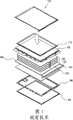
Fig. 4 shows the concept map of the structure of the LCD of the 3rd exemplary embodiment according to the present invention.
With reference to Fig. 4, the LCD 400 of the 3rd exemplary embodiment comprises according to the present invention, is used for the liquid crystal board 403 and first transparent panel 402 that places on this liquid crystal board 403 of display image, and places second transparent panel 404 under the liquid crystal board 403.LCD 400 also comprises supporting component 405 and fixation kit 401.
Supporting component 405 places under second transparent panel 404 and supports second transparent panel 404 and liquid crystal board 403.Fixation kit 401 is arranged on first transparent panel 402.Fixation kit 401 is coupled to supporting component 405, makes the liquid crystal board 403 and first transparent panel 402 and second transparent panel 404 be secured in place and is protected.
Fixation kit 401 can be top cover form or other form, and supporting component 405 can be main corbel form, end cover or other form.According to the selection of components of LCD, can change fixation kit 401 and supporting component 405 in many ways.Simultaneously, whether fixation kit 401 and supporting component 405 are suitable for according to existing the shape of backlight assembly or backlight assembly to change.
Although not shown, LCD 400 also comprises the backlight assembly that is used for providing to liquid crystal board 403 light.In addition, backlight assembly can adopt direct-type backlight assembly or ora terminalis formula backlight assembly.Selected backlight assembly places under the liquid crystal board 403.
Although not shown, liquid crystal board 403 comprises the liquid crystal layer that is inserted between first substrate and second substrate.Can be at the top of first substrate and the attached polarization layer in bottom of second substrate.Usually, on first substrate, be formed with color-filter layer and public electrode, and on second substrate, be formed with on-off element and pixel electrode.Can use color filter to form liquid crystal board 403 in structure or TFT structure of (TOC) on color filter of (COT) on the TFT.
Liquid crystal board 403 is suitable for realizing with polytype: comprise reflection-type, transmission-type and Semitransmissive.In addition, liquid crystal board 403 is suitable for to comprise that the various modes of switching (IPS) pattern and vertical orientation (VA) pattern in twisted-nematic (TN) pattern, the face realizes.
Simultaneously, LCD 400 of the present invention comprises first transparent panel 402 and second transparent panel 404 that places liquid crystal board 403 upper and lower respectively.Outside first transparent panel 402 is protected liquid crystal boards 403 and is prevented that liquid crystal board 403 is directly exposed to.At this moment, because first transparent panel 402 is to be made by the material with predetermined hardness, so prevented the distortion that liquid crystal board 403 causes owing to own wt or external pressure.
In addition, second transparent panel 404 has been eliminated the mechanical clearance between supporting component 405 and the liquid crystal board 403.Thereby, prevented that liquid crystal board 403 is owing to distortion of self or the distortion that is caused by the mechanical clearance institute applied pressure between supporting component 405 and the liquid crystal board 403.
The invention provides reliable protection more, prevent that liquid crystal board 403 from deforming.Therefore, can prevent from liquid crystal board, to occur the contact brightness disproportionation.
Along with the size increase of liquid crystal board 403, restive more this contact brightness disproportionation.Yet, the present invention can by on the liquid crystal board 403 and under first transparent panel 402 is set and second transparent panel 404 is handled above problem.Especially, the present invention is effective for the LCD of the liquid crystal board with 60 inches or bigger increased in size.
In addition, and compare for the LCD with VA mode liquid crystal plate, the present invention can provide better control for the contact brightness disproportionation of the LCD with IPS mode liquid crystal plate.This is because of the characteristic of the IPS pattern of usage level electric field, because IPS mode liquid crystal plate is subjected to the influence of the distortion that caused by bending stress more.
According to the present invention, first transparent panel 402 with predetermined hardness places between liquid crystal board 403 and the fixation kit 401, and second transparent panel 404 with predetermined hardness places between liquid crystal board 403 and the supporting component 405, thereby has prevented liquid crystal board 403 distortion.As a result, can reduce marginal portion light leak on every side.
In addition, the present invention can improve the tolerance limit of employed liquid crystal material amount in the process of making liquid crystal board.When the design liquid crystal cells, the liquid crystal material amount is by the cell gap decision of the shape of electro-optical characteristic, tft array and the color filter array of having considered liquid crystal board inside.The interval of satisfying " amount of liquid crystal " of design conditions is known as " amount of liquid crystal " tolerance limit.
Simultaneously, under the situation that the size of liquid crystal board increases, if increase amount of liquid crystal with control contact brightness disproportionation, then " amount of liquid crystal " tolerance limit descends.Yet the present invention can use transparent panel to solve this contact brightness disproportionation.Therefore, can enlarge the interval of " amount of liquid crystal " that satisfy design conditions.
As mentioned above, by preventing liquid crystal board because bending stress is out of shape, LCD according to the present invention has improved picture quality.In addition, LCD according to the present invention has reduced the contact brightness disproportionation, thereby has prevented the light leak around the marginal portion.In addition, LCD according to the present invention has enlarged " amount of liquid crystal " interval.
For those skilled in the art, clearly, under the situation that does not break away from the spirit or scope of the present invention, can carry out numerous modifications and variations to liquid crystal display device of the present invention (LCD).Therefore, the present invention is intended to cover all these modifications and variations of the present invention, as long as they fall in claims and its equivalent institute restricted portion.
Claims (10)
1. liquid crystal display device, described liquid crystal display device comprises:
The liquid crystal board of display image;
Place the transparent support plate under the described liquid crystal board with predetermined hardness;
Place being used under the described transparent support plate to support the supporting component of described transparent support plate and described liquid crystal board; And
Place the fixation kit on the described liquid crystal board, described fixation kit and described supporting component couple, and with described liquid crystal board and described transparent support plate fix in position, and protect described liquid crystal board and described transparent support plate; And
Backlight assembly, described backlight assembly has optical plate, is arranged in the below of described liquid crystal board, provides light to described liquid crystal board.
2. liquid crystal display device according to claim 1, wherein said liquid crystal board comprise at least a in twisted nematic mode, in-plane-switching mode and the vertical alignment mode.
3. liquid crystal display device according to claim 1, wherein said backlight assembly are the direct-type backlight assembly.
4. liquid crystal display device according to claim 1, wherein said backlight assembly are ora terminalis formula backlight assembly.
5. liquid crystal display device according to claim 1, wherein said liquid crystal board comprises:
First substrate;
With preset distance and described first substrate second substrate separately;
Place the liquid crystal layer between described first substrate and described second substrate;
Place first polarization layer on described first substrate; And
Place second polarization layer under described second substrate.
6. liquid crystal display device, described liquid crystal display device comprises:
The liquid crystal board of display image;
Place the transparent panel on the described liquid crystal board;
Place the transparent support plate under the described liquid crystal board with predetermined hardness;
Place being used under the described transparent support plate to support the supporting component of described transparent support plate and described liquid crystal board; And
Place the fixation kit on the described transparent panel, described fixation kit and described supporting component couple, and with described liquid crystal board, described transparent panel and described transparent support plate fix in position, and protect described liquid crystal board, described transparent panel and described transparent support plate; And
Backlight assembly, described backlight assembly has optical plate, is arranged in the below of described liquid crystal board, provides light to described liquid crystal board.
7. liquid crystal display device according to claim 6, wherein said liquid crystal board comprise at least a in twisted nematic mode, in-plane-switching mode and the vertical alignment mode.
8. liquid crystal display device according to claim 6, wherein said backlight assembly are the direct-type backlight assembly.
9. liquid crystal display device according to claim 6, wherein said backlight assembly are ora terminalis formula backlight assembly.
10. liquid crystal display device according to claim 6, wherein said liquid crystal board comprises:
First substrate;
With preset distance and described first substrate second substrate separately;
Place the liquid crystal layer between described first substrate and described second substrate;
Place first polarization layer on described first substrate; And
Place second polarization layer under described second substrate.
Applications Claiming Priority (2)
| Application Number | Priority Date | Filing Date | Title |
|---|---|---|---|
| KR1020040030383A KR100607747B1 (en) | 2004-04-30 | 2004-04-30 | LCD Display |
| KR1020040030383 | 2004-04-30 |
Publications (2)
| Publication Number | Publication Date |
|---|---|
| CN1693961A CN1693961A (en) | 2005-11-09 |
| CN100417985C true CN100417985C (en) | 2008-09-10 |
Family
ID=35186678
Family Applications (1)
| Application Number | Title | Priority Date | Filing Date |
|---|---|---|---|
| CNB200410102866XA Expired - Fee Related CN100417985C (en) | 2004-04-30 | 2004-12-24 | Liquid crystal display device |
Country Status (4)
| Country | Link |
|---|---|
| US (3) | US20050243242A1 (en) |
| JP (1) | JP2005316379A (en) |
| KR (1) | KR100607747B1 (en) |
| CN (1) | CN100417985C (en) |
Families Citing this family (7)
| Publication number | Priority date | Publication date | Assignee | Title |
|---|---|---|---|---|
| JP4282611B2 (en) * | 2005-01-13 | 2009-06-24 | Nec液晶テクノロジー株式会社 | Liquid crystal display |
| JP5315064B2 (en) * | 2007-01-31 | 2013-10-16 | セイコーインスツル株式会社 | Display device |
| JP4413935B2 (en) * | 2007-02-13 | 2010-02-10 | 株式会社 日立ディスプレイズ | Liquid crystal display |
| KR20090129805A (en) * | 2008-06-13 | 2009-12-17 | 엘지디스플레이 주식회사 | Array board for transverse electric field type liquid crystal display |
| KR101974107B1 (en) * | 2012-02-02 | 2019-05-02 | 삼성디스플레이 주식회사 | Display apparatus |
| JP2014026173A (en) * | 2012-07-27 | 2014-02-06 | Japan Display Inc | Liquid crystal display device |
| US9635305B1 (en) | 2012-11-03 | 2017-04-25 | Iontank, Ltd. | Display apparatus including a transparent electronic monitor |
Citations (5)
| Publication number | Priority date | Publication date | Assignee | Title |
|---|---|---|---|---|
| JPH09113880A (en) * | 1995-10-16 | 1997-05-02 | Alpine Electron Inc | Display device |
| CN2459575Y (en) * | 2001-01-06 | 2001-11-14 | 海尔集团公司 | Screen installation box for controller of cabinet type air conditioner |
| CN1329726A (en) * | 1998-12-09 | 2002-01-02 | 时至准钟表股份有限公司 | Liquid-crystal display device |
| US6407781B2 (en) * | 2000-03-24 | 2002-06-18 | Hitachi, Ltd. | LCD device having electronic formed within concave portion of a reflector |
| CN1416068A (en) * | 2001-10-30 | 2003-05-07 | 宏达国际电子股份有限公司 | Personal digital assistant with water and dust resistance |
Family Cites Families (23)
| Publication number | Priority date | Publication date | Assignee | Title |
|---|---|---|---|---|
| JPH0345525U (en) | 1989-09-12 | 1991-04-26 | ||
| US5150231A (en) * | 1989-12-29 | 1992-09-22 | Canon Kabushiki Kaisha | Impact resistant ferroelectric liquid crystal apparatus |
| JP2861200B2 (en) | 1990-02-20 | 1999-02-24 | 松下電器産業株式会社 | Ferroelectric liquid crystal device |
| DE69323597T2 (en) * | 1992-11-12 | 1999-08-19 | Canon K.K. | Liquid crystal display device |
| DE69423552T2 (en) * | 1993-08-10 | 2000-09-07 | Canon K.K., Tokio/Tokyo | Liquid crystal display |
| US5808707A (en) * | 1995-03-01 | 1998-09-15 | Canon Kabushiki Kaisha | Display apparatus |
| JP3215844B2 (en) * | 1995-04-18 | 2001-10-09 | キヤノン株式会社 | Display device and method of manufacturing the display device |
| JPH08286204A (en) | 1995-04-19 | 1996-11-01 | Sharp Corp | Liquid crystal display device and its production |
| JPH11305205A (en) * | 1998-04-22 | 1999-11-05 | Hitachi Ltd | Liquid crystal display |
| US6504587B1 (en) * | 1998-06-17 | 2003-01-07 | Hitachi, Ltd. | Liquid crystal display device in which the inner frame having sidewall |
| JP3331326B2 (en) * | 1998-11-13 | 2002-10-07 | 株式会社東芝 | Surface light source device and flat display device using the same |
| JP2001013876A (en) | 1999-06-29 | 2001-01-19 | Sanyo Electric Co Ltd | Production of display panel |
| JP2001150584A (en) | 1999-11-29 | 2001-06-05 | Nippon Zeon Co Ltd | Conductive substrate and display element using the same |
| HUP0203614A2 (en) | 2000-07-31 | 2003-06-28 | Koninkl Philips Electronics Nv | Image-sensing display device |
| JP3969979B2 (en) * | 2001-08-29 | 2007-09-05 | 株式会社アドバンスト・ディスプレイ | Flat panel display |
| JP3726900B2 (en) * | 2002-06-24 | 2005-12-14 | セイコーエプソン株式会社 | Display device and electronic apparatus equipped with the same |
| JP2004184861A (en) | 2002-12-05 | 2004-07-02 | Tama Electric Co Ltd | Liquid crystal display device and backlight device |
| KR20070112312A (en) * | 2006-05-20 | 2007-11-23 | 삼성전자주식회사 | Backlight Assembly and Display Device Having Same |
| JP4305486B2 (en) * | 2006-09-28 | 2009-07-29 | エプソンイメージングデバイス株式会社 | LCD panel |
| KR20080032990A (en) * | 2006-10-12 | 2008-04-16 | 삼성전자주식회사 | Backlight assembly and liquid crystal display including the same |
| KR101407622B1 (en) * | 2007-11-09 | 2014-06-13 | 삼성디스플레이 주식회사 | Display device |
| KR101274153B1 (en) * | 2008-04-21 | 2013-06-13 | 엘지디스플레이 주식회사 | Liquid crystal display device |
| JP2009265366A (en) * | 2008-04-25 | 2009-11-12 | Sharp Corp | Liquid crystal display device |
-
2004
- 2004-04-30 KR KR1020040030383A patent/KR100607747B1/en active IP Right Grant
- 2004-12-24 CN CNB200410102866XA patent/CN100417985C/en not_active Expired - Fee Related
- 2004-12-27 US US11/020,172 patent/US20050243242A1/en not_active Abandoned
- 2004-12-28 JP JP2004380205A patent/JP2005316379A/en active Pending
-
2008
- 2008-01-10 US US12/007,436 patent/US7868966B2/en not_active Expired - Lifetime
-
2011
- 2011-01-10 US US12/987,818 patent/US8692952B2/en not_active Expired - Fee Related
Patent Citations (5)
| Publication number | Priority date | Publication date | Assignee | Title |
|---|---|---|---|---|
| JPH09113880A (en) * | 1995-10-16 | 1997-05-02 | Alpine Electron Inc | Display device |
| CN1329726A (en) * | 1998-12-09 | 2002-01-02 | 时至准钟表股份有限公司 | Liquid-crystal display device |
| US6407781B2 (en) * | 2000-03-24 | 2002-06-18 | Hitachi, Ltd. | LCD device having electronic formed within concave portion of a reflector |
| CN2459575Y (en) * | 2001-01-06 | 2001-11-14 | 海尔集团公司 | Screen installation box for controller of cabinet type air conditioner |
| CN1416068A (en) * | 2001-10-30 | 2003-05-07 | 宏达国际电子股份有限公司 | Personal digital assistant with water and dust resistance |
Also Published As
| Publication number | Publication date |
|---|---|
| CN1693961A (en) | 2005-11-09 |
| KR100607747B1 (en) | 2006-08-01 |
| US20110102703A1 (en) | 2011-05-05 |
| US7868966B2 (en) | 2011-01-11 |
| US8692952B2 (en) | 2014-04-08 |
| US20080129919A1 (en) | 2008-06-05 |
| US20050243242A1 (en) | 2005-11-03 |
| KR20050104927A (en) | 2005-11-03 |
| JP2005316379A (en) | 2005-11-10 |
Similar Documents
| Publication | Publication Date | Title |
|---|---|---|
| US7663715B2 (en) | Back light assembly and tiled display device having the same | |
| US7077542B2 (en) | Backlight assembly and liquid crystal display device using the same | |
| US7465062B2 (en) | Backlight assembly with supporting member and display device having the same | |
| US20080291354A1 (en) | Liquid crystal display device | |
| US8692952B2 (en) | Liquid crystal display device having a transparent plate disposed on both sides of the liquid crystal panel | |
| KR20060015174A (en) | Prism sheet and liquid crystal display device having same | |
| KR20060021558A (en) | Liquid Crystal Display Improves Bottom Chassis | |
| US20060044837A1 (en) | Backlight assembly provided with an improved light guiding plate and a display device provided with the same | |
| US8325294B2 (en) | Backlight unit including lamp guide | |
| KR100504539B1 (en) | Liquid Crystal Display Device | |
| US20080284937A1 (en) | Liquid crystal display and manufacturing method thereof | |
| KR100975750B1 (en) | Dual LCD with Dual Front Lights | |
| KR20070066218A (en) | Backlight Assembly and Liquid Crystal Display Using Same | |
| KR100239746B1 (en) | Back-light apparatus which has improved a visual angle and a LCD using the same | |
| KR20080047198A (en) | LCD Display | |
| KR100843477B1 (en) | Dual LCD with Dual Front Lights | |
| KR100989248B1 (en) | Dual LCD with Dual Front Lights | |
| KR101211299B1 (en) | Backiligt Unit and Liquid Cristal Display Device using the same | |
| KR20120121584A (en) | Liquid crystal display device | |
| KR20100044026A (en) | Liquid crystal display device | |
| US10754087B2 (en) | Guide panel, backlight unit and liquid crystal display device including the same | |
| KR20070015696A (en) | Top chassis and display device having the same | |
| KR100972498B1 (en) | LCD display device | |
| KR20050063562A (en) | Liquid crystal display module | |
| KR20070060268A (en) | Desktop calendar with liquid crystal display |
Legal Events
| Date | Code | Title | Description |
|---|---|---|---|
| C06 | Publication | ||
| PB01 | Publication | ||
| C10 | Entry into substantive examination | ||
| SE01 | Entry into force of request for substantive examination | ||
| C14 | Grant of patent or utility model | ||
| GR01 | Patent grant | ||
| CF01 | Termination of patent right due to non-payment of annual fee |
Granted publication date: 20080910 Termination date: 20211224 |
|
| CF01 | Termination of patent right due to non-payment of annual fee |