CN100409682C - Image signal processing circuit, image display device and display drive device - Google Patents
Image signal processing circuit, image display device and display drive device Download PDFInfo
- Publication number
- CN100409682C CN100409682C CNB2005100669524A CN200510066952A CN100409682C CN 100409682 C CN100409682 C CN 100409682C CN B2005100669524 A CNB2005100669524 A CN B2005100669524A CN 200510066952 A CN200510066952 A CN 200510066952A CN 100409682 C CN100409682 C CN 100409682C
- Authority
- CN
- China
- Prior art keywords
- processing circuit
- signal processing
- image signal
- vertical
- scaler
- Prior art date
- Legal status (The legal status is an assumption and is not a legal conclusion. Google has not performed a legal analysis and makes no representation as to the accuracy of the status listed.)
- Expired - Fee Related
Links
Images


Landscapes
- Liquid Crystal Display Device Control (AREA)
- Transforming Electric Information Into Light Information (AREA)
- Television Systems (AREA)
- Control Of Indicators Other Than Cathode Ray Tubes (AREA)
- Controls And Circuits For Display Device (AREA)
Abstract
本发明提供一种在尺度转换中,可以减小电路规模且可减少垂直分辨率的劣化的图像信号处理电路。垂直定标器具有增加输入图像信号的扫描线数的功能。其增加率是1.0左右。在单位输出行数为M、单位输入行数为N、增加率为α的情况下,满足0<α<2的条件。即,α是1.0左右。多倍化电路对输入的图像信号以三倍时钟进行读出。另外,多倍化电路构成为不选择通过地址超越而读出的图像信号。水平定标器使水平方向的点数对应于液晶面板的水平像素数来进行内插。
The present invention provides an image signal processing circuit that can reduce the circuit scale and reduce the degradation of vertical resolution during scale conversion. The vertical scaler has a function of increasing the number of scanning lines of an input image signal. The increase rate thereof is about 1.0. When the number of output lines per unit is M, the number of input lines per unit is N, and the increase rate is α, the condition of 0<α<2 is satisfied. That is, α is about 1.0. The multiplexing circuit reads out the input video signal at a triple clock. In addition, the multiplexing circuit is configured not to select an image signal read out by address override. The horizontal scaler makes the number of dots in the horizontal direction correspond to the number of horizontal pixels of the liquid crystal panel for interpolation.
Description
技术领域 technical field
本发明涉及用于尺度转换图像信号后驱动显示器等的图像信号处理电路、图像显示装置和显示器驱动装置。The present invention relates to an image signal processing circuit, an image display device, and a display drive device for driving a display after scaling an image signal.
背景技术 Background technique
例如,对于液晶面板的像素数,存在VGA、XGA、WXGA等标准。VGA面板的分辨率是垂直480行/水平640点,XGA中是垂直768行/水平1024点。另一方面,图像信号有NTSC和PAL等。NTSC的情况下,分辨率是垂直240行/水平720点。因此,在由所述图像信号来驱动液晶面板的情况下,需要将其水平像素数和垂直像素数转换(尺度转换)为符合液晶面板的分辨率。For example, regarding the number of pixels of a liquid crystal panel, there are standards such as VGA, XGA, and WXGA. The resolution of the VGA panel is 480 vertical lines/horizontal 640 points, and in XGA it is vertical 768 lines/horizontal 1024 points. On the other hand, image signals include NTSC, PAL, and the like. In the case of NTSC, the resolution is 240 vertical lines/720 horizontal dots. Therefore, when the liquid crystal panel is driven by the image signal, it is necessary to convert (scale conversion) the number of horizontal pixels and the number of vertical pixels thereof to conform to the resolution of the liquid crystal panel.
作为尺度转换方法,有将480行的隔行信号暂时上变换为480P(逐行)后,使用垂直方向的定标器(scaler)使扫描线数目增加到面板的分辨率的方法(参照特开平5-252486号公报)。对于水平方向,使用通常的内插滤波器,而使水平像素数增加到规定的面板水平分辨率。As a scaling method, there is a method of temporarily up-converting a 480-line interlaced signal to 480P (progressive), and then using a vertical scaler (scaler) to increase the number of scanning lines to the resolution of the panel (see JP-A-5 -252486 Bulletin). For the horizontal direction, conventional interpolation filters are used, and the number of horizontal pixels is increased to the specified horizontal resolution of the panel.
在现有的尺度转换方法中,为了将480行的隔行信号上变换为480P的信号,使用了运动自适应型依次扫描转换,但是该转换需要大容量的存储器和复杂的信号处理电路。另外,在该转换中,由于在运动部分中,进行平均上一扫描线信息和下一扫描线信息的依次扫描,所以在静止图像中得到了良好的图像质量,但在运动部分中,成为垂直分辨率下降到一半的图像,图像质量大大劣化。In the existing scaling method, in order to up-convert the 480-line interlaced signal into a 480P signal, a motion-adaptive sequential scan conversion is used, but this conversion requires a large-capacity memory and a complex signal processing circuit. In addition, in this conversion, since in the moving part, the sequential scanning of the average previous scanning line information and the next scanning line information is performed, so good image quality is obtained in the still image, but in the moving part, it becomes vertical For images whose resolution drops to half, the image quality is greatly degraded.
另一方面,作为用小的电路规模来进行尺度转换的方法,有使用垂直方向的内插滤波器,对1半帧240行的图像信号,将其扫描线数目增加到液晶面板的行数的方法。但是,在该方法中,由于垂直方向增加率大,所以垂直分辨率产生了大的劣化。On the other hand, as a method of performing scale conversion with a small circuit size, there is a method of increasing the number of scanning lines to the number of lines of a liquid crystal panel for an image signal of 240 lines in one field using a vertical interpolation filter. method. However, in this method, since the rate of increase in the vertical direction is large, the vertical resolution is greatly deteriorated.
发明内容 Contents of the invention
本发明鉴于上述问题,其目的是提供一种可以减小电路规模且可以减少垂直分辨率的劣化的图像信号处理电路、图像显示装置和显示驱动装置。SUMMARY OF THE INVENTION In view of the above problems, an object of the present invention is to provide an image signal processing circuit, an image display device, and a display drive device that can reduce the circuit scale and reduce the degradation of vertical resolution.
本发明的图像信号处理电路为了解决上述问题,是一种尺度转换图像信号的图像信号处理电路,其特征在于,包括:垂直定标器,其将相对于所述图像信号的垂直方向的行数增加率α设定为0<α<2,并在一个水平期间中一次或多次读出所述图像信号的同一行;和多倍化电路,其构成为以多倍的时钟进行读出,并且不选择因地址超越而读出的图像信号,从约0.66到约1.58的范围中选择垂直定标器的垂直方向的行数增加率。In order to solve the above-mentioned problems, the image signal processing circuit of the present invention is an image signal processing circuit for scaling image signals, which is characterized in that it includes: a vertical scaler, which converts the number of lines in the vertical direction relative to the image signal the increase rate α is set to 0<α<2, and the same line of the image signal is read out one or more times in one horizontal period; and a multiplexing circuit configured to read out with multiple clocks, And the image signal read out due to address override is not selected, and the increase rate of the line number in the vertical direction of the vertical scaler is selected from the range of about 0.66 to about 1.58.
本发明的图像信号处理电路,其中尺度转换图像信号,其特征在于,包括:读出电路,其在一水平期间中一次或多次读出所述图像信号的同一行;垂直定标器,其将相对于经所述读出电路得到的图像信号的垂直方向的行数增加率α设定为0<α<2;和多倍化电路,其构成为以多倍的时钟进行读出,并且不选择因地址超越而读出的图像信号,从约0.66到约1.58的范围中选择垂直定标器的垂直方向的行数增加率。The image signal processing circuit of the present invention, wherein the scale conversion image signal is characterized in that it includes: a readout circuit, which reads out the same line of the image signal one or more times in a horizontal period; a vertical scaler, which setting the increase rate α of the number of lines in the vertical direction with respect to the image signal obtained through the readout circuit to be 0<α<2; and a multiplexing circuit configured to perform readout with multiple clocks, and The image signal read out due to address override is not selected, and the increase rate of the line number in the vertical direction of the vertical scaler is selected from the range of about 0.66 to about 1.58.
在这样构成的图像信号处理电路中,也可具有水平定标器,其转换相对于所述图像信号的水平方向的点数。另外,也可从约0.66到约1.58的范围中选择垂直定标器的垂直方向的行数增加率。The image signal processing circuit configured in this way may also include a horizontal scaler that converts the number of dots in the horizontal direction with respect to the image signal. In addition, the rate of increase in the number of lines in the vertical direction of the vertical scaler may also be selected from a range of about 0.66 to about 1.58.
另外,本发明的图像显示装置,其特征在于:包括上述之一的图像信号处理电路,构成为将来自该图像信号处理电路的输出图像信号供给到保持型显示面板,上述保持型显示面板是液晶面板。In addition, the image display device of the present invention is characterized in that it includes one of the image signal processing circuits described above, and is configured to supply an output image signal from the image signal processing circuit to a hold-type display panel, and the hold-type display panel is a liquid crystal display panel. panel.
本发明的显示器驱动装置为了解决上述问题,是一种尺度转换图像信号后驱动显示器的显示器驱动装置,其特征在于,包括:垂直定标器,其将相对于所述图像信号的垂直方向的行数增加率α设定为0<α≤1.2;定时控制器,其将经所述垂直定标器得到的图像信号的同一行同时写入显示器的一行或多行中。In order to solve the above-mentioned problems, the display driving device of the present invention is a display driving device that drives a display after scale-converting an image signal, and is characterized in that it includes: The number increase rate α is set to 0<α≤1.2; the timing controller writes the same line of the image signal obtained by the vertical scaler into one or more lines of the display at the same time.
在上述结构的显示其驱动装置中,也可具有水平定标器,其使相对于所述图像信号的水平方向的点数对应于所述显示器的水平像素数来进行转换。另外,也可从约0.66到约1.58的范围中选择垂直定标器的垂直方向的行数增加率。另外,所述显示器是液晶面板等保持型显示面板。In the display drive device configured as above, a horizontal scale may be provided for converting the number of dots in the horizontal direction with respect to the image signal to correspond to the number of horizontal pixels of the display. In addition, the rate of increase in the number of lines in the vertical direction of the vertical scaler may also be selected from a range of about 0.66 to about 1.58. In addition, the display is a holding type display panel such as a liquid crystal panel.
根据本发明,在尺度转换中,实现了可减小电路规模且可减轻垂直分辨率的劣化的效果。According to the present invention, in the scale conversion, the effect that the circuit scale can be reduced and the degradation of the vertical resolution can be alleviated is achieved.
附图说明 Description of drawings
图1是表示本发明的实施方式的图像显示装置和图像信号处理电路的框图;1 is a block diagram showing an image display device and an image signal processing circuit according to an embodiment of the present invention;
图2是表示垂直定标器的一例的说明图;FIG. 2 is an explanatory diagram showing an example of a vertical scaler;
图3是表示图2的垂直定标器的输入和输出的关系的说明图;Fig. 3 is an explanatory diagram showing the relationship between the input and output of the vertical scaler of Fig. 2;
图4是表示垂直定标器的另一例的说明图;Fig. 4 is an explanatory diagram showing another example of a vertical scaler;
图5是表示图4的垂直定标器的输入和输出的关系的说明图;FIG. 5 is an explanatory diagram showing the relationship between input and output of the vertical scaler of FIG. 4;
图6是表示多倍化电路的电路图;Fig. 6 is a circuit diagram showing a multiplexing circuit;
图7是表示多倍化电路的动作的时间图;Fig. 7 is a time chart showing the operation of the multiplexing circuit;
图8是表示各种图像显示面板的分辨率、各种图像信号的形式、输入图像的有效扫描线数、显示率、面板的显示行数、多倍化电路的放大率K和增加率α的关系的说明图;Fig. 8 shows the resolution of various image display panels, the form of various image signals, the number of effective scanning lines of the input image, the display rate, the number of display lines of the panel, the amplification factor K and the increase rate α of the multiplexing circuit An explanatory diagram of the relationship;
图9是表示本发明的实施方式的显示其驱动装置的框图;FIG. 9 is a block diagram showing a driving device according to an embodiment of the present invention;
图10是表示垂直定标器的一例的说明图;FIG. 10 is an explanatory diagram showing an example of a vertical scaler;
图11是表示图10的垂直定标器的输入和输出的关系的说明图;FIG. 11 is an explanatory diagram showing the relationship between input and output of the vertical scaler of FIG. 10;
图12是表示垂直定标器的另一例的说明图;Fig. 12 is an explanatory diagram showing another example of a vertical scaler;
图13是表示图12的垂直定标器的输入和输出的关系的说明图;Fig. 13 is an explanatory diagram showing the relationship between the input and output of the vertical scaler of Fig. 12;
图14是表示液晶模块的电路图;Fig. 14 is a circuit diagram showing a liquid crystal module;
图15是表示液晶模块的动作的时间图。FIG. 15 is a time chart showing the operation of the liquid crystal module.
具体实施方式 Detailed ways
(第一实施方式)(first embodiment)
下面,根据图1到图8说明本发明的第一实施方式。Next, a first embodiment of the present invention will be described with reference to FIGS. 1 to 8 .
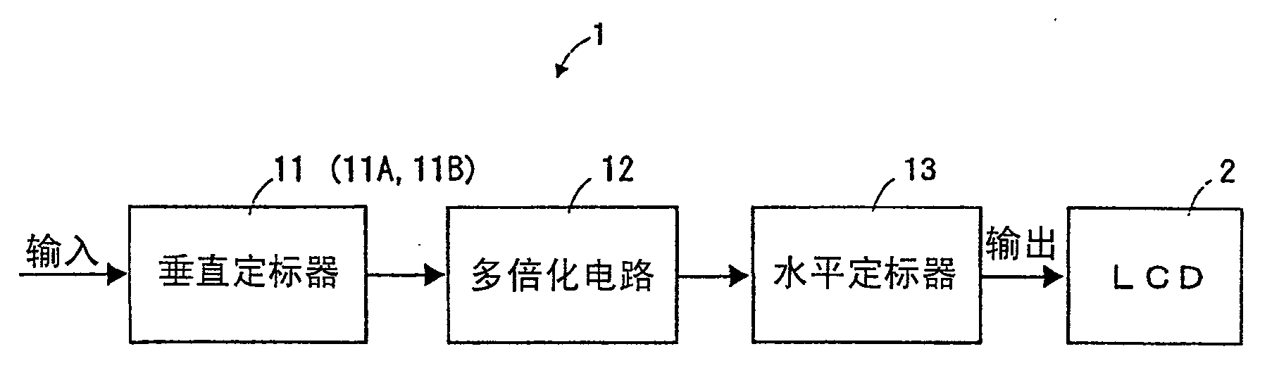
图1是表示图像显示装置的框图。该图像显示装置由图像信号处理电路1和液晶面板(LCD)2构成。图像信号处理电路1由垂直定标器11(11A、11B)、多倍化电路12和水平定标器13构成。输入图像信号是数字化后的图像信号(亮度/色差信号、RGB信号等),并输入到垂直定标器11中。垂直定标器11具有增加输入图像信号的扫描线数的功能。但是,其增加率是1.0左右。例如,在来自垂直定标器11的单位输出行数是M、向垂直定标器11的单位输入行数为N、增加率为α时,满足0<α<2(α=M/N)的条件。即,α为1.0左右。另外,在该实施方式中,α≠1。FIG. 1 is a block diagram showing an image display device. This image display device is composed of an image
作为垂直定标器11,采用图2所示的垂直定标器11A或图4所示的垂直定标器11B。当然,也可不限于此。垂直定标器11A构成为包括一个行存储器11a。图3表示所述行存储器11a的动作时间图。在这里,横轴是时间,纵轴是行存储器11a的地址值。实线表示写入地址,虚线表示读取地址。输入和输出的a、b、c....分别表示一行图像信号。在该例中,表示了M=6、N=5的例子,α=1.2。As the
图3中,若观察行存储器11a的输出,则两次读出一行图像(a),一次读出其他的一行图像(b~e)。结果,将5条扫描线增加为6条。In FIG. 3, when looking at the output of the
图4所示的垂直定标器11B具有可避免两次输出一行图像(a)的电路结构。垂直定标器11B构成为包括第一行存储器11b、第二行存储器11c、第一乘法器11d、第二乘法器11e和加法器11f。第一行存储器11b与前述的行存储器11a同样动作。将第一行存储器11b的输出输入到第一乘法器11d和第二行存储器11c中。第二行存储器11c使输入数据延迟读出系统的一个水平期间后输出。通过第一行存储器11b和第二行存储器11c,构成垂直方向的内插滤波器。The
将由第二行存储器11c延迟后的数据输入到第二乘法器11e中。第一乘法器11d将来自第一行存储器11b的输入数据m倍后输出,第二乘法器11e将来自第二行存储器11c的输入数据n倍后输出。加法器11f输入m倍输出数据和n倍输出数据后输出相加了这些数据的值。The data delayed by the
图5是垂直定标器11B的动作时间图。横轴是时间,纵轴是行存储器的地址值。实线表示写入地址,虚线表示读取地址。从图5可以看出,若为垂直定标器11B,则不会连续两次输出同一图像信号。作为乘法器11d、11e的相乘系数(m)(n),选择例如线性内插两条扫描线信号的常数。例如,可以采用m=0.5、n=0.5。FIG. 5 is an operation time chart of the
为了构成特性更好的内插滤波器,也可在第二行存储器11c的后级进一步从属连接行存储器。In order to configure an interpolation filter with better characteristics, a line memory may be further slave-connected to the subsequent stage of the
图6是表示多倍化电路12的框图。该多倍化电路12构成为包括第三行存储器12a、第四行存储器12b和选择电路12c。第三行存储器12a和第四行存储器12b以输入系统的时钟(对应于第一行存储器11b和第二行存储器11c的写入时钟)以一行为间隔交替进行来自垂直定标器11的图像信号的写入。并且,以该写入时钟的整数倍的时钟(例如1倍、2倍、3倍等)进行读出。FIG. 6 is a block diagram showing the
图7是表示多倍化电路12的处理的时间图。在该例中,以三倍时钟进行读出。在以三倍速度进行读出的情况下,其比值是3/1,为3-1=2,产生了地址超越。因此,并行配置第三行存储器12a和第四行存储器12b。所述选择电路12c选择从第三行存储器12a三次读出的同一图像信号后输出。之后,切换到第四行存储器12b侧,选择从第四行存储器12b三次读出的同一图像信号后输出。并且,再次切换到第三行存储器12a侧,重复同样的切换处理。即,多倍化电路12构成为以三倍的时钟进行读出,同时,不选择因地址超越而读出的图像信号。FIG. 7 is a timing chart showing the processing of the
水平定标器13从多倍化电路12输入图像信号,并将该图像信号的水平点数转换为液晶面板2的水平点数。例如,在液晶面板2是XGA面板的情况下,将输入信号(720点)转换为XGA面板的水平分辨率(1024点)。该转换也可使用一维的内插滤波器。The
如上面所说明的,上述系统的最末级的总输出图像扫描线数M’可以表现为M’=N’×α×K=N’×(M/N)×K。这里,N’是总输入图像扫描数,K是多倍化电路12的倍化数(放大率),具有K=1、2、3、...的值(自然数)。As explained above, the total output image scanning line number M' of the last stage of the above system can be expressed as M'=N'×α×K=N'×(M/N)×K. Here, N' is the total number of input image scans, K is the number of times (magnification) of the
假定将1半帧240行的NTSC信号显示为VGA面板的情况,设α=20/19=1.05263,若K=2,则总输出图像扫描数M’为M’=240×α×K=240×1.0526×2=505行。Assuming that the NTSC signal of 240 lines in one field is displayed as a VGA panel, set α=20/19=1.05263, if K=2, then the total output image scanning number M' is M'=240×α×K=240 ×1.0526×2=505 rows.
由于VGA面板的垂直分辨率是480行,所以剩余的25行(505-480=25)不显示在面板上,为显示了95%的状态。通常,在CRT电视中也相同,但是若100%显示输入图像信号,则在如VTR再现时那样,显示了同步不稳定、不完全基于NTSC(PAL)标准的信号时,存在显示了噪声的情况,通常需要显示100%以下的区域。Since the vertical resolution of the VGA panel is 480 lines, the remaining 25 lines (505−480=25) are not displayed on the panel, which is 95% of the displayed state. Generally, the same is true for CRT TVs, but if 100% of the input video signal is displayed, noise may be displayed when a signal whose synchronization is not stable or not completely based on the NTSC (PAL) standard is displayed as in the case of VTR playback. , usually need to display the area below 100%.
另外,若假定为在XGA面板(垂直分辨率=768)上的显示,α=9/8=1.125,K=3,则为总扫描线数M’=α×3×240=1.125×3×240=810,显示率=768/810=0.948。In addition, if it is assumed to be displayed on an XGA panel (vertical resolution = 768), α = 9/8 = 1.125, K = 3, then the total number of scanning lines M' = α × 3 × 240 = 1.125 × 3 × 240=810, display rate=768/810=0.948.
图8是表示各种图像显示面板的分辨率、各种图像信号的形式、输入图像的有效扫描线数、显示率、面板的显示行数、多倍化电路的放大率K和增加率α的关系的说明图。增加率α可以从约0.66到约1.58的范围中选择。但是,NTSC的扫描线数是525行,PAL的扫描线数是625行。在NTSC的情况下,如(525/2)×(22/21)=275那样,为整数(分子是M,分母是N)。另外,在PAL的情况下,若为(625/2)×(偶数/5或25或125或625),为整数。通过成为整数,电路制作容易。在所述的图8中,在增加率α取接近于0.87719的值的情况下,若分母=5、分子=4,则α=0.8,另外,若分母=25、分子=22,则α=0.88,都可以。另外,若分母=25、分子=24,也可以在α=0.96下将显示率设为0.86。而且,显示率在各公司的显示面板中不恒定,大致是0.9到0.95的范围。Fig. 8 shows the resolution of various image display panels, the form of various image signals, the number of effective scanning lines of the input image, the display rate, the number of display lines of the panel, the amplification factor K and the increase rate α of the multiplexing circuit An illustration of the relationship. The increase rate a can be selected from the range of about 0.66 to about 1.58. However, NTSC has 525 scanning lines, and PAL has 625 scanning lines. In the case of NTSC, it is an integer such as (525/2)×(22/21)=275 (the numerator is M and the denominator is N). Also, in the case of PAL, if it is (625/2)×(even number/5 or 25 or 125 or 625), it is an integer. By being an integer, circuit fabrication is easy. In said Fig. 8, when the increase rate α takes a value close to 0.87719, if denominator=5, numerator=4, then α=0.8, in addition, if denominator=25, numerator=22, then α= 0.88 is fine. In addition, if the denominator=25 and the numerator=24, the display rate may be set to 0.86 at α=0.96. Furthermore, the display ratio is not constant among the display panels of various companies, but generally ranges from 0.9 to 0.95.
如上面所说明的,由于使用增加率α为0<α<2(即,α是1.0左右)的垂直定标器11,所以可以减小画质的劣化,且可以减小电路规模。进一步,通过组合到该垂直定标器11中来使用多倍化电路12,从而可以实现最终需要的垂直尺度处理,且可以极大减小该电路规模。As explained above, since the
另外,在上面说明的例子中,在垂直定标器11的后级上设置了多倍化电路12,但是并不限于此,垂直定标器11和多倍化电路12的配置关系也可相反。另外,在上面的说明中,表示了驱动液晶面板的例子,但是并不限于此。本发明的图像显示装置在用于液晶面板等所谓的保持型显示元件的驱动的情况下尤其实现了图像质量的提高。In addition, in the above-described example, the multiplexing
(第二实施方式)(second embodiment)
下面,根据图9到图15说明本发明的实施方式。Next, an embodiment of the present invention will be described with reference to FIGS. 9 to 15 .
图9是表示了驱动液晶面板115的显示器驱动装置101的框图。所输入的图像信号是数字化后的图像信号(亮度/色差信号、RGB信号等)。将图像信号输入到驱动装置1的垂直定标器111(111A、111B)中。垂直定标器111具有增加输入图像信号的扫描线数的功能。其中,其增加率是1.0左右。例如,在来自垂直定标器111的单位输出行数是M、向垂直定标器111的单位输入行数为N、增加率为α时,满足α=M/N、0<α<2的条件。即,α为1.0左右。另外,在该实施方式中,α≠1。FIG. 9 is a block diagram showing a
作为垂直定标器111采用图10所示的垂直定标器111A或图12所示的垂直定标器111B。当然,也可不限于此。垂直定标器111A构成为包括一个行存储器111a。图11表示所述行存储器111a的动作时间图。在这里,横轴是时间,纵轴是行存储器111a的地址值。实线表示写入地址,虚线表示读取地址。输入和输出的a、b、c....分别表示一行图像信号。在该例中,表示了M=6、N=5的例子,α=1.2。As the
在图11中,若观察行存储器111a的输出,则两次读出一行图像(a),一次读出其他的一行图像(b~e)。结果,将5条扫描线增加为6条。In FIG. 11, when looking at the output of the
图12所示的垂直定标器111B具有可避免两次输出一行图像(a)的电路结构。垂直定标器111B构成为包括第一行存储器111b、第二行存储器111c、第一乘法器111d、第二乘法器111e和加法器111f。第一行存储器111b与前述的行存储器111a同样动作。将第一行存储器111b的输出输入到第一乘法器111d和第二行存储器111c中。第二行存储器111c使输入数据延迟读出系统的一个水平期间后输出。通过第一行存储器111b和第二行存储器111c,构成垂直方向的内插滤波器。The
将由第二行存储器111c延迟后的数据输入到第二乘法器111e中。第一乘法器111d将来自第一行存储器111b的输入数据m倍后输出,第二乘法器111e将来自第二行存储器111c的输入数据n倍后输出。加法器111f输入m倍输出数据和n倍输出数据后输出相加了这些数据的值。The data delayed by the
图13是垂直定标器111B的动作时间图。横轴是时间,纵轴是行存储器的地址值。实线表示写入地址,虚线表示读取地址。从图13可以看出,若为垂直定标器111B,则不会连续两次输出同一图像信号。作为乘法器111d、111e的相乘系数(m)(n),选择例如线性内插两条扫描线信号的常数。例如,可以采用m=0.5、n=0.5。FIG. 13 is an operation time chart of the
为了构成特性更好的内插滤波器,也可在第二行存储器11c的后级进一步从属连接行存储器。In order to configure an interpolation filter with better characteristics, a line memory may be further slave-connected to the subsequent stage of the
水平定标器112将从垂直定标器111输入的图像信号的水平点数转换为液晶面板115的水平点数。例如,在液晶面板115是XGA面板的情况下,将输入信号(720点)转换为XGA面板的水平分辨率(1024点)。该转换也可使用一维的内插滤波器。The
图14是表示液晶模块113的多行同时写入定时控制器(下面,仅称作控制器)114和液晶面板115的电路图。图15是表示所述控制器114的动作的时间图。14 is a circuit diagram showing a multi-line simultaneous writing timing controller (hereinafter, simply referred to as a controller) 114 of a
使用两图来说明多行同时写入的动作。输入信号通常是RGB各8比特的数字信号。首先,说明通常的图像显示方法。在使能信号EN为高(1)时,输入信号依次通过移位寄存器来移位。并且,在一行图像信号的移位结束的时刻,通过从定时生成电路114a输出的锁存脉冲将各数据取入到锁存电路内。这时,若由栅极驱动器行选择脉冲生成电路114b选择的行号为0,则将D/A转换后的图像信号写入到行0中。同样,将行选择依次移位为1、2、3,而在面板上显示图像。在这里,移位寄存器和D/A转换器的个数与面板的水平分辨率一致,在XGA面板的情况下是1024个。另外,垂直行的数目是768行。多行同时写入如图15所示,在D/A转换器输出为图像A时,选择行0和行1,而将图像A写入到行0和行1中。同样,在D/A转换器输出为图像B时,选择行2和3,将图像B写入到行2和行3中。该例子虽然是两行同时写入,但即使是三行同时写入或四行同时写入也为同样的原理。Use two diagrams to illustrate the operation of simultaneously writing multiple rows. The input signal is usually a digital signal of 8 bits each for RGB. First, a general image display method will be described. When the enable signal EN is high (1), the input signals are sequentially shifted through the shift register. Then, each data is taken into the latch circuit by the latch pulse output from the
如上面所说明的,上述系统中最末级的总输出图像扫描线数M’可以表现为M’=N’×α×K=N’×(M/N)×K。这里,N’是总输入图像扫描数,K是控制器114进行的同时写入数,具有K=1、2、3、...的值(自然数)。As explained above, the total output image scanning line number M' of the final stage in the above system can be expressed as M'=N'×α×K=N'×(M/N)×K. Here, N' is the total number of input image scans, K is the number of simultaneous writing performed by the
假定将1半帧240行的NTSC信号显示为VGA面板的情况,设α=20/19=1.05263,若K=2,总输出图像扫描数M’为M’=240×α×K=240×1.0526×2=505行。Assuming that the NTSC signal of 1 field and 240 lines is displayed as a VGA panel, set α=20/19=1.05263, if K=2, the total output image scanning number M' is M'=240×α×K=240× 1.0526×2=505 rows.
由于VGA面板的垂直分辨率是480行,所以剩余的25行(505-480=25)不显示在面板上,为显示了95%的状态。通常,在CRT电视中也相同,但是若100%显示输入图像信号,则如VTR再现时那样,在显示同步不稳定、不完全基于NTSC(PAL)标准的信号时,存在显示了噪声的情况,通常需要显示100%以下的区域。Since the vertical resolution of the VGA panel is 480 lines, the remaining 25 lines (505−480=25) are not displayed on the panel, which is 95% of the displayed state. Usually, the same is true for CRT TVs, but if 100% of the input image signal is displayed, as in VTR reproduction, when displaying a signal with unstable synchronization and not completely based on the NTSC (PAL) standard, noise may be displayed. Typically it is desirable to display the area below 100%.
另外,若假定为在XGA面板(垂直分辨率=768)上的显示,α=9/8=1.125,K=3,则为总扫描线数M’=α×3×240=1.125×3×240=810,显示率=768/810=0.948。In addition, if it is assumed to be displayed on an XGA panel (vertical resolution = 768), α = 9/8 = 1.125, K = 3, then the total number of scanning lines M' = α × 3 × 240 = 1.125 × 3 × 240=810, display rate=768/810=0.948.
实施方式1所示的图8在该实施方式中也可适用。FIG. 8 shown in
如上所说明的,由于使用增加率α为0<α<2(即,α是1.0左右)的垂直定标器111,所以可以减小画质的劣化,且可以减小电路规模。进一步,通过组合到该垂直定标器111中来使用多行同时写入控制器114,从而可以实现最终需要的垂直尺度处理,且可以极大减小该电路规模。As explained above, since the
另外,在上面的说明中,表示了驱动液晶面板的例子,但是并不限于此。本发明的显示器驱动装置在用于液晶面板等所谓的保持型显示元件的驱动的情况下,尤其实现了图像质量的提高。In addition, in the above description, an example of driving a liquid crystal panel was shown, but it is not limited thereto. When the display drive device of the present invention is used to drive a so-called hold type display element such as a liquid crystal panel, image quality can be improved particularly.
Claims (8)
Applications Claiming Priority (3)
| Application Number | Priority Date | Filing Date | Title |
|---|---|---|---|
| JP2004128637A JP2005311886A (en) | 2004-04-23 | 2004-04-23 | Video signal processing circuit and video display apparatus |
| JP2004128637 | 2004-04-23 | ||
| JP2004128638 | 2004-04-23 |
Publications (2)
| Publication Number | Publication Date |
|---|---|
| CN1691127A CN1691127A (en) | 2005-11-02 |
| CN100409682C true CN100409682C (en) | 2008-08-06 |
Family
ID=35346516
Family Applications (1)
| Application Number | Title | Priority Date | Filing Date |
|---|---|---|---|
| CNB2005100669524A Expired - Fee Related CN100409682C (en) | 2004-04-23 | 2005-04-22 | Image signal processing circuit, image display device and display drive device |
Country Status (2)
| Country | Link |
|---|---|
| JP (1) | JP2005311886A (en) |
| CN (1) | CN100409682C (en) |
Citations (6)
| Publication number | Priority date | Publication date | Assignee | Title |
|---|---|---|---|---|
| CN1203492A (en) * | 1997-06-19 | 1998-12-30 | 松下电器产业株式会社 | video signal converter |
| JPH11164266A (en) * | 1997-11-27 | 1999-06-18 | Matsushita Electric Ind Co Ltd | Video signal processing device |
| JPH11259053A (en) * | 1998-03-06 | 1999-09-24 | Victor Co Of Japan Ltd | Liquid crystal display |
| JP2001086470A (en) * | 2000-08-23 | 2001-03-30 | Hitachi Ltd | Video compression / expansion equipment |
| US6219020B1 (en) * | 1995-11-30 | 2001-04-17 | Hitachi, Ltd. | Liquid crystal display control device |
| US6239779B1 (en) * | 1998-03-06 | 2001-05-29 | Victor Company Of Japan, Ltd. | Active matrix type liquid crystal display apparatus used for a video display system |
-
2004
- 2004-04-23 JP JP2004128637A patent/JP2005311886A/en active Pending
-
2005
- 2005-04-22 CN CNB2005100669524A patent/CN100409682C/en not_active Expired - Fee Related
Patent Citations (6)
| Publication number | Priority date | Publication date | Assignee | Title |
|---|---|---|---|---|
| US6219020B1 (en) * | 1995-11-30 | 2001-04-17 | Hitachi, Ltd. | Liquid crystal display control device |
| CN1203492A (en) * | 1997-06-19 | 1998-12-30 | 松下电器产业株式会社 | video signal converter |
| JPH11164266A (en) * | 1997-11-27 | 1999-06-18 | Matsushita Electric Ind Co Ltd | Video signal processing device |
| JPH11259053A (en) * | 1998-03-06 | 1999-09-24 | Victor Co Of Japan Ltd | Liquid crystal display |
| US6239779B1 (en) * | 1998-03-06 | 2001-05-29 | Victor Company Of Japan, Ltd. | Active matrix type liquid crystal display apparatus used for a video display system |
| JP2001086470A (en) * | 2000-08-23 | 2001-03-30 | Hitachi Ltd | Video compression / expansion equipment |
Also Published As
| Publication number | Publication date |
|---|---|
| JP2005311886A (en) | 2005-11-04 |
| CN1691127A (en) | 2005-11-02 |
Similar Documents
| Publication | Publication Date | Title |
|---|---|---|
| JPH09114443A (en) | Video scaling device | |
| US6507346B1 (en) | Image processing method and image display | |
| US7675480B2 (en) | Image display device and image display method | |
| WO1999026229A1 (en) | System and methods for 2-tap/3-tap flicker filtering | |
| US5196934A (en) | Image scaling apparatus for a multimedia system | |
| CN100409682C (en) | Image signal processing circuit, image display device and display drive device | |
| US7209186B2 (en) | Image processing apparatus and image processing method for high speed real-time processing | |
| JP3863887B2 (en) | Display drive device | |
| US6710810B1 (en) | Video signal processing apparatus with resolution enhancing feature | |
| US7408589B2 (en) | Video signal processing circuit, video display, and display driving device | |
| JP2004110046A (en) | Display device for video scaling | |
| JP3473093B2 (en) | Display system | |
| JPH0573005A (en) | Picture display device | |
| TW525144B (en) | Image display device | |
| JP3895946B2 (en) | Display device and control circuit thereof | |
| JPH03236097A (en) | Method and device for image display | |
| JPH0573004A (en) | Picture display device | |
| JP2000148059A (en) | Line number conversion processing circuit and display device equipped with the same | |
| JP2000314869A (en) | Active matrix type liquid crystal display device and display method | |
| JP4608889B2 (en) | Liquid crystal display device | |
| JP2001057654A (en) | High sensitivity imaging device | |
| JP2000305538A (en) | Image enlargement method and image enlargement circuit | |
| JP2000020709A (en) | Video signal processor | |
| JPH0575959A (en) | Image display | |
| JP2007058234A (en) | Display device for video scaling |
Legal Events
| Date | Code | Title | Description |
|---|---|---|---|
| C06 | Publication | ||
| PB01 | Publication | ||
| C10 | Entry into substantive examination | ||
| SE01 | Entry into force of request for substantive examination | ||
| C14 | Grant of patent or utility model | ||
| GR01 | Patent grant | ||
| C17 | Cessation of patent right | ||
| CF01 | Termination of patent right due to non-payment of annual fee |
Granted publication date: 20080806 Termination date: 20100422 |