CN100405342C - Bus type connection system for backplanes - Google Patents
Bus type connection system for backplanes Download PDFInfo
- Publication number
- CN100405342C CN100405342C CNB2004100801788A CN200410080178A CN100405342C CN 100405342 C CN100405342 C CN 100405342C CN B2004100801788 A CNB2004100801788 A CN B2004100801788A CN 200410080178 A CN200410080178 A CN 200410080178A CN 100405342 C CN100405342 C CN 100405342C
- Authority
- CN
- China
- Prior art keywords
- section
- line
- bus
- given
- sections
- Prior art date
- Legal status (The legal status is an assumption and is not a legal conclusion. Google has not performed a legal analysis and makes no representation as to the accuracy of the status listed.)
- Expired - Fee Related
Links
Images


Classifications
-
- G—PHYSICS
- G06—COMPUTING OR CALCULATING; COUNTING
- G06F—ELECTRIC DIGITAL DATA PROCESSING
- G06F13/00—Interconnection of, or transfer of information or other signals between, memories, input/output devices or central processing units
- G06F13/38—Information transfer, e.g. on bus
- G06F13/40—Bus structure
- G06F13/4063—Device-to-bus coupling
- G06F13/409—Mechanical coupling
-
- G—PHYSICS
- G06—COMPUTING OR CALCULATING; COUNTING
- G06F—ELECTRIC DIGITAL DATA PROCESSING
- G06F30/00—Computer-aided design [CAD]
- G06F30/30—Circuit design
-
- G—PHYSICS
- G06—COMPUTING OR CALCULATING; COUNTING
- G06F—ELECTRIC DIGITAL DATA PROCESSING
- G06F30/00—Computer-aided design [CAD]
- G06F30/30—Circuit design
- G06F30/36—Circuit design at the analogue level
- G06F30/367—Design verification, e.g. using simulation, simulation program with integrated circuit emphasis [SPICE], direct methods or relaxation methods
Landscapes
- Engineering & Computer Science (AREA)
- Computer Hardware Design (AREA)
- Theoretical Computer Science (AREA)
- Physics & Mathematics (AREA)
- General Engineering & Computer Science (AREA)
- General Physics & Mathematics (AREA)
- Evolutionary Computation (AREA)
- Geometry (AREA)
- Microelectronics & Electronic Packaging (AREA)
- Dc Digital Transmission (AREA)
- Cable Transmission Systems, Equalization Of Radio And Reduction Of Echo (AREA)
Abstract
本发明涉及一种特别针对电子系统的布线背板的总线连接系统,这里的总线包括不规律分布的连接器。它包括选择段,在每段中连接器之间的间隔是基本相同的,除了一段以外,改变所有线段的结构,使得改变的各段的有效阻抗与未修改的一段的有效阻抗相等。这就产生了从一端到另一端都满足匹配要求的总线,并且可以工作在很高的频率上,仅仅是轻微地减小了其传播常数。
The present invention relates to a bus connection system especially for a wiring backplane of an electronic system, where the bus includes irregularly distributed connectors. It consists of selecting sections in which the spacing between connectors is substantially the same, and changing the configuration of all but one section so that the effective impedance of the changed sections is equal to the effective impedance of the unmodified section. This produces a bus that is matched from end to end and can operate at very high frequencies with only a slight reduction in its propagation constant.
Description
技术领域 technical field
本发明涉及总线类型连接系统,即涉及包括一对或者多对两线(two wire)线路的连接系统,在该系统中用于连接电子设备的连接器可以位于线路的任意位置。The present invention relates to a connection system of the bus type, that is to say a connection system comprising one or more pairs of two wire lines in which the connectors for connecting electronic devices can be located at any position on the line.
在编码系统的帮助下,在总线上收发线路上传播的信息,一般地,该编码系统是时间编码系统,它决定了当前传送的信息所相关的设备。总线通常包括一组线路,用于平行地传输信息。这种系统广泛地应用于个人电脑(PC)中,用来连接扩展卡。它也广泛地应用在专用的电子设备中,用于背板的布线,其中所述背板插有组成需要的硬件的电路卡。The information propagated on the line is sent and received on the bus with the help of a coding system, generally a time coding system, which determines the device to which the currently transmitted information is related. A bus usually consists of a set of wires used to transfer information in parallel. This system is widely used in personal computers (PCs) to connect expansion cards. It is also widely used in dedicated electronic equipment for the wiring of the backplane into which the circuit cards making up the required hardware are plugged.
背景技术 Background technique
连接器通常以相等的间隔固定在背板上,它们通过电导线相连,从一个连接器到下一个连接器的导线的长度都是相同的。这样的组合形成了传输线或者多重传偷线,这些传输线具有固定特征阻抗,可以以很高的频率传偷信号,尤其是数字信号,而信号的畸变很小。The connectors are usually fixed on the backplane at equal intervals, and they are connected by electrical wires, and the wires are all the same length from one connector to the next. Such combinations form transmission lines or multiple transmission lines, which have a fixed characteristic impedance and can transmit signals at high frequencies, especially digital signals, with little signal distortion.
在某些特定的情况下,连接器之间距离不可能保持为相等,沿着线路的特征阻抗更改为是连接器之间距离的函数。这引起沿着线路的传输时间的变化和区域化反射。这些现象导致传输信号的畸变,限制了信号可以被传输的频率。In certain cases where it is not possible to keep the distance between the connectors equal, the characteristic impedance along the line changes as a function of the distance between the connectors. This causes variations in transit time and localized reflections along the line. These phenomena cause distortions in the transmitted signal, limiting the frequencies at which the signal can be transmitted.
发明内容 Contents of the invention
为了克服这些限制,本发明提出了一种总线连接系统,包括传输线,沿着传输线有用来容纳电子线路卡的连接器,传输线包括至少两段,每一段都包括一组按照常数等间隔(d1,d2)设置的连接器,不同段的间隔都是不同的,而且所述电子线路卡改变了所连接的段的阻抗,产生了有效阻抗。相对于其他段的传输线,改变一段传输线自身的结构,使得该段的有效阻抗与其他段的有效阻抗一致。To overcome these limitations, the present invention proposes a bus connection system comprising a transmission line along which there are connectors for receiving electronic circuit cards, the transmission line comprising at least two segments, each segment comprising a set of , d 2 ) For the connectors provided, the intervals of different segments are different, and the electronic circuit card changes the impedance of the connected segments, resulting in an effective impedance. Compared with the transmission lines of other sections, the structure of a transmission line itself is changed so that the effective impedance of this section is consistent with the effective impedance of other sections.
本解决方案的优点在于除了需要正确的传输线的参数以外,并不涉及任何额外的制造成本。The advantage of this solution is that it does not involve any additional manufacturing costs beyond the need for correct transmission line parameters.
根据另一特征,所述系统用于背板。According to another feature, the system is used for backplanes.
根据另一特征,所述至少两段分别具有在所述段的相应连接器之间不同的间隔,除了给定的一段以外,其他各段传输线的结构都相对于所述给定的一段修改,以保证它们的有效阻抗与所述给定的一段相同。According to another feature, said at least two segments each have a different spacing between the respective connectors of said segments, except for a given segment, the configuration of which is modified relative to said given segment, To ensure that their effective impedance is the same as the given section.
根据另一特征,所述给定的一段的有效阻抗是最低的。According to another feature, said given segment has the lowest effective impedance.
根据另一特征,所述给定的一段的连接器间隔(d2)是最短的。According to another feature, said given segment has the shortest connector separation (d 2 ).
根据另一特征,每段线都是给定厚度的导体线段,通过改变线的宽度来改变线的结构。According to another feature, each line segment is a conductor line segment of a given thickness, the structure of the line being varied by varying the width of the line.
根据另一特征,该系统包括一组传输线,所有传输线都是通过相同的方式来修改的。According to another feature, the system comprises a set of transmission lines, all of which are modified in the same way.
附图说明 Description of drawings
通过阅读后续描述,本发明的其他特征和优点将会变得很清晰,后续描述将参照附图进行,其中:Other features and advantages of the present invention will become apparent on reading the ensuing description, which will be made with reference to the accompanying drawings, in which:
图1示出了包括两个不匹配部分的总线;Figure 1 shows a bus comprising two mismatched parts;
图2示出了根据本发明修改过的图1所示的总线;Figure 2 shows the bus shown in Figure 1 modified according to the present invention;
图3是图1所示的总线上的信号图,以及Figure 3 is a signal diagram on the bus shown in Figure 1, and
图4是图2所示的总线上的信号图。FIG. 4 is a signal diagram on the bus shown in FIG. 2 .
具体实施方式 Detailed ways
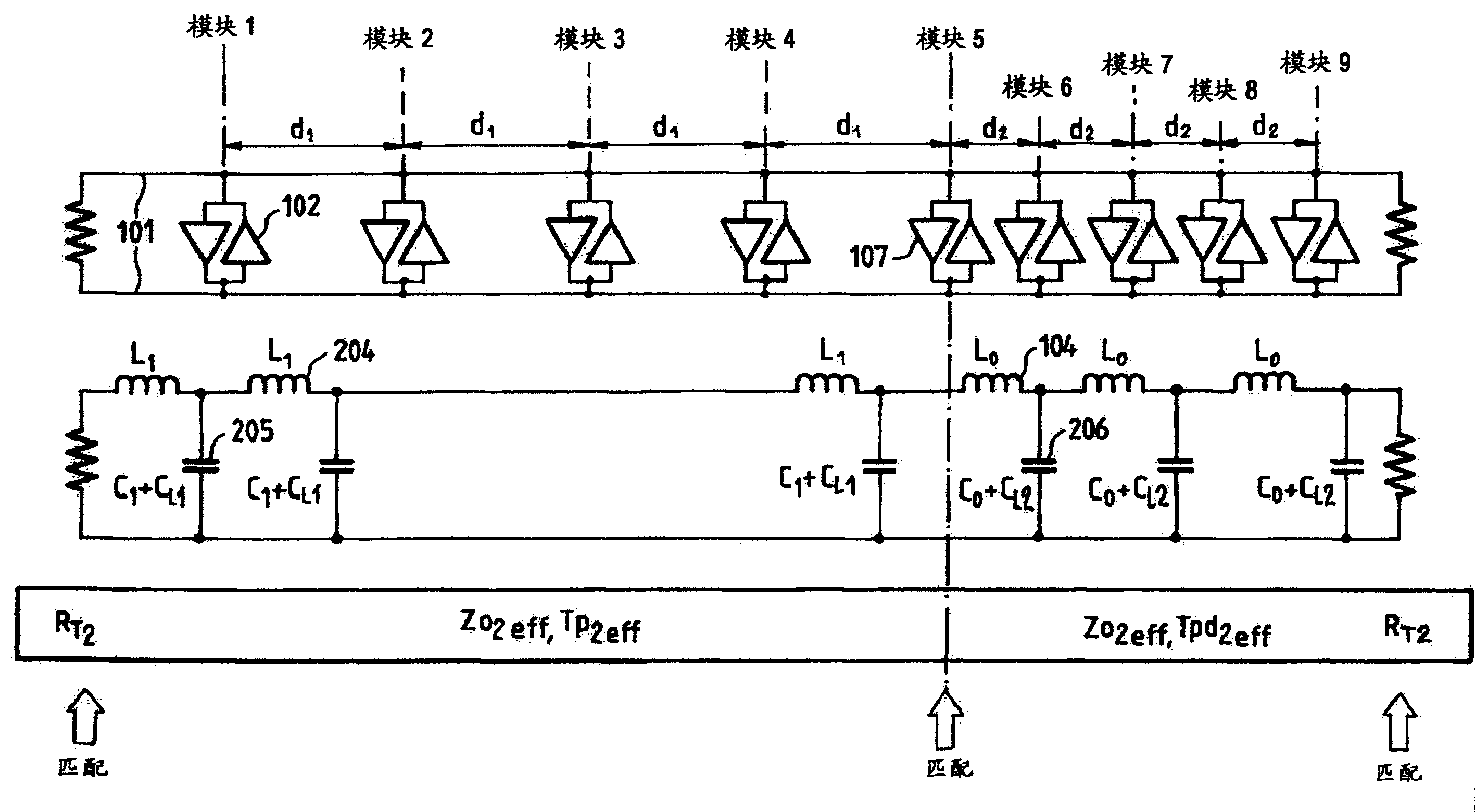
图1既略地示出了本发明的一个特定实施方式,它对应于总长度为D1+D2=75厘米(cm)的一背板总线。为了便于解释,图中只示出了一条与信号相关联的线路,虽然应当理解,总线通常包括很多线路,在那种情况下,本发明以相同方式应用于总线的每一条线路上。FIG. 1 schematically shows a particular embodiment of the invention, which corresponds to a backplane bus with a total length D1+D2=75 centimeters (cm). For ease of explanation, only one line is shown associated with a signal, although it should be understood that a bus will generally include many lines, in which case the invention applies in the same manner to each line of the bus.
为了在40MHz的频率下使用上述总线,需要采用一定的技术,例如使用导线的微带线(strip-line)技术,因此采取了带有分布式常数的传输线的形式,它的特征阻抗由下列参数决定,例如:L0=4.73纳秒/厘米(nH/cm);C0=1.06皮法/厘米(pF/cm);Z0=67欧姆(Ω);Tpd=70.7皮秒/厘米(ps/cm)In order to use the above-mentioned bus at a frequency of 40MHz, certain technologies need to be adopted, such as the strip-line technology using wires, so the form of a transmission line with a distributed constant is adopted, and its characteristic impedance is determined by the following parameters Determine, for example: L0 = 4.73 nanoseconds/centimeter (nH/cm); C0 = 1.06 picofarads/centimeter (pF/cm); Z0 = 67 ohms (Ω); Tpd = 70.7 picoseconds/centimeter (ps/cm)
图中上面部分的物理表现示出了一组输入/输出缓存放大器102,对应于通过连结器(图中没有示出)连接到线101上的线路卡。此线路的两端通过匹配电阻103完成回环。The physical representation of the upper part of the figure shows a set of input/
因为此实施例的特殊原因,第一4个输入/输出放大器按照固定的间隔d1在长度为D1的第一段(segment)中排列,最后的5个放大器按照固定的d2在长度为D2的第二段中排列。在当前的这个例子中,d1=10cm,D1=50cm,d2=5cm and D2=25cm。Because of the particularity of this embodiment, the first 4 input/output amplifiers are arranged in a first segment of length D1 at a fixed interval d1 , and the last 5 amplifiers are arranged at a fixed distance d2 in a segment of length D1 Arranged in the second paragraph of D 2 . In the present example, d 1 =10 cm, D 1 =50 cm, d 2 =5 cm and D 2 =25 cm.
每一个放大器从其放置的位置上连接到该线路,这个例子中的额外电容CL等于12pF。Each amplifier is connected to this line from where it is placed, with an additional capacitance CL equal to 12pF in this example.
在图1中的中间部分所示的等效电路中,传输线的行为相当于带有分布常数和一系列感抗的线路,由电感104和并联电容来表示。在整个线路长度上的感抗等于L0。总线的基本电容由放大器的电容而改变,在D1长度上的容抗由电容105来表示,其容抗值等于C0+CL1;在D2长度上的容抗由电容106来表示,其容抗值等于C0+CL2。CL1和CL2的值通过将常数CL除以相应的长度而得到,所以CL1=CL/d1并且CL2=CL/d2。In the equivalent circuit shown in the middle part of Fig. 1, the transmission line behaves as a line with a distributed constant and a series of inductive reactances, represented by an
结果,有效阻抗沿着总线并不始终相等。它在直到第二系列模块的第一个模块107为止的D1长度上等于Zo1eff,在直到线路的端点的D2长度上等于Zo2eff。上述的取值由下列公式给出:As a result, the effective impedance is not always equal along the bus. It is equal to Zo 1eff over the length D 1 up to the
有效的传播时延会受到相同方式的影响,因此:The effective propagation delay is affected in the same way, so:
结果,由图1中下部的符号所表示,总线的阻抗在模块5的位置即对应于D1长度和D2长度的连接处,具有不连续性。然而,两端可以通过终止对应这些位置的特征阻抗的匹配电阻和
本发明提出更改长度D1的总线的传输线结构,由此在这段线路上允许输入/输出放大器102带来的效果,在此段线路上的等效特征阻抗等于长度D2的特征阻抗。在这种情况下,如图2所示(图2与图1使用相同的图例),带有放大器的总线实现了端到端的匹配。出于技术上的考虑,最好降低最大的阻抗,而不要增加最小的阻抗,例如,那些间隔最短的段。The present invention proposes to modify the transmission line structure of the bus of length D1 , thereby allowing the effect of the input/
实现总线的线段结构可以通过调整其几何形状来更改,通常都是改变构成总线的导线的几何参数。通常每段导线的厚度和位置都是固定的,因此只能通过改变线的宽度来改改变其结构。The line segment structure that realizes the bus can be changed by adjusting its geometry, usually by changing the geometric parameters of the wires that make up the bus. Usually the thickness and position of each segment of wire are fixed, so its structure can only be changed by changing the width of the wire.
考虑到物理可能性,通常必须要改变线段D1上的分布感抗204,使其采用其他的值。例如,等于L1,并同时改变分布电容,例如使其容抗值等于C1。总线本身的特征阻抗,例如不考虑放大器102效果的阻抗,等于Z1。此时,Considering the physical possibility, it is usually necessary to change the distributed
因此,可能必须改变两个参数Z1和C1,但是这两个参数不是互相独立的,Z1是根据C1而变化的。根据实践得知,可以使用迭代的方法,例如首先为C1设置合适的初始值,然后使用此初始值来计算Z1的第一个值。Z1的第一个值用来设置总线的参数,例如使用现成的HP_ADS仿真器。如果按照这种方法得到的参数不合适,可以向物理上合适的方向上修改,从而产生Z1和C1的第二个值。计算出相应的阻抗Zo1eff,这个值肯定与Zo2eff不同。根据差别的方向,这个过程可以不断重复,直到收敛到Zo1eff=Zo2eff。得出的等效电容205和206分别是C1+CL1和C0+CL2。Therefore, two parameters Z1 and C1 may have to be varied, but these two parameters are not independent of each other, Z1 is varied according to C1 . It is known from practice that an iterative method can be used, for example, first setting an appropriate initial value for C 1 , and then using this initial value to calculate the first value of Z 1 . The first value of Z 1 is used to set the parameters of the bus, such as using the ready-made HP_ADS emulator. If the parameters obtained in this way are not suitable, they can be modified in a physically suitable direction, resulting in a second value of Z 1 and C 1 . Calculate the corresponding impedance Zo 1eff , which must be different from Zo 2eff . Depending on the direction of the difference, this process can be repeated until it converges to Zo 1eff =Zo 2eff . The resulting
我们已经解释了在两种间隔的情况下的处理方法,这种处理方法同样可以推广到具有多种间隔的情况。We have explained the treatment in the case of two intervals, which can be generalized to the case of multiple intervals as well.
为此,第一步是决定最小的有效阻抗,例如,每一个线段上输入/输出之间都有相同的间隔,通过计算所有部分的阻抗,得到最短间隔的等效阻抗。For this, the first step is to determine the minimum effective impedance, for example, the same interval between input/output on each line segment, by calculating the impedance of all parts, the equivalent impedance of the shortest interval is obtained.
上述的方法可以应用到每一个部分,通过前缀x来识别,得到下面的公式:The above method can be applied to each part, identified by the prefix x, resulting in the following formula:
总线终端的匹配电阻可以使用已知的方法来计算。在图2描述的例子中,因为仅有第一部分的阻抗发生了改变,所以仅有输入电阻203改变了。The matching resistance of the bus termination can be calculated using known methods. In the example depicted in FIG. 2, only the input resistance 203 changes because only the impedance of the first part changes.
最后一步是验证总线对于数字信号工作正常,最好使用上面提到的仿真器。如果得到的电路行为不是很好,重复进行上述的操作来得到另一对C1和L1。The final step is to verify that the bus is working properly for digital signals, preferably using an emulator as mentioned above. If the resulting circuit behavior is not very good, repeat the above operation to obtain another pair of C 1 and L 1 .
图3示出了在图1中总线没有正确匹配的例子中,一个矩形波输入信号Ve和在第5个模块和总线输出端的信号Vs1、Vs2。图4示出了在图2中总线正确匹配的例子中相同的信号。图中的单位是电压伏特和纳秒。可以发现性能的改进是非常显著的。Figure 3 shows a rectangular wave input signal V e and the signals V s1 , V s2 at the output of the fifth module and the bus in the example in Figure 1 where the bus is not properly matched. FIG. 4 shows the same signals in the example in FIG. 2 where the bus is correctly matched. The units in the figure are voltage volts and nanoseconds. It can be found that the performance improvement is very significant.
然而,这些改进是通过损害在总线上的整体传输时间得到的,因为总线上各个线段的传播速度都被降低到与最低的那一段相同。However, these improvements come at the expense of the overall transfer time on the bus, since each segment of the bus is slowed down to the same speed as the lowest segment.
上述描述针对以下情形,即每一段中连接器之间的距离是常数,并且其长度是精确的d1和d2。在现实中这种理想的状况是不可能遇到的,但是如果这些间隔基本上是常数,例如它们保持在一个平均值的周围,本发明仍然可以应用。这个平均值就表明了每段的特征。The above description is for the case where the distance between the connectors in each segment is constant and its length is exactly d 1 and d 2 . This ideal situation is unlikely to be encountered in reality, but the invention is still applicable if the intervals are substantially constant, eg they remain around a mean value. This average indicates the characteristics of each segment.
Claims (7)
Applications Claiming Priority (2)
| Application Number | Priority Date | Filing Date | Title |
|---|---|---|---|
| FR0311281A FR2860316B1 (en) | 2003-09-26 | 2003-09-26 | BUS TYPE CONNECTION SYSTEM, IN PARTICULAR FOR BASKET BASKET |
| FR0311281 | 2003-09-26 |
Publications (2)
| Publication Number | Publication Date |
|---|---|
| CN1601503A CN1601503A (en) | 2005-03-30 |
| CN100405342C true CN100405342C (en) | 2008-07-23 |
Family
ID=34178958
Family Applications (1)
| Application Number | Title | Priority Date | Filing Date |
|---|---|---|---|
| CNB2004100801788A Expired - Fee Related CN100405342C (en) | 2003-09-26 | 2004-09-24 | Bus type connection system for backplanes |
Country Status (4)
| Country | Link |
|---|---|
| US (1) | US7161377B2 (en) |
| EP (1) | EP1519285A1 (en) |
| CN (1) | CN100405342C (en) |
| FR (1) | FR2860316B1 (en) |
Families Citing this family (1)
| Publication number | Priority date | Publication date | Assignee | Title |
|---|---|---|---|---|
| WO2019075224A1 (en) * | 2017-10-11 | 2019-04-18 | Nucleus Scientific, Inc. | Modular bus systems for electric vehicles |
Citations (4)
| Publication number | Priority date | Publication date | Assignee | Title |
|---|---|---|---|---|
| US4858231A (en) * | 1988-05-26 | 1989-08-15 | Northern Telecom Limited | Bus interface loading assembly |
| EP0665647A1 (en) * | 1993-12-29 | 1995-08-02 | International Business Machines Corporation | Pulse signal distribution circuit |
| US6484293B1 (en) * | 2000-07-14 | 2002-11-19 | Sun Microsystems, Inc. | Method for determining optimal configuration for multinode bus |
| US6552564B1 (en) * | 1999-08-30 | 2003-04-22 | Micron Technology, Inc. | Technique to reduce reflections and ringing on CMOS interconnections |
Family Cites Families (8)
| Publication number | Priority date | Publication date | Assignee | Title |
|---|---|---|---|---|
| US4475191A (en) * | 1982-12-10 | 1984-10-02 | At&T Bell Laboratories | Distributed time division multiplexing bus |
| US5146192A (en) * | 1990-07-06 | 1992-09-08 | Hitachi Medical Corporation | Delay circuit of ultrasonic diagnostic apparatus using delay line comprising variable capacitance diode and inductor |
| KR0133217B1 (en) * | 1994-12-20 | 1998-04-21 | 구자홍 | Transmission and reception matching method of wireless communication device and device therefor |
| US6208225B1 (en) * | 1999-02-25 | 2001-03-27 | Formfactor, Inc. | Filter structures for integrated circuit interfaces |
| US6466008B1 (en) * | 2000-10-06 | 2002-10-15 | Hewlett-Packard Company | Method for matching the lengths of signal traces |
| WO2002039582A2 (en) * | 2000-11-09 | 2002-05-16 | Broadcom Corporation | A constant impedance filter |
| JP4111377B2 (en) * | 2002-06-03 | 2008-07-02 | Kddi株式会社 | Impedance matching device and noise reduction filter mounted with the same |
| US6998870B1 (en) * | 2002-07-31 | 2006-02-14 | Advanced Micro Devices, Inc. | Method and apparatus for impedance matching in systems configured for multiple processors |
-
2003
- 2003-09-26 FR FR0311281A patent/FR2860316B1/en not_active Expired - Fee Related
-
2004
- 2004-09-01 EP EP04292144A patent/EP1519285A1/en not_active Withdrawn
- 2004-09-24 US US10/948,152 patent/US7161377B2/en not_active Expired - Fee Related
- 2004-09-24 CN CNB2004100801788A patent/CN100405342C/en not_active Expired - Fee Related
Patent Citations (4)
| Publication number | Priority date | Publication date | Assignee | Title |
|---|---|---|---|---|
| US4858231A (en) * | 1988-05-26 | 1989-08-15 | Northern Telecom Limited | Bus interface loading assembly |
| EP0665647A1 (en) * | 1993-12-29 | 1995-08-02 | International Business Machines Corporation | Pulse signal distribution circuit |
| US6552564B1 (en) * | 1999-08-30 | 2003-04-22 | Micron Technology, Inc. | Technique to reduce reflections and ringing on CMOS interconnections |
| US6484293B1 (en) * | 2000-07-14 | 2002-11-19 | Sun Microsystems, Inc. | Method for determining optimal configuration for multinode bus |
Also Published As
| Publication number | Publication date |
|---|---|
| FR2860316B1 (en) | 2006-05-19 |
| US7161377B2 (en) | 2007-01-09 |
| US20050068061A1 (en) | 2005-03-31 |
| CN1601503A (en) | 2005-03-30 |
| EP1519285A1 (en) | 2005-03-30 |
| FR2860316A1 (en) | 2005-04-01 |
Similar Documents
| Publication | Publication Date | Title |
|---|---|---|
| KR100750038B1 (en) | Compact electromagnetic coupler for use with digital transmission systems | |
| JP4545391B2 (en) | Semiconductor memory device having data bus structure for reducing high frequency noise | |
| US6081430A (en) | High-speed backplane | |
| US7961003B2 (en) | Multi-drop bus system | |
| EP0923277B1 (en) | Printed circuit board | |
| US5650757A (en) | Impedance stepping for increasing the operating speed of computer backplane busses | |
| CN100405342C (en) | Bus type connection system for backplanes | |
| CN106507583A (en) | A signal transmission line, method and system | |
| KR100399594B1 (en) | system board and impedance control method thereof | |
| JP4451614B2 (en) | Data bus having individually matched line impedance and method for matching line impedance | |
| JP6157095B2 (en) | Bus system | |
| JP2020123774A (en) | Communication system | |
| KR20040012366A (en) | Memory system | |
| US6366972B1 (en) | Multi-user communication bus with a resistive star configuration termination | |
| JP4522056B2 (en) | 4-drop bus for consistent response | |
| US20040225807A1 (en) | Method and assembly having a matched filter connector | |
| CN100478934C (en) | High speed memory module utilizing inline capacitors | |
| CN102957411A (en) | Multi-load topological hardware framework | |
| US6756862B2 (en) | Six-drop bus with matched response | |
| JPH05341892A (en) | Information processing equipment | |
| CN115413117A (en) | Differential signal high-speed inter-board interconnection device used in electronic system equipment | |
| US20070170971A1 (en) | Signal transmitting circuit | |
| JP2004272547A (en) | Backboard pattern wiring | |
| CN101001081A (en) | Differential terminal to termial connection circuit | |
| CN1973276A (en) | High speed memory modules |
Legal Events
| Date | Code | Title | Description |
|---|---|---|---|
| C06 | Publication | ||
| PB01 | Publication | ||
| C10 | Entry into substantive examination | ||
| SE01 | Entry into force of request for substantive examination | ||
| C14 | Grant of patent or utility model | ||
| GR01 | Patent grant | ||
| C19 | Lapse of patent right due to non-payment of the annual fee | ||
| CF01 | Termination of patent right due to non-payment of annual fee |