CN100383954C - Memory element and array, method for manufacturing contact structure, and manufactured device and element - Google Patents
Memory element and array, method for manufacturing contact structure, and manufactured device and element Download PDFInfo
- Publication number
- CN100383954C CN100383954C CNB2005101155674A CN200510115567A CN100383954C CN 100383954 C CN100383954 C CN 100383954C CN B2005101155674 A CNB2005101155674 A CN B2005101155674A CN 200510115567 A CN200510115567 A CN 200510115567A CN 100383954 C CN100383954 C CN 100383954C
- Authority
- CN
- China
- Prior art keywords
- contact structure
- memory
- shaped contact
- shaped
- conductive member
- Prior art date
- Legal status (The legal status is an assumption and is not a legal conclusion. Google has not performed a legal analysis and makes no representation as to the accuracy of the status listed.)
- Expired - Lifetime
Links
Images


Classifications
-
- H—ELECTRICITY
- H10—SEMICONDUCTOR DEVICES; ELECTRIC SOLID-STATE DEVICES NOT OTHERWISE PROVIDED FOR
- H10B—ELECTRONIC MEMORY DEVICES
- H10B63/00—Resistance change memory devices, e.g. resistive RAM [ReRAM] devices
- H10B63/20—Resistance change memory devices, e.g. resistive RAM [ReRAM] devices comprising selection components having two electrodes, e.g. diodes
-
- H—ELECTRICITY
- H10—SEMICONDUCTOR DEVICES; ELECTRIC SOLID-STATE DEVICES NOT OTHERWISE PROVIDED FOR
- H10B—ELECTRONIC MEMORY DEVICES
- H10B63/00—Resistance change memory devices, e.g. resistive RAM [ReRAM] devices
- H10B63/30—Resistance change memory devices, e.g. resistive RAM [ReRAM] devices comprising selection components having three or more electrodes, e.g. transistors
-
- H—ELECTRICITY
- H10—SEMICONDUCTOR DEVICES; ELECTRIC SOLID-STATE DEVICES NOT OTHERWISE PROVIDED FOR
- H10N—ELECTRIC SOLID-STATE DEVICES NOT OTHERWISE PROVIDED FOR
- H10N70/00—Solid-state devices having no potential barriers, and specially adapted for rectifying, amplifying, oscillating or switching
- H10N70/011—Manufacture or treatment of multistable switching devices
-
- H—ELECTRICITY
- H10—SEMICONDUCTOR DEVICES; ELECTRIC SOLID-STATE DEVICES NOT OTHERWISE PROVIDED FOR
- H10N—ELECTRIC SOLID-STATE DEVICES NOT OTHERWISE PROVIDED FOR
- H10N70/00—Solid-state devices having no potential barriers, and specially adapted for rectifying, amplifying, oscillating or switching
- H10N70/20—Multistable switching devices, e.g. memristors
- H10N70/231—Multistable switching devices, e.g. memristors based on solid-state phase change, e.g. between amorphous and crystalline phases, Ovshinsky effect
-
- H—ELECTRICITY
- H10—SEMICONDUCTOR DEVICES; ELECTRIC SOLID-STATE DEVICES NOT OTHERWISE PROVIDED FOR
- H10N—ELECTRIC SOLID-STATE DEVICES NOT OTHERWISE PROVIDED FOR
- H10N70/00—Solid-state devices having no potential barriers, and specially adapted for rectifying, amplifying, oscillating or switching
- H10N70/801—Constructional details of multistable switching devices
- H10N70/821—Device geometry
- H10N70/826—Device geometry adapted for essentially vertical current flow, e.g. sandwich or pillar type devices
-
- H—ELECTRICITY
- H10—SEMICONDUCTOR DEVICES; ELECTRIC SOLID-STATE DEVICES NOT OTHERWISE PROVIDED FOR
- H10N—ELECTRIC SOLID-STATE DEVICES NOT OTHERWISE PROVIDED FOR
- H10N70/00—Solid-state devices having no potential barriers, and specially adapted for rectifying, amplifying, oscillating or switching
- H10N70/801—Constructional details of multistable switching devices
- H10N70/841—Electrodes
- H10N70/8418—Electrodes adapted for focusing electric field or current, e.g. tip-shaped
-
- H—ELECTRICITY
- H10—SEMICONDUCTOR DEVICES; ELECTRIC SOLID-STATE DEVICES NOT OTHERWISE PROVIDED FOR
- H10N—ELECTRIC SOLID-STATE DEVICES NOT OTHERWISE PROVIDED FOR
- H10N70/00—Solid-state devices having no potential barriers, and specially adapted for rectifying, amplifying, oscillating or switching
- H10N70/801—Constructional details of multistable switching devices
- H10N70/881—Switching materials
- H10N70/882—Compounds of sulfur, selenium or tellurium, e.g. chalcogenides
- H10N70/8828—Tellurides, e.g. GeSbTe
-
- H10W20/063—
Landscapes
- Engineering & Computer Science (AREA)
- Manufacturing & Machinery (AREA)
- Semiconductor Memories (AREA)
Abstract
Description
技术领域 technical field
本发明涉及半导体元件及其制造方法,且特别涉及用于相变型存储元件的接触结构的制造方法、含此种接触结构的存储器元件及存储单元阵列,以及使用该方法所制造的电子装置与半导体元件。The present invention relates to a semiconductor element and a manufacturing method thereof, and in particular to a manufacturing method for a contact structure of a phase-change memory element, a memory element and a memory cell array containing such a contact structure, and electronic devices and devices manufactured using the method semiconductor components.
背景技术 Background technique
固态存储器元件广泛使用于电子学领域中。典型的存储器包括动态随机存取存储器(DRAM)、静态随机存取存储器(SRAM)、只读存储器(ROM)、可擦可编程只读存储器(EPROM)、电可擦可编程只读存储器(E2PROM)及闪存等,其可区分为易失与非易失存储器两大类。E2PROM等非易失存储器的主要构件基本上为具浮置栅的场效应晶体管,而在程序化任一存储位时,电荷存入场效应晶体管的浮置栅中。然而,此类存储器的可再程序化次数有限,且其程序化速度也可能相当低。另外,虽然SRAM、ROM、EPROM、E2PROM及闪存的存储单元不须进行数据更新(refreshing),但与易失性的DRAM元件相比之下,其尚有储存密度较低,尺寸较大及制造成本较高等缺点。Solid state memory elements are widely used in the field of electronics. Typical memories include dynamic random access memory (DRAM), static random access memory (SRAM), read only memory (ROM), erasable programmable read only memory (EPROM), electrically erasable programmable read only memory (EEPROM) 2 PROM) and flash memory, which can be divided into two categories: volatile and non-volatile memory. The main components of non-volatile memory such as E 2 PROM are basically field effect transistors with floating gates, and when programming any memory bit, charges are stored in the floating gates of the field effect transistors. However, this type of memory can be reprogrammed a limited number of times, and its programming speed can also be rather slow. In addition, although the storage units of SRAM, ROM, EPROM, E 2 PROM and flash memory do not need to refresh data, compared with volatile DRAM components, they still have lower storage density and larger size. and higher manufacturing costs.
公知技术已有由相变型存储单元所构成,可随机存取且具非易失性的存储装置,其特性与许多商业化存储装置中所使用的电荷储存型存储单元不同。本文中“存储材料”一词指可因外界刺激而产生结构相变的材料,例如是硫族(chalcogenide)材料等相变材料。众所周知,电子存储器领域可用的相变型存储材料,例如是可在通常为非晶相的第一结构状态与通常为结晶相的第二结构状态之间以电切换者。相变型存储材料也可能可在完全非晶态到完全结晶态间多个不同的局部有序状态之间切换,只要这些状态可以检测区别即可。这些材料亦具有真正的非易失性,因其一旦被设定成结晶相、半结晶相、非晶相或半非晶相,即具有固定的电阻值。此电阻值可一直维持到其被重设之前,而可代表此材料的物理状态,如结晶相或非晶相。In the prior art, there are random-access and non-volatile memory devices composed of phase-change memory cells, which are different from the charge-storage memory cells used in many commercial memory devices. The term "storage material" herein refers to a material that can undergo a structural phase change due to external stimuli, such as a phase change material such as a chalcogenide material. As is well known, phase-change memory materials available in the field of electronic memory are, for example, those that can be electrically switched between a first structural state that is usually an amorphous phase and a second structural state that is usually a crystalline phase. Phase-change memory materials may also be switchable between multiple different states of local order from fully amorphous to fully crystalline, as long as these states can be differentiated detectably. These materials are also truly non-volatile because they have a fixed resistance value once set into a crystalline, semi-crystalline, amorphous or semi-amorphous phase. This resistance value is maintained until it is reset, and can represent the physical state of the material, such as crystalline or amorphous phase.
由于相变型存储材料有很大的电阻变化范围,故理论上可容许多位的二进制数据储存在单一存储单元中。达此目的的可能做法,即是以模拟方式为二进制元信息编码,将一段被编码的二进制数据的多个位对应至多个不同电阻值中的一个,再据以程序化单一存储单元。如此,相变型存储器的操作即可如同传统的二进制存储器,或如同进位数大于2的存储器。Since the phase-change memory material has a large resistance variation range, it is theoretically possible to store multi-bit binary data in a single memory cell. A possible way to achieve this goal is to encode binary meta-information in an analog manner, and map multiple bits of a piece of encoded binary data to one of multiple different resistance values, and then program a single memory cell accordingly. In this way, the operation of the phase-change memory can be like a traditional binary memory, or a memory with a carry number greater than 2.
适合用作相变存储材料的典型材料包括各种含硫族材料。用作相变存储材料的典型含硫族材料例如可含有碲(Te)、硒(Se)、锗(Ge)、锑(Sb)、铋(Bi)、铅(Pb)、锡(Sn)、砷(As)、硫(S)、硅(Si)及磷(P)中的至少一种与/或氧。此种非易失存储器元件例如可使用一整块的硫族材料来制作,且至少在理论上,制得的存储器结构可仅以很小的芯片面积来储存一位的数据,故可得本质上高密度的存储芯片。Typical materials suitable for use as phase change memory materials include various chalcogenide-containing materials. Typical chalcogenide-containing materials used as phase-change memory materials may contain, for example, tellurium (Te), selenium (Se), germanium (Ge), antimony (Sb), bismuth (Bi), lead (Pb), tin (Sn), At least one of arsenic (As), sulfur (S), silicon (Si), and phosphorus (P), and/or oxygen. This kind of non-volatile memory element can be fabricated using a monolithic chalcogenide material, and at least in theory, the fabricated memory structure can store one bit of data with only a small chip area, so the essential on high-density memory chips.
然而,相变型存储器元件等固态存储元件(solid-state memory device)的共同特性即是其高耗电量,特别是在(重)设定存储器元件时。即使在构件尺寸不断缩小的情形下,耗电量仍是不可忽视的重要课题,特别是在以电池等电力单元(power cell)供电的可携式装置中。因此,如何降低存储器元件的耗电量一直是须优先处理的问题。However, a common characteristic of solid-state memory devices such as phase-change memory devices is their high power consumption, especially when (re)setting the memory device. Even in the case of ever-shrinking component sizes, power consumption is still an important issue that cannot be ignored, especially in portable devices that are powered by power cells such as batteries. Therefore, how to reduce the power consumption of memory elements has always been a priority issue.
在操作硫族材料的存储单元时,必须使电流脉冲通过硫族存储材料的特定区域(即主动区),以(重)设定存储单元的数据值。硫族存储器元件的切换电压、电流及电力的大小应能随元件大小及接触窗面积而改变,使得较小的接触窗可以相应较低的耗电量产生较小的主动区。以公知的半导体制造技术制作硫族存储器元件时,可达到的最小接触窗尺寸受限于光刻机台。对此种元件与许多尖端半导体技术的整合而言,如此尺寸可能会使切换电流、电压过大或切换时间过长,并使循环使用寿命过短。此外,公知的硫族存储器制造方法常无法有效率且可靠地制造大型存储元件所需的全体一致的存储器元件。When operating a memory cell of a chalcogenide material, a current pulse must be passed through a specific region of the chalcogenide memory material (ie, the active region) to (re)set the data value of the memory cell. The switching voltage, current and power of the chalcogenide memory element should be able to change with the size of the element and the area of the contact window, so that a smaller contact window can produce a smaller active area with correspondingly lower power consumption. When fabricating chalcogenide memory devices using known semiconductor manufacturing techniques, the minimum achievable contact window size is limited by photolithography tools. Such dimensions can make switching currents, voltages, or switching times too high and cycle life too short for integration with many cutting-edge semiconductor technologies. In addition, known chalcogenide memory fabrication methods are often unable to efficiently and reliably fabricate uniform memory elements required for large memory elements.
因此,业界亟须尺寸缩减的存储器接触窗的结构,以及能够可靠地制造相变型存储器元件的接触窗的方法,使此种存储器元件程序化所需电力得以降低,并得其它优点。Therefore, there is an urgent need for a memory contact window structure with reduced size and a method for reliably manufacturing the contact window of a phase-change memory device, so that the power required for programming the memory device can be reduced, and other advantages can be obtained.
发明内容 Contents of the invention
为因应前述需求,本发明提出I形及L形的接触结构,其与导体层的界面有相当小的截面积(或谓接触区)。此种I形及L形接触结构的材质可为导电材料或存储材料。In order to meet the aforementioned needs, the present invention proposes I-shaped and L-shaped contact structures, and the interface between them and the conductor layer has a relatively small cross-sectional area (or contact area). The material of such I-shaped and L-shaped contact structures can be conductive material or storage material.
本发明例如是在半导体元件领域上可有更进一步的应用,因其提供制造超小接触窗的方法,而可进一步缩小半导体元件的尺寸。此外,在本发明的制造方法中,每一个接触区仅位于支撑结构(稍后定义)的一侧,而可有较佳的设计规则及较宽的工艺裕度,且没有任何无用的结构。在说明实施例中,存储材料可能包括硫族材料之类的相变材料。For example, the present invention can be further applied in the field of semiconductor devices, because it provides a method for manufacturing ultra-small contact windows, which can further reduce the size of semiconductor devices. In addition, in the manufacturing method of the present invention, each contact region is only located on one side of the support structure (defined later), so that better design rules and wider process margins can be achieved without any useless structures. In the illustrated embodiment, the memory material may include a phase change material such as a chalcogenide material.
本发明的方法使用半导体制造领域熟知的沉积与蚀刻工艺,其可容易地重复产生相当一致的工艺结果。本方法亦可得到自行对准于接触结构的顶电极,而形成自行对准的I形或L形接触结构阵列。此特性即可进一步增加光刻工艺的裕度。此外,由于支撑结构的间隔(pitch)为位线的两倍,不会过小,故支撑结构的蚀刻工艺容易控制。The method of the present invention uses deposition and etch processes well known in the semiconductor manufacturing arts, which are readily repeatable to produce fairly consistent process results. The method can also obtain top electrodes that are self-aligned to the contact structure, thereby forming a self-aligned I-shaped or L-shaped contact structure array. This feature can further increase the margin of the photolithography process. In addition, since the pitch of the support structure is twice that of the bit line, which is not too small, the etching process of the support structure is easy to control.
本发明的一实施例提出一种I形接触结构及其制造方法,其中接触结构形成在置于基底上的支撑结构的侧面,且材质可为导电材料或存储材料。接触结构的剖面呈窄长方形,其与英文字母“I”或“l”相似,且将在稍后“实施方式”部分中以附图辅助说明。An embodiment of the present invention provides an I-shaped contact structure and a manufacturing method thereof, wherein the contact structure is formed on the side of a support structure placed on a substrate, and the material can be a conductive material or a storage material. The cross-section of the contact structure is a narrow rectangle, which is similar to the English letter "I" or "l", and will be described later with the aid of drawings in the "Embodiment" section.
本发明另一实施例提出一种L形接触结构及其制造方法,其中接触结构亦形成在置于基底上的支撑结构的侧面,且材质可为导电材料或存储材料。接触结构的剖面呈具足部的窄长方形,其与英文字母”L”相似,且亦将在稍后“实施方式”部分中以附图辅助说明。Another embodiment of the present invention provides an L-shaped contact structure and a manufacturing method thereof, wherein the contact structure is also formed on the side of the support structure placed on the substrate, and the material can be conductive material or storage material. The cross-section of the contact structure is a narrow rectangle with a foot, which is similar to the English letter "L", and will be described later with the aid of drawings in the "Embodiments" section.
本发明再另一实施例包括一种存储器元件,其包括置于基底上的底导电构件。本实施例还包括至少有部分置于底导电构件上方的I形或L形接触结构,其设置方式是使此二者可操作性地连接。本实施例还包括例如是相变型材料的存储材料,其至少有部分设置于I形或L形接触结构上方,且与后者操作性地连接。另有顶导电构件与存储材料操作性地连接,而此存储器元件还可包括晶体管或二极管,以作为存取元件。Yet another embodiment of the present invention includes a memory element including a bottom conductive member disposed on a substrate. This embodiment also includes an I-shaped or L-shaped contact structure disposed at least partially over the bottom conductive member in such a manner as to operatively connect the two. This embodiment also includes a memory material, such as a phase change material, at least partially disposed over the I-shaped or L-shaped contact structure and operatively connected to the latter. Another top conductive member is operatively connected to the memory material, and the memory element may also include a transistor or a diode as an access element.
本发明的一实例包括至少有部分形成在基底内的存储器元件阵列,其排列成行列状,而存储器元件则在行与列的交会处。其中,每一个存储器元件皆包括存取元件,其使存储器元件连接至列走向的一条底导电构件。An embodiment of the invention includes an array of memory elements formed at least partially within a substrate, arranged in rows and columns, with the memory elements at the intersection of the rows and columns. Wherein, each memory element includes an access element, which connects the memory element to a bottom conductive member in the column direction.
此处须特别说明的是,虽然前述及下文的元件/装置及方法是藉功能性说明以便描述,但本发明的权利要求并不受方法/装置或步骤等用词的限制,而是依照均等论所容许的完整范围加以界定的。It should be particularly noted here that although the above and below components/devices and methods are described by means of functional descriptions, the claims of the present invention are not limited by terms such as method/devices or steps, but are based on equivalent The complete scope of permissible theory is defined.
为让本发明的上述和其它目的、特征和优点能更明显易懂,下文特举较佳实施例,并配合附图,作详细说明如下。In order to make the above and other objects, features and advantages of the present invention more comprehensible, preferred embodiments are described below in detail with accompanying drawings.
附图说明 Description of drawings
图1为上有许多晶方的晶片的俯视平面图。Figure 1 is a top plan view of a wafer with many squares on it.
图2为在晶方的一部分上包含存储单元阵列的基底的示意方框图。Figure 2 is a schematic block diagram of a substrate containing an array of memory cells on a portion of a die.
图3为以本发明的方法所制造的存储单元所构成的存储单元阵列的一部分的电路简图。FIG. 3 is a schematic circuit diagram of a part of a memory cell array composed of memory cells manufactured by the method of the present invention.
图4A为依本发明一实施例所制作的I形接触结构存储单元的立体图。FIG. 4A is a perspective view of a memory cell with an I-shaped contact structure fabricated according to an embodiment of the present invention.
图4B为依本发明另一实施例所制作的L形接触结构存储单元的立体图。FIG. 4B is a perspective view of a memory cell with an L-shaped contact structure fabricated according to another embodiment of the present invention.
图5为本发明实施例的存储单元制造方法的流程图。FIG. 5 is a flow chart of a memory cell manufacturing method according to an embodiment of the present invention.
图6为本发明实施例的I形或L形接触结构存储单元的制造方法的前段步骤进行之后,半导体基底的部分剖面图。6 is a partial cross-sectional view of the semiconductor substrate after the first steps of the method for manufacturing a memory cell with an I-shaped or L-shaped contact structure according to an embodiment of the present invention.
图7接续图6,其氧化层已有部分被移除。Figure 7 is a continuation of Figure 6 with the oxide layer partially removed.
图8接续图7,其已形成第一层的导电材料。Figure 8 is a continuation of Figure 7, which has formed a first layer of conductive material.
图9接续图8,其导电材料已有部分被移除,而形成底导电构件。FIG. 9 is a continuation of FIG. 8 , where the conductive material has been partially removed to form a bottom conductive member.
图10接续图9,其已形成第一层掺杂硅材,此第一层掺杂硅材稍后将被定义成二极管存取元件的一部分。FIG. 10 is a continuation of FIG. 9, in which a first layer of doped silicon has been formed which will later be defined as part of a diode access element.
图11接续图10,其已形成第二层掺杂硅材,此第二层掺杂硅材稍后将被定义成二极管存取元件的另一部分。FIG. 11 is a continuation of FIG. 10 in which a second layer of doped silicon has been formed, which will later be defined as another part of the diode access element.
图12接续图11,其已经蚀刻而形成二极管存取元件。Figure 12 is a continuation of Figure 11 which has been etched to form a diode access element.
图13为图12结构的平面图。FIG. 13 is a plan view of the structure of FIG. 12 .
图14接续图13,其已形成一层氧化材料。Figure 14 is a continuation of Figure 13, which has formed a layer of oxide material.
图15接续图14,显示再经化学机械研磨后的结构。FIG. 15 is a continuation of FIG. 14 and shows the structure after chemical mechanical polishing.
图16接续图15,其已形成另一层氧化材料。Figure 16 is a continuation of Figure 15 in which another layer of oxide material has been formed.
图17接续图16,其已经蚀刻而形成支撑结构。Figure 17 is a continuation of Figure 16 which has been etched to form the support structure.
图18接续图17,其已形成覆盖支撑结构的导电材料层或存储材料层。Figure 18 continues Figure 17, which has formed a layer of conductive or memory material covering the support structure.
图19A接续图18,其已经各向异性蚀刻而形成I形接触结构。Figure 19A is a continuation of Figure 18, which has been anisotropically etched to form an I-shaped contact structure.
图19B亦接续图18,其还在导电或存储材料层上形成氧化层。Figure 19B is also a continuation of Figure 18, which also forms an oxide layer on the layer of conductive or memory material.
图19C接续图19B,其已经各向异性蚀刻而形成L形接触结构。Figure 19C is a continuation of Figure 19B, which has been anisotropically etched to form an L-shaped contact structure.
图20A接续图19A,其已在I形接触结构上方形成一层绝缘材料。Figure 20A is a continuation of Figure 19A, which has formed a layer of insulating material over the I-shaped contact structure.
图20B接续图19C,其已在L形接触结构上方形成一层绝缘材料。Figure 2OB continues Figure 19C, which has formed a layer of insulating material over the L-shaped contact structure.
图21A接续图20A,其已经CMP而裸露出I形接触结构的顶面。FIG. 21A is a continuation of FIG. 20A which has been CMPed to expose the top surface of the I-shaped contact structure.
图21B接续图20B,其已经CMP而裸露出L形接触结构的顶面。FIG. 21B is a continuation of FIG. 20B which has been CMPed to expose the top surface of the L-shaped contact structure.
图22A接续图21A,其显示形成I形接触结构的工艺在沉积存储材料后的情形。22A is a continuation of FIG. 21A and shows the process of forming the I-shaped contact structure after deposition of memory material.
图22B接续图21B,其显示形成L形接触结构的工艺在沉积存储材料后的情形。22B is a continuation of FIG. 21B and shows the process of forming the L-shaped contact structure after depositing the memory material.
图23A接续图22A,其显示形成I形接触结构的工艺在形成顶层导电材料后的情形。FIG. 23A is a continuation of FIG. 22A and shows the process of forming the I-shaped contact structure after forming the top conductive material.
图23B接续图22B,其显示形成L形接触结构的工艺在形成顶层导电材料后的状态。FIG. 23B is a continuation of FIG. 22B and shows the state of the process of forming the L-shaped contact structure after forming the top conductive material.
图24表示图23A或23B的结构经过蚀刻定义后的情形,其观察方向与图23A及23B的观察方向垂直。FIG. 24 shows the structure of FIG. 23A or 23B after being etched and defined, and its viewing direction is perpendicular to the viewing direction of FIGS. 23A and 23B.
图25A为以本发明其它实施例的方法所制造的I形接触结构存储单元的立体图。FIG. 25A is a perspective view of a memory cell with an I-shaped contact structure manufactured by a method according to another embodiment of the present invention.
图25B为以本发明其它实施例的方法所制造的L形接触结构存储单元的立体图。FIG. 25B is a perspective view of a memory cell with an L-shaped contact structure manufactured by the method of another embodiment of the present invention.
主要元件标记说明Description of main component marking
10:晶片 12:IC晶方10: Chip 12: IC wafer
14:IC存储器 16:控制电路14: IC memory 16: Control circuit
18:导线 20:存储单元阵列18: Wire 20: Memory cell array
22:存储单元 24:位线22: Storage unit 24: Bit line
26:字符线 30、35...、105:步骤标记26:
148:半导体基板 150:第一氧化层148: Semiconductor substrate 150: First oxide layer
175:沟渠 200:底导电构件175: Ditch 200: Bottom conductive member
225:第一层掺杂硅材 250:第二层掺杂硅材225: The first layer of doped silicon material 250: The second layer of doped silicon material
275:第二氧化层 300:垫材料层275: Second oxide layer 300: Pad material layer
310:支撑结构 395:薄膜层310: Support structure 395: Film layer
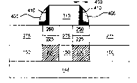
400:I形接触结构 405:氧化层400: I-shaped contact structure 405: oxide layer
410:L形导电结构 450:导电结构厚度410: L-shaped conductive structure 450: Thickness of conductive structure
500:绝缘材料 600:存储材料500: insulation material 600: storage material
700:顶导电构件 750:字符线宽度700: top conductive member 750: character line width
800:基底 810、820:掺杂硅区800:
830:底导电构件或位线 840:接触插塞830: bottom conductive member or bit line 840: contact plug
850:I形接触结构 855:L形接触结构850: I-shaped contact structure 855: L-shaped contact structure
860:存储材料 870:字符线860: storage material 870: character line
具体实施方式 Detailed ways
以下将详细说明本发明的较佳实施例,其实例表示于附图中;而在附图及说明文中,相同或相似的部分已尽可能以相同或相似的标记来标示。另外,请注意所有附图皆已经过简化,其尺寸比例并不一定精确。同时,为方便清楚地描述本实施例,下文中使用如顶、底、左、右、上、下、在上、在下、前、后等方位用词以说明附图所示的结构,这些方位用词不应被解释成是在以任何方式限制本发明的范围。Preferred embodiments of the present invention will be described in detail below, examples of which are shown in the drawings; and in the drawings and description, the same or similar parts are marked with the same or similar symbols as much as possible. In addition, please note that all drawings are simplified, and their scales may not be exact. Meanwhile, in order to describe this embodiment clearly, words such as top, bottom, left, right, upper, lower, upper, lower, front, and rear are used hereinafter to illustrate the structure shown in the accompanying drawings. The words should not be construed as limiting the scope of the invention in any way.
虽然本说明书提及特定的附图实施例,但其仅为范例而非限制,亦即,下文虽仅讨论实施例,但其却可被解释成是涵盖上述这些实施例的变形例、替代例及等同例,只要其在权利要求所界定的本发明范围内。另请了解此处所述的工艺步骤与结构并未涵盖制作存储材料单元的完整制造流程。本发明亦可与业界常用的各种IC制造技术一同施行,但其中只有可令本发明更容易了解的常用工艺步骤才有其说明。一般来说,本发明在半导体元件与工艺的领域皆有其应用性,然而为作清楚的说明,下文主要说明的是相变存储材料等存储材料、存储单元,以及主动面积较小的I形或L形接触结构的制造方法。Although this specification refers to specific embodiments of the drawings, they are only examples and not limiting. That is, although only embodiments are discussed below, they can be interpreted as covering modifications and alternatives to these embodiments. and equivalents, as long as they are within the scope of the present invention defined by the claims. Please also understand that the process steps and structures described here do not cover the complete manufacturing process for making memory material units. The present invention can also be implemented with various IC manufacturing techniques commonly used in the industry, but only the common process steps that can make the present invention easier to understand are described. Generally speaking, the present invention has its applicability in the fields of semiconductor elements and processes. However, for a clear description, the following mainly describes storage materials such as phase-change storage materials, storage cells, and I-shaped semiconductors with smaller active areas. Or the manufacturing method of the L-shaped contact structure.
请进一步参照附图,图1~3为本发明的背景技术,图4A及4B为本发明实施例的存储单元的立体图,图5的流程图用以说明制造I形及L形接触结构的存储单元的发明步骤,其中接触结构由导电材料或存储材料制成。这些步骤表示于图7~25B中,但图25A/B的结构以晶体管作为存取元件,而非二极管。Please further refer to accompanying drawings, Fig. 1~3 is the background technology of the present invention, Fig. 4A and 4B are the perspective view of the memory unit of the embodiment of the present invention, the flow chart of Fig. 5 is used for explaining the memory of manufacturing I shape and L shape contact structure Inventive step of the unit, wherein the contact structure is made of a conductive material or a memory material. These steps are shown in Figures 7-25B, but the structures of Figures 25A/B use transistors as access elements instead of diodes.
请参照图1,其为晶片10(例如是半导体晶片)的平面图,其上可能形成有一或多个集成电路,且可分割为多个IC晶方12,其将可被封装成IC芯片。图2为包含存储元件的基板的示意方框图,此存储元件位于晶方12的部分区域中,且此晶方12可包含IC存储器。存储器14可包括一或多个存储阵列20。此表示的存储阵列20以导线18连接至控制电路16。此控制电路16选择图3所示的适当的行及列坐标以存取存储阵列20,而得以进行读写。Please refer to FIG. 1 , which is a plan view of a chip 10 (such as a semiconductor chip), on which one or more integrated circuits may be formed, and may be divided into a plurality of IC dies 12, which may be packaged into IC chips. FIG. 2 is a schematic block diagram of a substrate including memory elements located in a partial area of a die 12 , which may include an IC memory. Memory 14 may include one or more memory arrays 20 . The memory array 20 shown here is connected to the control circuit 16 by wires 18 . The control circuit 16 selects the appropriate row and column coordinates shown in FIG. 3 to access the memory array 20 for reading and writing.
图3为依本发明实施例的方法所制作的存储单元所构成的图2存储单元阵列20的一部分的电路简图。存储单元阵列20基本上包括许多存储单元22,其一般排列成垂直的列与行,其中每一行存储单元22基本上共用一电连接,即一个位24;每一列存储单元22基本上共用一电连接,即一条字符线26。在典型的实施方式中,每一位元线24由底导电构件形成,且每一字符线26由预导电构件形成。如此领域所知者,图2的控制电路16选择对应的列与行坐标来启动对应的存取元件,藉此读写每一个存储单元22。此存取元件可能包括晶体管或二极管。FIG. 3 is a schematic circuit diagram of a part of the memory cell array 20 in FIG. 2 composed of memory cells manufactured by the method according to an embodiment of the present invention. The memory cell array 20 basically includes a plurality of memory cells 22, which are generally arranged in vertical columns and rows, wherein each row of memory cells 22 basically shares an electrical connection, that is, a bit 24; each column of memory cells 22 basically shares an electrical connection. connection, that is, a character line 26 . In an exemplary embodiment, each bit line 24 is formed from a bottom conductive member, and each word line 26 is formed from a pre-conductive member. As known in the art, the control circuit 16 of FIG. 2 selects the corresponding column and row coordinates to activate the corresponding access element, thereby reading and writing each memory cell 22 . The access element may include a transistor or a diode.
图5为本发明实施例的存储单元形成方法的流程图。此实施例采用由导电或存储材料制成的I形或L形接触结构,且以二极管作为存取元件。FIG. 5 is a flowchart of a method for forming a memory cell according to an embodiment of the present invention. This embodiment uses an I-shaped or L-shaped contact structure made of conductive or memory material, and uses a diode as the access element.
步骤30开始即提供底导电构件,其依后续操件来看可称为位线。以图5方法制造的存储单元的实施例显示于图4A,其中底导电构件200作为位线。形成此底导电构件200(步骤30)的工艺步骤表示于图6~9中。
步骤35形成存取元件,其在所示实施例中由第一层掺杂硅材225与第二层掺杂硅材250所构成的二极管存取元件,且其形成步骤表示于图10~15中。
接着,材质可包括导电材料的I形接触结构400可以步骤40~65形成,其表示于图16~18及19A、20A、21A中。在I形接触结构400形成后,即以步骤70~75形成存储材料与顶导电构件(即字符线)。举例来说,如下文将详细说明者,在于支撑结构上沉积导电材料(例如呈薄膜状)的步骤50及后续步骤55~65完成之后,步骤70形成存储材料或硫族材料等相变型存储材料600,如图22A所示。接着,步骤75沉积顶导电构件700的材料,如图23A所示。形成导电材料的I形导电结构400的另一选择,则是如步骤80~100般形成材质包括存储材料的I形接触结构,其并未详细绘于附图中。Next, the I-shaped
步骤105为图24表示的蚀刻步骤,其图案化/蚀刻底导电构件200以上的各层,以形成字符线与存储单元。Step 105 is an etching step shown in FIG. 24 , which patterns/etches layers above the bottom
图4B是与图4A相似的立体图,除其中I形导电结构400以L形导电结构410代替之外。图4B即为表示图5方法所制造的存储单元的另一实施例,其一开始即形成底导电构件200(步骤30),如图6~9所示。接着如同图4A的实施例,形成第一层掺杂硅材225与第二层掺杂硅材250以构成二极管存取元件(步骤35),如图10~15所示。步骤40~65形成L形导电结构410,如图16~18及19B、19C、20B、21B所示,其材质例如包括导电材料。接着,步骤70形成存储材料或硫族材料等相变型存储材料600,如图22B所示,下一步骤75则沉积顶导电构件700的材料,如图23B所示。再者,如同I形接触结构400的情形,L形接触结构410亦可依步骤80~100改以存储材料或相变材料形成,而非导电材料。接着,进行图24表示的蚀刻步骤(步骤105),图案化/蚀刻底导电构件200以上的各层,以形成字符线与存储单元。FIG. 4B is a perspective view similar to FIG. 4A , except that the I-shaped
底导电构件与二极管存取元件的形成步骤以图6~15为辅作说明。特别是,图6为其上沉积有第一氧化层150(如二氧化硅层)的半导体基板148的剖面图,图7则表示图6结构中第一氧化层150的多个部分以公知光刻蚀刻工艺选择性去除,而形成沟渠175的情形。图8表示图7结构在第一层导电材料以公知方法形成后的情形,其中底导电构件200形成在第一氧化层150内(步骤30)。此导电材料例如可包括硅、复晶硅、钨、铜、铝铜合金、铝硅铜合金或其组合,或是其它类似材料。The steps of forming the bottom conductive member and the diode access element are illustrated with reference to FIGS. 6-15 . In particular, FIG. 6 is a cross-sectional view of a
图9表示图8结构中第一层导电材料的多个部分以回蚀法或CMP去除,而裸露出第一氧化层150的上表面(步骤30)的情形。此步骤产生可作为存储阵列的位线的底导电构件200。FIG. 9 shows the situation in which portions of the first layer of conductive material in the structure of FIG. 8 are removed by etch-back or CMP, exposing the upper surface of the first oxide layer 150 (step 30). This step produces bottom
请参照图10,接着在底导电构件200上形成第一层掺杂硅材225(步骤35),再如图11所示,于第一层掺杂硅材225上形成第二层掺杂硅材250(步骤35)。在所示实施例中,第一层掺杂硅材225的材质包括N-掺杂硅,其掺质浓度例如约1015~1017/cm3;而第二层掺杂硅材250的材质包括P+掺杂硅,其掺质浓度例如约1018~1020/cm3。Please refer to FIG. 10, and then form a first layer of doped
请参照图12,其表示图11结构中第二层与第一层掺杂硅材250与225被蚀刻成二极管存取元件(步骤35)的情形,此存取元件与底导电构件200操作性地接触。在修改的实施例中,亦可以N/P/金属(225/250/200)结构取代上述P/N/金属(250/225/200)结构。P或N掺杂硅的掺杂浓度可变化以得高整流比(rectification ratio)及高电流密度,并使其两端可有低接触电阻。虽然此处所示为二极管,但在修改的实施例中亦可适用其它存取元件,例如是金属氧化物半导体(MOS)元件等,但不限于此。Please refer to FIG. 12, which shows the second layer and the first layer of doped
图13为图12结构的俯视图,而图12为图13的12-12’剖面图。接着如图14所示,在蚀刻后的第一层与第二层掺杂硅材225与250上形成一层第二氧化材料275(步骤35),其例如是包括以CVD形成的二氧化硅。接下来可对图14结构进行CMP或回蚀工艺,以移除第二氧化材料275至第二层掺杂硅材250露出为止,藉以形成图15的结构。Fig. 13 is a top view of the structure in Fig. 12, and Fig. 12 is a cross-sectional view along line 12-12' of Fig. 13 . Next, as shown in FIG. 14 , a layer of
请参照图16,接着在第二层掺杂硅材250与第一氧化层225二者上方形成垫材料层300(步骤40),其材质例如可包括二氧化硅、氮化硅或一些其它的氧化物或非氧化物材料。在一实施例中,垫材料层300的材质可包括以CVD形成的二氧化硅。Referring to FIG. 16, a
图17表示图16结构的垫材料层300以光刻蚀刻步骤图案化(步骤45)后的情形。垫材料层300被图案化为支撑结构310,其在之后用于I形或L形接触结构的形成。支撑结构310包括操作性地于第二层掺杂硅材250的顶面上方延伸的侧壁。FIG. 17 shows the situation after the
图18表示依照本发明一实施例,在图17结构的支撑结构310上形成薄膜层395(步骤50与比较步骤80)。支撑结构310的侧壁直接用以形塑I形或L形的接触结构,因此不需要任何掩膜层来定义接触结构。此方法亦可提供更佳的电流密度控制性,例如,电流密度可在L形接触结构的足部降低。此薄膜层395的材质可包括导电材料(步骤50),或是薄膜存储材料或相变材料(比较步骤80)。FIG. 18 shows the formation of a
接着,蚀刻薄膜层395以形成图19A的结构(步骤55与比较步骤85),其除去薄膜层395的多个水平部分,以在支撑结构310上形成导电间隙壁(或I形接触结构)400,其厚度标记为450。移去薄膜层395的水平部分的蚀刻工艺可能包括各向异性蚀刻工艺,其所用的蚀刻剂对薄膜层395的选择性高于第二氧化材料275、支撑结构310与第二掺杂硅材250。在图19A的实施例中,接触结构的尺寸450至少有部分依薄膜层395的厚度而定。依照一实施例,薄膜层395可以溅镀或CMP法来沉积。此例举的工艺可精确地控制薄膜层395的厚度450,其方法例如是调整沉积时间。Next, the
图19B显示本发明的形成导电间隙壁或L形接触结构的实施例中,将氧化层405形成在图18结构的薄膜层395上所得结构的同一剖面图。此氧化层405的材质例如可包括四乙基硅氧烷(TEOS)-二氧化硅。依照一实施例,此氧化层405均匀地形成在该结构几乎所有的暴露表面上。FIG. 19B shows the same cross-sectional view of the structure obtained by forming the
图19C表示图19B结构经过蚀刻序列而得氧化物间隙壁及L形接触结构410的情形,其中蚀刻序列包括一或多次的各向异性蚀刻。各向异性蚀刻可以垂直方向进行,以除去氧化层405(图19B)的水平部分,而留下覆盖薄膜层395的垂直部分及部分较低水平部分的氧化物间隙壁。此蚀刻序列例如包含两次各向异性蚀刻:在第一次各向异性蚀刻时,可使用对氧化层405的选择性高于薄膜层395的蚀刻剂,其中例如可变化压力及功率以垂直加速离子,而无偏斜角。在蚀刻后,留下的氧化物间隙壁即具圆化或弯曲状,而可用以在后续蚀刻中定义L形接触结构,其中薄膜层395的暴露出部分全被除去。接着,在第二次各向异性蚀刻时,可使用对薄膜层395的选择性高于氧化物间隙壁、支撑结构310与第二氧化层275的蚀刻剂,以形成L形接触结构410。另一种选择则是此蚀刻序列仅包括单一各向异性蚀刻步骤,其除去氧化层405与薄膜层395的多个部分,且其所用蚀刻剂对氧化层405与薄膜层395的选择性高于支撑结构310与第二氧化层275。另外,控制每一L形接触结构410的足部长度的方法,例如是控制氧化层405的厚度与/或该蚀刻序列的各向异性程度或其它相关特性。FIG. 19C shows the oxide spacer and L-shaped
在可视为片状接触窗(blade contact)的I形及L形接触结构二者的典型实施例中,侧壁厚度450可约为0.1~1000纳米,而在一实例中可为100纳米。图18的薄膜层395的材质可包括导电材料,如钛、钨、氮化钛、钛钨合金、硅化钛(TixSiy)、氮化钛铝(TixAlyNz)或其组合,或是其它类似材料。In typical embodiments of both I-shaped and L-shaped contact structures, which may be considered blade contacts, the
在I形或L形接触结构以存储材料形成的修改实施例中,相似的流程可能包括在支撑结构上沉积存储材料,再以类似前述的工艺蚀刻此存储材料,以形成定义I形或L形接触结构的存储材料侧壁。典型实施例的存储材料例如可包括锗、锑及碲(如Ge2Sb2Te5),其以溅镀工艺形成在支撑结构310上方,且其厚度(450)为0.1~1000纳米,而在一实例中约为200纳米。In a modified embodiment where the I-shaped or L-shaped contact structure is formed with memory material, a similar flow may include depositing the memory material on the support structure, and then etching the memory material in a process similar to that described above to form the defined I-shape or L-shape Storage material sidewalls of the contact structure. The storage material of the typical embodiment may include germanium, antimony and tellurium (such as Ge 2 Sb 2 Te 5 ), which is formed on the
以上两种形态的沉积薄膜层皆与第二层掺杂硅材250的顶面操作性地接触,而另一选择则是通过接触插塞840与晶体管存取元件810操作性地连接,如图25A与25B所示。The above two types of deposited thin film layers are all in operative contact with the top surface of the second
图20A表示在图19A结构的支撑结构310、I形接触结构400、第二掺杂硅材250及第二氧化材料275上方形成一层绝缘材料500(步骤60与比较步骤90)的情形。此绝缘材料500例如可包括TEOS-氧化硅、SOG、BPSG或SiO2。20A shows the formation of a layer of insulating
在图21A中,图20A结构的表面以CMP工艺平坦化,直到支撑结构310的上表面暴露出为止。在一实施例中,CMP可在I形或L形接触窗的上端刚暴露出时即停止,而得很小的接触面。然而,由于接触面大小会因接触结构的倾斜状部分的CMP损失而变化,故接触尺寸可能不易控制。因此,在表示的实施例中,CMP进行到I形接触结构400的上端被完全磨平,而形成大致与支撑结构310的顶面平行的平坦面为止(步骤65与比较步骤95)。此种以化学机械研磨而得均匀宽度的结构的工艺可提供更佳的尺寸控制性。在修改的实施例中,CMP可在上述两种情形之间的中间位置处停止,以调整I形接触结构400上端的截面积。In FIG. 21A, the surface of the structure of FIG. 20A is planarized by a CMP process until the upper surface of the
图20B表示在图19C结构的支撑结构310、L形接触结构410与第二氧化材料275上形成一层绝缘材料500的情形。此绝缘材料500可能包括前述的相同材料,而后续CMP工艺亦可使用前述相同技术,以产生图21B的结构。FIG. 20B shows the situation where a layer of insulating
图22A表示在图21A结构的I形接触结构400、支撑结构310及绝缘材料500上沉积存储材料600(步骤70及比较步骤100)的情形。如此沉积的存储材料600即可与导电材料的I形接触结构400的顶面操作性地接触。每一接触面的面积,亦即I形接触结构400与存储材料600的界面面积可加以控制,尤其是以I形接触窗400的厚度450(图19A)及字符线宽度750(图24)来控制。由本发明的一面向来看,此面积可以前述方法加以控制,而可较公知者小很多。在典型的实施例中,存储材料600例如可由锗、锑及碲形成,如Ge2Sb2Te5,其可以溅镀工艺来沉积,且厚度约为0.1~1000纳米,而在一实例中约为200纳米。FIG. 22A shows the deposition of
图22B表示与图22A相似的结构,但其却具有L形接触结构410。此图表示在图21B结构的L形接触结构410、支撑结构310及绝缘材料500的暴露出表面上沉积存储材料600的情形。存储材料600可能包括以前述方法形成的前述材料。如此沉积的存储材料600即可与导电材料的L形接触结构410的顶面操作性接触。如同I形接触结构400的情形,由L形接触结构410与存储材料600的界面所定义的每一个接触面的面积可以某些方法调整,特别是以控制L形接触结构410的厚度450(图19C)与字符线宽度750(图24)的方法。FIG. 22B shows a structure similar to that of FIG. 22A but with an L-shaped
在图22A与22B的形成存储材料的实施例中,存储材料600形成在导电材料的I形与/或L形接触结构上方;而与其不同的本发明其它实施方式在存储材料的I形与/或L形接触结构上方形成导电材料(步骤100)。在此实施方式中,绝缘材料(500)沉积在I形或L形接触结构上方(步骤90),其后进行任一种上述的CMP工艺(步骤95)。步骤100的形成在存储材料的I形或L形接触结构上方的导电材料(600)例如可包括钛、钨、氮化钛、钛钨合金、硅化钛(TixSiy)、氮化钛铝(TixAlyNz)或其组合,或是其它类似材料。在典型的实施例中,导电材料可包括以溅镀法沉积的钨,其厚度约10nm至1000nm,而在一实例中为400nm。22A and 22B in the embodiment of forming the storage material, the
图23A表示在图22A结构上形成一层导电材料700的情形,其可包括复晶硅、钨、铜、铝铜合金、铝硅铜合金或其组合,或是其它类似材料。在典型的实施例中,导电材料700可包括以溅镀法沉积的钨,其厚度约10nm至1000nm。图23B则表示在图22B结构上形成一层导电材料的情形,其可以前述方法形成。FIG. 23A shows the situation of forming a layer of
图24为图23A结构经蚀刻(步骤105)后,在垂直的另一剖面上的剖面图,亦即,对应图24的剖面线与图13的12-12’垂直。另外,图23B结构经蚀刻(步骤105)后亦可得与图24类似的剖面结构。Fig. 24 is a sectional view of the structure in Fig. 23A after etching (step 105), on another vertical section, that is, the section line corresponding to Fig. 24 is perpendicular to 12-12' in Fig. 13 . In addition, after the structure in FIG. 23B is etched (step 105 ), a cross-sectional structure similar to that in FIG. 24 can also be obtained.
通过图23A与23B结构的蚀刻步骤,顶导电构件或字符线即可自行对准I形或L形接触结构400或410,其中蚀刻停止在底导电构件200的上表面,而形成字符线与存储单元。在不使用存取元件的修改实施例中,蚀刻可以连续进行至通过I形或L形接触结构400或410为止,或可持续进行而通过底导电构件。23A and 23B structure etching steps, the top conductive member or word line can self-align I-shaped or L-shaped
依照典型的实施例,顶导电构件700的宽度750约可介于10纳米到1微米之间;而在一实例中则约为200nm。字符线宽度750决定了I形与L形接触结构400与410的主动面积的第二尺寸。在此种实施例中,接触结构的主动面积即等于字符线宽度750与接触结构厚度450的乘积。所属技术领域的技术人员应可了解,此处所述的控制顶面主动面积的厚度450与宽度750的方法可用以形成截面积相对小的I形及L形接触结构。例如,当薄膜层的宽度450约25nm且宽度750约100nm时,每一I形或L形接触结构的截面主动面积即约2500nm2。此面积对应圆形接触结构的约60nm的直径,或是正方形接触结构的约50nm的宽度。因此,本发明的方法可得的接触面积明显地小于公知多种方法所得者,故其光刻工艺限制较少。According to typical embodiments, the width 750 of the top
图25A与25B表示以晶体管而非二极管作为存取元件的替代实施例。特别是,图25A的立体图显示包含晶体管以作为存取元件或操控构件形成I形接触结构的实施例。此存储单元的构件即包括顶导电构件或字符线870、存储材料860、I形接触结构850、接触插塞840、底导电构件或位线830、掺杂硅区820与810,以及基底800。同样地,图25B的立体图显示包含晶体管以作为存取元件或操控构件的形成L形接触结构的实施例。此存储单元的构件即包括顶导电构件或字符线870、存储材860、L形接触结构855、接触插塞840、底导电构件或位线830、掺杂硅区820与810,以及基底800。Figures 25A and 25B show an alternative embodiment using transistors instead of diodes as access elements. In particular, the perspective view of FIG. 25A shows an embodiment including a transistor as an access element or steering member forming an I-shaped contact structure. The components of the memory cell include top conductive member or word line 870 ,
综上所述,所属技术领域的技术人员应可了解本发明的方法可使半导体元件更容易形成,此种元件一般是只读存储元件,而特别是在集成电路中使用相变材料的只读存储元件。In summary, those skilled in the art should understand that the method of the present invention can make semiconductor elements easier to form, such elements are generally read-only memory elements, and especially read-only memory elements using phase-change materials in integrated circuits storage element.
虽然本发明已以较佳实施例披露如上,然其并非用以限定本发明,任何所属技术领域的技术人员,在不脱离本发明的精神和范围内,当可作些许的更动与改进,因此本发明的保护范围当视权利要求所界定者为准。Although the present invention has been disclosed above with preferred embodiments, it is not intended to limit the present invention. Any person skilled in the art may make some changes and improvements without departing from the spirit and scope of the present invention. Therefore, the scope of protection of the present invention should be defined by the claims.
Claims (30)
Applications Claiming Priority (2)
| Application Number | Priority Date | Filing Date | Title |
|---|---|---|---|
| US10/985,480 | 2004-11-10 | ||
| US10/985,480 US7135727B2 (en) | 2004-11-10 | 2004-11-10 | I-shaped and L-shaped contact structures and their fabrication methods |
Publications (2)
| Publication Number | Publication Date |
|---|---|
| CN1783455A CN1783455A (en) | 2006-06-07 |
| CN100383954C true CN100383954C (en) | 2008-04-23 |
Family
ID=36316883
Family Applications (1)
| Application Number | Title | Priority Date | Filing Date |
|---|---|---|---|
| CNB2005101155674A Expired - Lifetime CN100383954C (en) | 2004-11-10 | 2005-11-04 | Memory element and array, method for manufacturing contact structure, and manufactured device and element |
Country Status (2)
| Country | Link |
|---|---|
| US (2) | US7135727B2 (en) |
| CN (1) | CN100383954C (en) |
Cited By (1)
| Publication number | Priority date | Publication date | Assignee | Title |
|---|---|---|---|---|
| CN103296050A (en) * | 2012-03-02 | 2013-09-11 | 中芯国际集成电路制造(上海)有限公司 | Phase change memory and manufacturing method thereof |
Families Citing this family (18)
| Publication number | Priority date | Publication date | Assignee | Title |
|---|---|---|---|---|
| KR100568543B1 (en) * | 2004-08-31 | 2006-04-07 | 삼성전자주식회사 | Manufacturing method of phase change memory device having small contact point |
| US7687830B2 (en) * | 2004-09-17 | 2010-03-30 | Ovonyx, Inc. | Phase change memory with ovonic threshold switch |
| JP2007200963A (en) * | 2006-01-24 | 2007-08-09 | Hitachi Ltd | Semiconductor memory device |
| TW200802840A (en) * | 2006-06-15 | 2008-01-01 | Ind Tech Res Inst | Phase-change memory cell structures and methods for fabricating the same |
| KR100749740B1 (en) * | 2006-08-01 | 2007-08-17 | 삼성전자주식회사 | Manufacturing Method of Phase Change Memory Device |
| TWI305042B (en) * | 2006-08-16 | 2009-01-01 | Ind Tech Res Inst | Phase-change memory devices and methods for fabricating the same |
| US7616472B2 (en) * | 2006-10-23 | 2009-11-10 | Macronix International Co., Ltd. | Method and apparatus for non-volatile multi-bit memory |
| KR100825767B1 (en) * | 2006-12-05 | 2008-04-29 | 한국전자통신연구원 | Phase change memory device and manufacturing method thereof |
| US7767994B2 (en) * | 2006-12-05 | 2010-08-03 | Electronics And Telecommunications Research Institute | Phase-change random access memory device and method of manufacturing the same |
| TW200847399A (en) * | 2007-05-21 | 2008-12-01 | Ind Tech Res Inst | Phase change memory device and method of fabricating the same |
| TWI336128B (en) * | 2007-05-31 | 2011-01-11 | Ind Tech Res Inst | Phase change memory devices and fabrication methods thereof |
| DE102008032067A1 (en) * | 2007-07-12 | 2009-01-15 | Samsung Electronics Co., Ltd., Suwon | Method for forming phase change memories with lower electrodes |
| TW200943595A (en) * | 2008-04-03 | 2009-10-16 | Ind Tech Res Inst | Phase change memory and method for fabricating the same |
| KR101486984B1 (en) * | 2008-10-30 | 2015-01-30 | 삼성전자주식회사 | Resistance changeable memory device and method of forming thereof |
| KR20130017647A (en) * | 2011-08-11 | 2013-02-20 | 삼성전자주식회사 | Method of fabricating resistance variable memory device |
| US9691981B2 (en) | 2013-05-22 | 2017-06-27 | Micron Technology, Inc. | Memory cell structures |
| CN105551518B (en) * | 2016-01-07 | 2018-09-25 | 中国科学院上海微系统与信息技术研究所 | A kind of SOI single-port SRAMs unit and preparation method thereof |
| US9761662B1 (en) | 2017-02-03 | 2017-09-12 | Globalfoundries Inc. | Active area shapes reducing device size |
Citations (6)
| Publication number | Priority date | Publication date | Assignee | Title |
|---|---|---|---|---|
| US5825046A (en) * | 1996-10-28 | 1998-10-20 | Energy Conversion Devices, Inc. | Composite memory material comprising a mixture of phase-change memory material and dielectric material |
| US6127224A (en) * | 1997-12-31 | 2000-10-03 | Stmicroelectronics, S.R.L. | Process for forming a non-volatile memory cell with silicided contacts |
| CN1352808A (en) * | 1999-03-25 | 2002-06-05 | 能源变换设备有限公司 | Electrically programmable memory element with improved contacts |
| US20040037179A1 (en) * | 2002-08-23 | 2004-02-26 | Se-Ho Lee | Phase-changeable devices having an insulating buffer layer and methods of fabricating the same |
| CN1506973A (en) * | 2002-12-13 | 2004-06-23 | ض� | Phase change memory and producing method thereof |
| US6777705B2 (en) * | 1997-05-09 | 2004-08-17 | Micron Technology, Inc. | X-point memory cell |
Family Cites Families (9)
| Publication number | Priority date | Publication date | Assignee | Title |
|---|---|---|---|---|
| DE4213945A1 (en) * | 1991-04-29 | 1992-11-05 | Micron Technology Inc | Memory capacitor in semiconductor device for DRAM cells - comprises conductively doped poly:silicon@ layers and insulating layer comprising capacitor dielectric adjacent to memory node of 2nd poly:silicon@ layer |
| US5814527A (en) * | 1996-07-22 | 1998-09-29 | Micron Technology, Inc. | Method of making small pores defined by a disposable internal spacer for use in chalcogenide memories |
| KR100209724B1 (en) * | 1996-08-21 | 1999-07-15 | 구본준 | Flash memory and method of manufacturing the same |
| US6015977A (en) * | 1997-01-28 | 2000-01-18 | Micron Technology, Inc. | Integrated circuit memory cell having a small active area and method of forming same |
| IT1292337B1 (en) * | 1997-05-20 | 1999-01-29 | Sgs Thomson Microelectronics | STRUCTURE OF A NON VOLATILE SEMICONDUCTOR MEMORY DEVICE |
| US6031287A (en) * | 1997-06-18 | 2000-02-29 | Micron Technology, Inc. | Contact structure and memory element incorporating the same |
| US6429064B1 (en) * | 2000-09-29 | 2002-08-06 | Intel Corporation | Reduced contact area of sidewall conductor |
| US6514788B2 (en) * | 2001-05-29 | 2003-02-04 | Bae Systems Information And Electronic Systems Integration Inc. | Method for manufacturing contacts for a Chalcogenide memory device |
| US6847535B2 (en) * | 2002-02-20 | 2005-01-25 | Micron Technology, Inc. | Removable programmable conductor memory card and associated read/write device and method of operation |
-
2004
- 2004-11-10 US US10/985,480 patent/US7135727B2/en not_active Expired - Lifetime
-
2005
- 2005-11-04 CN CNB2005101155674A patent/CN100383954C/en not_active Expired - Lifetime
-
2006
- 2006-10-10 US US11/545,988 patent/US7371604B2/en not_active Expired - Lifetime
Patent Citations (6)
| Publication number | Priority date | Publication date | Assignee | Title |
|---|---|---|---|---|
| US5825046A (en) * | 1996-10-28 | 1998-10-20 | Energy Conversion Devices, Inc. | Composite memory material comprising a mixture of phase-change memory material and dielectric material |
| US6777705B2 (en) * | 1997-05-09 | 2004-08-17 | Micron Technology, Inc. | X-point memory cell |
| US6127224A (en) * | 1997-12-31 | 2000-10-03 | Stmicroelectronics, S.R.L. | Process for forming a non-volatile memory cell with silicided contacts |
| CN1352808A (en) * | 1999-03-25 | 2002-06-05 | 能源变换设备有限公司 | Electrically programmable memory element with improved contacts |
| US20040037179A1 (en) * | 2002-08-23 | 2004-02-26 | Se-Ho Lee | Phase-changeable devices having an insulating buffer layer and methods of fabricating the same |
| CN1506973A (en) * | 2002-12-13 | 2004-06-23 | ض� | Phase change memory and producing method thereof |
Cited By (2)
| Publication number | Priority date | Publication date | Assignee | Title |
|---|---|---|---|---|
| CN103296050A (en) * | 2012-03-02 | 2013-09-11 | 中芯国际集成电路制造(上海)有限公司 | Phase change memory and manufacturing method thereof |
| CN103296050B (en) * | 2012-03-02 | 2015-10-14 | 中芯国际集成电路制造(上海)有限公司 | Phase transition storage and manufacture method thereof |
Also Published As
| Publication number | Publication date |
|---|---|
| US20060099795A1 (en) | 2006-05-11 |
| CN1783455A (en) | 2006-06-07 |
| US20070032012A1 (en) | 2007-02-08 |
| US7135727B2 (en) | 2006-11-14 |
| US7371604B2 (en) | 2008-05-13 |
Similar Documents
| Publication | Publication Date | Title |
|---|---|---|
| CN100383954C (en) | Memory element and array, method for manufacturing contact structure, and manufactured device and element | |
| CN113196490B (en) | Three-dimensional NAND memory device including dual-terminal selector and method of using and manufacturing the same | |
| CN113196484B (en) | Three-dimensional ferroelectric memory array including integrated gate selector and method of forming the same | |
| US10991759B2 (en) | Methods of forming vertical field-effect transistor with selfaligned contacts for memory devices with planar periphery/array and intermediate structures formed thereby | |
| US7687796B2 (en) | Method and apparatus for forming an integrated circuit electrode having a reduced contact area | |
| US6836423B2 (en) | Single level metal memory cell using chalcogenide cladding | |
| US6673700B2 (en) | Reduced area intersection between electrode and programming element | |
| US6597009B2 (en) | Reduced contact area of sidewall conductor | |
| US6514805B2 (en) | Trench sidewall profile for device isolation | |
| CN100456513C (en) | Phase changeable memory cells and methods of forming the same | |
| US6015977A (en) | Integrated circuit memory cell having a small active area and method of forming same | |
| US6605527B2 (en) | Reduced area intersection between electrode and programming element | |
| US8592797B2 (en) | Variable resistance memory device having reduced bottom contact area and method of forming the same | |
| US7804086B2 (en) | Phase change memory device having decreased contact resistance of heater and method for manufacturing the same | |
| US20200194668A1 (en) | Interfacial resistive memory gate stack transistor cell and methods of manufacturing the same | |
| US20090242865A1 (en) | Memory array with diode driver and method for fabricating the same | |
| CN115552607B (en) | Memory array including memory cell strings and method for forming memory array including memory cell strings | |
| CN112447716A (en) | Vertical transistor array and method of forming a vertical transistor array | |
| CN113544849A (en) | Integrated circuit system, DRAM circuit system, method for forming integrated circuit system and method for forming DRAM circuit system | |
| US9343674B2 (en) | Cross-point memory utilizing Ru/Si diode | |
| US10516105B2 (en) | Resistive memory device containing oxygen-modulated hafnium oxide material and methods of making thereof | |
| TWI280635B (en) | Memory element, array of memory cell, method of forming contact structure and apparatus and semiconductor device produced by the method |
Legal Events
| Date | Code | Title | Description |
|---|---|---|---|
| C06 | Publication | ||
| PB01 | Publication | ||
| C10 | Entry into substantive examination | ||
| SE01 | Entry into force of request for substantive examination | ||
| C14 | Grant of patent or utility model | ||
| GR01 | Patent grant | ||
| CX01 | Expiry of patent term |
Granted publication date: 20080423 |
|
| CX01 | Expiry of patent term |