CN100334746C - Luminescent array, wavelength-converting sealing material and light source - Google Patents
Luminescent array, wavelength-converting sealing material and light source Download PDFInfo
- Publication number
- CN100334746C CN100334746C CNB008014957A CN00801495A CN100334746C CN 100334746 C CN100334746 C CN 100334746C CN B008014957 A CNB008014957 A CN B008014957A CN 00801495 A CN00801495 A CN 00801495A CN 100334746 C CN100334746 C CN 100334746C
- Authority
- CN
- China
- Prior art keywords
- fluorescent material
- ray
- material mixture
- garnet
- component
- Prior art date
- Legal status (The legal status is an assumption and is not a legal conclusion. Google has not performed a legal analysis and makes no representation as to the accuracy of the status listed.)
- Expired - Lifetime
Links
Images


Classifications
-
- C—CHEMISTRY; METALLURGY
- C09—DYES; PAINTS; POLISHES; NATURAL RESINS; ADHESIVES; COMPOSITIONS NOT OTHERWISE PROVIDED FOR; APPLICATIONS OF MATERIALS NOT OTHERWISE PROVIDED FOR
- C09K—MATERIALS FOR MISCELLANEOUS APPLICATIONS, NOT PROVIDED FOR ELSEWHERE
- C09K11/00—Luminescent, e.g. electroluminescent, chemiluminescent materials
- C09K11/08—Luminescent, e.g. electroluminescent, chemiluminescent materials containing inorganic luminescent materials
- C09K11/77—Luminescent, e.g. electroluminescent, chemiluminescent materials containing inorganic luminescent materials containing rare earth metals
-
- H—ELECTRICITY
- H10—SEMICONDUCTOR DEVICES; ELECTRIC SOLID-STATE DEVICES NOT OTHERWISE PROVIDED FOR
- H10H—INORGANIC LIGHT-EMITTING SEMICONDUCTOR DEVICES HAVING POTENTIAL BARRIERS
- H10H20/00—Individual inorganic light-emitting semiconductor devices having potential barriers, e.g. light-emitting diodes [LED]
- H10H20/80—Constructional details
- H10H20/85—Packages
- H10H20/851—Wavelength conversion means
- H10H20/8511—Wavelength conversion means characterised by their material, e.g. binder
- H10H20/8512—Wavelength conversion materials
-
- C—CHEMISTRY; METALLURGY
- C09—DYES; PAINTS; POLISHES; NATURAL RESINS; ADHESIVES; COMPOSITIONS NOT OTHERWISE PROVIDED FOR; APPLICATIONS OF MATERIALS NOT OTHERWISE PROVIDED FOR
- C09K—MATERIALS FOR MISCELLANEOUS APPLICATIONS, NOT PROVIDED FOR ELSEWHERE
- C09K11/00—Luminescent, e.g. electroluminescent, chemiluminescent materials
- C09K11/08—Luminescent, e.g. electroluminescent, chemiluminescent materials containing inorganic luminescent materials
- C09K11/77—Luminescent, e.g. electroluminescent, chemiluminescent materials containing inorganic luminescent materials containing rare earth metals
- C09K11/7766—Luminescent, e.g. electroluminescent, chemiluminescent materials containing inorganic luminescent materials containing rare earth metals containing two or more rare earth metals
- C09K11/7767—Chalcogenides
- C09K11/7769—Oxides
-
- C—CHEMISTRY; METALLURGY
- C09—DYES; PAINTS; POLISHES; NATURAL RESINS; ADHESIVES; COMPOSITIONS NOT OTHERWISE PROVIDED FOR; APPLICATIONS OF MATERIALS NOT OTHERWISE PROVIDED FOR
- C09K—MATERIALS FOR MISCELLANEOUS APPLICATIONS, NOT PROVIDED FOR ELSEWHERE
- C09K11/00—Luminescent, e.g. electroluminescent, chemiluminescent materials
- C09K11/08—Luminescent, e.g. electroluminescent, chemiluminescent materials containing inorganic luminescent materials
- C09K11/77—Luminescent, e.g. electroluminescent, chemiluminescent materials containing inorganic luminescent materials containing rare earth metals
- C09K11/7766—Luminescent, e.g. electroluminescent, chemiluminescent materials containing inorganic luminescent materials containing rare earth metals containing two or more rare earth metals
- C09K11/7774—Aluminates
-
- H—ELECTRICITY
- H05—ELECTRIC TECHNIQUES NOT OTHERWISE PROVIDED FOR
- H05B—ELECTRIC HEATING; ELECTRIC LIGHT SOURCES NOT OTHERWISE PROVIDED FOR; CIRCUIT ARRANGEMENTS FOR ELECTRIC LIGHT SOURCES, IN GENERAL
- H05B33/00—Electroluminescent light sources
- H05B33/12—Light sources with substantially two-dimensional radiating surfaces
- H05B33/14—Light sources with substantially two-dimensional radiating surfaces characterised by the chemical or physical composition or the arrangement of the electroluminescent material, or by the simultaneous addition of the electroluminescent material in or onto the light source
-
- H—ELECTRICITY
- H10—SEMICONDUCTOR DEVICES; ELECTRIC SOLID-STATE DEVICES NOT OTHERWISE PROVIDED FOR
- H10H—INORGANIC LIGHT-EMITTING SEMICONDUCTOR DEVICES HAVING POTENTIAL BARRIERS
- H10H20/00—Individual inorganic light-emitting semiconductor devices having potential barriers, e.g. light-emitting diodes [LED]
- H10H20/80—Constructional details
- H10H20/85—Packages
- H10H20/851—Wavelength conversion means
- H10H20/8511—Wavelength conversion means characterised by their material, e.g. binder
- H10H20/8512—Wavelength conversion materials
- H10H20/8513—Wavelength conversion materials having two or more wavelength conversion materials
-
- H10W72/884—
-
- H10W74/00—
-
- H10W90/756—
Landscapes
- Chemical & Material Sciences (AREA)
- Inorganic Chemistry (AREA)
- Engineering & Computer Science (AREA)
- Materials Engineering (AREA)
- Organic Chemistry (AREA)
- Luminescent Compositions (AREA)
- Led Device Packages (AREA)
- Optical Filters (AREA)
Abstract
本发明推荐一种通过射线源激励的荧光材料混合物,其采用具有用Ce激活的石榴石结构A3B5O12的荧光材料,在此第一组分A含有由Y,Lu,Sc,La,Gd、Sm和Tb组成的组中的至少一种元素,并且包含Tb作为主晶格构造,而第二组分B代表元素Al,Ga或In中的至少一种,并且混合荧光材料中的多种。此外推荐了相应的波长转换的浇注料和所属的光源装置。
This invention recommends a fluorescent material mixture excited by a radiation source, employing a fluorescent material having a Ce-activated garnet structure A3B5O12 . Here, the first component A contains at least one element from the group consisting of Y, Lu, Sc, La, Gd, Sm, and Tb, and includes Tb as the main lattice structure. The second component B represents at least one element from Al, Ga, or In, and multiple elements of the fluorescent material are mixed. Furthermore, a corresponding wavelength-converting casting material and a corresponding light source device are recommended.
Description
技术领域technical field
本发明涉及一种荧光材料混合物,一种所属的波长转换的浇注料和一种所属的光源装置。The invention relates to a phosphor mixture, an associated wavelength-converting casting compound and an associated light source arrangement.
本发明尤其是涉及通过蓝色或近紫外光谱范围中波长激励用的,发射黄色或黄绿色的一种石榴石荧光材料混合物。尤其是安排了含有荧光材料混合物的一种浇注树脂基体作为浇注料,和尤其是安排了与荧光材料混合物或与浇注料结合的一种发光二极管作为光源。In particular, the invention relates to a garnet phosphor mixture emitting yellow or yellow-green for excitation by wavelengths in the blue or near-ultraviolet spectral range. In particular, a casting resin matrix containing a phosphor mixture is provided as potting compound, and in particular a light-emitting diode combined with the phosphor compound or potting compound is provided as light source.
背景技术Background technique
从WO 98/05078中公开了光源用的一种荧光材料和一种所属的光源。在那里采用具有A3B5O12:D结构的石榴石作为荧光材料,在此石榴石上第一组分由不同稀土金属中的至少一种组成,组分B由元素Al,Ga或In中的一种组成。掺杂物D为铈(Ce)。A fluorescent material for a light source and an associated light source are disclosed from WO 98/05078. There, garnets with the structure A3B5O12:D are used as fluorescent material, on the garnets the first component consists of at least one of the different rare earth metals, and the component B consists of one of the elements Al, Ga or In. Dopant D is cerium (Ce).
从WO 97/50132中公开了一种类似的荧光材料,在此荧光材料上要么采用Ce,要么采用铽(Tb)作为掺杂物。Ce在黄色光谱范围发射,而Tb在绿色光谱范围发射。在两种情况下采用与发射蓝色的光源结合的荧光材料用于实现白的混合色。A similar fluorescent material is disclosed from WO 97/50132, on which either Ce or terbium (Tb) is used as a dopant. Ce emits in the yellow spectral range, while Tb emits in the green spectral range. In both cases phosphors are used in combination with a blue-emitting light source for the realization of the white mixed color.
从WO 98/12757中公开了基于由上述文献中公开的荧光材料和透明浇注基体的,波长转换的浇注料。在此通过引用(Rückbezug)吸纳此文献的公布内容。From WO 98/12757 a wavelength-converting casting compound based on the fluorescent material disclosed in the above-mentioned document and a transparent casting matrix is disclosed. The publication of this document is hereby incorporated by reference (Rückbezug).
在例如按WO 97/50132生成白的混合光时,通过合适的选择,即通过荧光材料的组成,荧光材料的颗粒大小和荧光材料的浓度来改变此白色光的色温或色品位置是已知的,通过引用尤其是涉及浇注料的组成和涉及浇注料的制造的WO 97/50132的公布内容同样是本说明的内容。在基于这些参数的情况下却只能以比较大的工作量优化所生成白色光的色调(CIE比色图表中的色品位置X和Y)的优化。这一点尤其是适用于位于坐标CIEX=0.33和CIEY=0.33上的所谓的消色差点或“等能点”。When generating white mixed light, for example according to WO 97/50132, it is known to change the color temperature or chromaticity position of this white light by suitable selection, i.e. by composition of the fluorescent material, particle size of the fluorescent material and concentration of the fluorescent material Yes, by reference especially the publication of WO 97/50132 relating to the composition of castables and to the manufacture of castables is likewise the content of this description. On the basis of these parameters, however, the optimization of the hue of the generated white light (chromaticity positions X and Y in the CIE color chart) can only be optimized with a comparatively large workload. This applies in particular to the so-called achromatic points or “isoenergy points” at the coordinates CIEX=0.33 and CIEY=0.33.
此外从较好的彩色再现角度通过光谱中的较高的红色成分来优化荧光材料是费事的。Furthermore, it is complex to optimize phosphors with a higher red component in the spectrum from the point of view of better color rendering.
最后从荧光材料的吸收峰值角度针对朝发光源发射峰值方向来优化荧光材料是困难的。Finally, it is difficult to optimize the fluorescent material for the emission peak direction towards the light emitting source from the perspective of the absorption peak of the fluorescent material.
发明内容Contents of the invention
因此本发明的任务在于,说明开始时所述方式的一种荧光材料混合物,在以优化参数为基础的条件下可以迅速而简单地制造此荧光材料混合物,并且此荧光材料混合物是适合于所属的波长转换的浇注料以及所属的光源的。It is therefore the object of the present invention to specify a phosphor mixture of the type described at the outset, which can be produced quickly and simply under optimized parameters and which is suitable for the associated Castables for wavelength conversion and associated light sources.
根据本发明的具有不同成分的荧光材料混合物,其用于把来自于射线源的射线部分地或全部地转换成较长波的射线,其中所述荧光材料中的至少一种材料具有用Ce激活的石榴石结构A3B5O12,在此第一组分A含有元素Y,Lu,Sc,La,Gd、Sm和Tb中的至少一种元素,并且包含Tb作为主晶格构造,而第二组分B含有元素Al,Ga和In中的至少一种元素。A mixture of fluorescent materials with different compositions according to the invention for partially or completely converting radiation from a radiation source into longer-wave radiation, wherein at least one of the fluorescent materials has a Ce-activated Garnet structure A 3 B 5 O 12 , where the first component A contains at least one of the elements Y, Lu, Sc, La, Gd, Sm and Tb, and contains Tb as the main lattice structure, while the second The binary component B contains at least one of the elements Al, Ga and In.
按本发明尤其是优先对于其发射位于短波光谱范围中的,尤其是优先在蓝色光谱范围中的,或在紫外光谱范围中的光源采用具有多种荧光材料的荧光材料混合物。这些荧光材料尤其拥有用铈掺杂的石榴石结构A3B5O12:D,第一组分A在此含有元素Y、Lu、Sc、La、Gd、Sm和Tb中的至少一种元素,而第二组分含有元素Al,Ga和In中的至少一种元素。According to the invention, phosphor mixtures with several phosphors are used preferably for light sources whose emission is in the short-wave spectral range, especially preferentially in the blue spectral range, or in the ultraviolet spectral range. These phosphors have in particular a garnet structure A 3 B 5 O 12 :D doped with cerium, the first component A here containing at least one of the elements Y, Lu, Sc, La, Gd, Sm and Tb , while the second component contains at least one of the elements Al, Ga and In.
在开始时所述文献中说明了所述荧光材料的制造和作用方式。在此尤其值得一提的是,在大约400和500nm之间的光谱范围中激励时作为主晶格的、即石榴石第一组分的组成部分的铽(Tb)是适合于发射黄色光的,其掺杂物为铈的荧光材料的。以前除此铈之外曾推荐铽作为绿色光谱范围中发射用的激活剂(Aktivator)的。单独采用铽,或共同与上面推荐的其它稀土金属中的至少一种作为石榴石第一组分的主要组成部分是可能的。The production and mode of operation of the fluorescent materials are described at the outset. It is particularly worth mentioning here that terbium (Tb), which is a constituent of the host lattice, i.e. a constituent of the first component of garnet, is suitable for yellow emission when excited in the spectral range between approximately 400 and 500 nm , whose dopant is cerium fluorescent material. Terbium has previously been recommended in addition to cerium as an activator for emission in the green spectral range. It is possible to use terbium alone, or together with at least one of the other rare earth metals recommended above, as the main component of the first component of garnet.
特别优先采用(Tb1-x-ySExCey)3(Al,Ga)5O12结构的石榴石,在此适用Particular preference is given to garnets of the structure (Tb 1-xy SE x Ce y )3(Al,Ga) 5 O 12 , where applicable
SE=Y,Gd,La,Sm和/或Lu;SE=Y, Gd, La, Sm and/or Lu;
0≤x≤0.5-y;0≤x≤0.5-y;
0<y<0.1。0<y<0.1.
采用元素Al或Ga中的至少一种作为第二组分(B)。第二组分B可能附加地含有In。激活剂是铈。At least one of the elements Al or Ga is used as the second component (B). The second component B may additionally contain In. The activator is cerium.
这些荧光材料吸收具有在420nm至490nm之间范围中的波长的电磁射线,并且因对于蓝色光源的,尤其是半导体LED的射线可以激励这些荧光材料。GaN基上的,或InGaN基上的LED半导体芯片是优先适合的,这些LED半导体芯片在430nm至480nm范围中的发射峰值时发射蓝色光。These phosphors absorb electromagnetic radiation having a wavelength in the range between 420 nm and 490 nm and can be excited by the radiation of blue light sources, in particular semiconductor LEDs. LED semiconductor chips on a GaN base, or on an InGaN base, which emit blue light with an emission peak in the range of 430 nm to 480 nm, are preferably suitable.
在与本发明的关联中,对于GaN或InGaN基上的发光二极管芯片原则上理解为一种发光二极管芯片,它的射线发射区具有GaN、InGaN和/或同族的氮化物,以及基于此上的混合晶体,例如像Ga(Al,In)N。In the context of the present invention, a light-emitting diode chip on a GaN or InGaN basis is understood in principle to be a light-emitting diode chip whose radiation-emitting region has GaN, InGaN and/or nitrides of the same family, and a light-emitting diode chip based thereon Mixed crystals like Ga(Al,In)N for example.
例如从Shuji Nakamura,Gerhard Fasol著:蓝色激光二极管,Springer出版社柏林,海德堡1997,209及以下页中公开了这种发光二极管芯片。Such light-emitting diode chips are disclosed, for example, from Shuji Nakamura, Gerhard Fasol: Blue Laser Diodes, Springer Verlag Berlin, Heidelberg 1997, 209 ff.
以前所述的荧光材料通过蓝色光来激励,并且在它们那方发射波长位移地位于500nm之上范围中的光。在铈激活的Tb石榴石荧光材料的情况下发射的峰值位于大约550nm上。The phosphors described above are excited by blue light and emit light from them in a wavelength-shifted range above 500 nm. In the case of cerium-activated Tb garnet phosphors, the emission peak is at approximately 550 nm.
上面说明的荧光材料在420至490nm范围中吸收,并且因此可从通过蓝色光源的射线来激励。用其峰值位于430至470nm上的,发射蓝色光的LED芯片曾达到良好的结果。Tb石榴石:Ce荧光材料的发射峰值位于大约550nm上。The fluorescent materials described above absorb in the range of 420 to 490 nm and can therefore be excited by radiation from a blue light source. Good results have been achieved with blue-emitting LED chips whose peak lies at 430 to 470 nm. The emission peak of the Tb garnet:Ce fluorescent material is located at about 550 nm.
基于发送蓝色光的LED芯片与具有含Tb石榴石的荧光材料的荧光材料混合物的组合,这种荧光材料特别适合于在发射白色光的LED元件中的用途,通过吸收LED芯片发射的一部分来激励含Tb石榴石的荧光材料,并且Tb石榴石荧光材料的发射将LED的余下的射线补充成白光。Based on the combination of an LED chip emitting blue light with a phosphor mixture with a phosphor containing Tb garnet, which is particularly suitable for use in LED components emitting white light, excited by absorbing a part of the emission of the LED chip The fluorescent material contains Tb garnet, and the emission of the Tb garnet fluorescent material supplements the remaining radiation of the LED into white light.
尤其是Ga(In)N-LED芯片,但用于在420至490nm范围中的发射生成蓝色的LED的任何另外的途径也适合于作为发射蓝色光的LED芯片。尤其是推荐发射范围430至470nm为主要的发射范围,因为效率然后是最高的。Ga(In)N-LED chips are especially suitable, but any other approach for blue-emitting LEDs emitting in the range of 420 to 490 nm is also suitable as blue-emitting LED chips. Especially the emission range 430 to 470 nm is recommended as the main emission range, since the efficiency is then highest.
荧光材料混合物的吸收和发射带位置的微调通过稀土金属的种类和量的选择是可能的。与发光二极管相结合首先位于0.25≤x≤0.5-y之间的x的范围适合在上述Tb石榴石荧光材料上的。Fine tuning of the position of the absorption and emission bands of the phosphor mixture is possible through the selection of the type and amount of the rare earth metal. In combination with light-emitting diodes, the range of x between 0.25≤x≤0.5-y is suitable for the above-mentioned Tb garnet fluorescent material.
y的特别优先的范围位于0.02<y<0.05上。A particularly preferred range for y lies at 0.02<y<0.05.
(TbxSE11-x-yCey)3(Al,Ga)5O12结构的石榴石展示作为荧光材料组分的良好适应性,在此适用SE=Y、Ga、La和/或Lu;Garnets of the (Tb x SE1 1-xy Ce y ) 3 (Al, Ga) 5 O 12 structure exhibit good suitability as components of fluorescent materials, where SE=Y, Ga, La and/or Lu are suitable;
0≤x≤0.02,尤其是x=0.01;0≤x≤0.02, especially x=0.01;
0<y<0.1。y经常位于0.01至0.05范围中。0<y<0.1. y often lies in the range 0.01 to 0.05.
在主晶格中的较小量的Tb总的首先用来改善已知的铈激活的荧光材料的性能,而可以有针对性地采用添加较大量的Tb首先用于推移已知的铈激活荧光材料的发射波长。因此高成分的Tb尤其是良好地适合于具有低于5000 K的低色温的白色LED。A smaller amount of Tb in the host lattice is generally used to improve the performance of known cerium-activated fluorescent materials, while a larger amount of Tb can be used in a targeted manner to push the known cerium-activated fluorescence The emission wavelength of the material. A high content of Tb is therefore especially well suited for white LEDs with a low color temperature below 5000 K.
众所周知,为了激励在文献中已详述的类型YAG:Ce的荧光材料采用具有430和480nm之间范围中发射峰值的,在镓氮化物或铟镓氮化物基上的发射蓝色LED。例如由Osram公司在名称L175之下销售一种这样的荧光材料。在其上部分或全部地通过上述稀土金属中的一种代替了元素钇的另外荧光材料是已知的。It is known to use blue-emitting LEDs on the basis of gallium nitride or indium gallium nitride with an emission peak in the range between 430 and 480 nm for the excitation of fluorescent materials of the type YAG:Ce detailed in the literature. Such a phosphor is sold, for example, under the designation L175 by the company Osram. Further fluorescent materials are known, on which the elemental yttrium is partially or completely replaced by one of the aforementioned rare earth metals.
在适合于按本发明荧光材料混合物的一种荧光材料上通过铽大部分地代替了钇原子。荧光材料例如可能有-以下称作为具有67%的L175/Tb的-组成[Y0.29Tb0.67Ce0.04]3Al5O5。On a phosphor suitable for the phosphor mixture according to the invention, the yttrium atoms are largely replaced by terbium. The fluorescent material may, for example, have the composition [Y 0.29 Tb 0.67 Ce 0.04 ] 3 Al 5 O 5 , hereinafter referred to as having an L175/Tb of 67%.
按本发明考虑了,通过混合具有不同组成和因此具有对于蓝色光的甚至不同吸收峰值的着色的荧光材料粉来安排荧光材料混合物的色调和色品位置。例如可以通过将荧光材料L175(纯粹的YAG:Ce)与所述种类的,在其上钇部分或全部地通过铽(L175/Tb,Tb>0%)代替的荧光材料的混合来实现这一点。混合比可以是1∶1。可是也可以采用另外的荧光材料或由此荧光材料变异的另外荧光材料代替YAG:Ce,在此额外地可以变化混合比。It is conceivable according to the invention to arrange the color tone and chromaticity position of the phosphor mixture by mixing colored phosphor powders having different compositions and thus even different absorption peaks for blue light. This can be achieved, for example, by mixing the fluorescent material L175 (pure YAG:Ce) with a fluorescent material of the said kind, on which yttrium is partially or completely replaced by terbium (L175/Tb, Tb > 0%) . The mixing ratio can be 1:1. However, instead of YAG:Ce, another fluorescent material or another fluorescent material that is a variation of this fluorescent material can also be used, whereby the mixing ratio can additionally be varied.
本发明的一个特别的优点在于,以粉末形式存在的荧光材料可以毫无问题地混合,并且因此以比较简单的方式使得在CIE比色图表上的目标色品位置的有针对性的调节成为可能。因此根据像纯粹YAG:Ce那样的石榴石结构和所采用LED的色品位置可以在比色图表上表示一束直线,这些直线中的一条穿过目标色品位置的所选择坐标。通过LED芯片和荧光装置的组合可以在色品位置直线的斜率方面容易地变化各个色品位置的合成的色品位置直线。因此生成具有LED和波长转换荧光材料的荧光装置是立即可能的,此荧光材料的合成的色品位置直线准确地穿过在色品位置图表上的坐标X=0.33和Y=0.33处的消色差点。此消色差点定义纯粹的白色。除此之外实现例如向光谱中较高的红色成分方向的,合成色谱的推移是可能的,这一般例如通过较高的L175/Tb成分导至较好的色彩再现。A particular advantage of the invention is that the phosphors present in powder form can be mixed without problems and thus enable a targeted adjustment of the position of the target chromaticity on the CIE color chart in a comparatively simple manner. . Depending on the garnet structure like pure YAG:Ce and the chromaticity position of the LEDs used, a bundle of straight lines can thus be represented on the color chart, one of these straight lines passing through the selected coordinates of the target chromaticity position. The resulting chromaticity position line for the individual chromaticity positions can easily be varied with respect to the slope of the chromaticity position line by the combination of the LED chip and the fluorescent device. It is therefore immediately possible to create a fluorescent device with an LED and a wavelength converting phosphor whose resultant chromaticity position line passes exactly through the achromatic at coordinates X=0.33 and Y=0.33 on the chromaticity position diagram Almost. This achromatic almost defines pure white. In addition, it is possible to achieve a shift in the composite color spectrum, for example in the direction of a higher red component of the spectrum, which generally leads to better color reproduction, for example, through a higher L175/Tb component.
此外按本发明考虑了,在对于所生成射线至少部分地透明的浇注料中,优先在合成材料中,特别优先地在环氧浇注树脂,硅浇注树脂,或丙烯酸盐浇注树脂中,或在这些树脂的混合物中,或在例如像无机玻璃那样的能透过射线的另外合适的材料中分散按本发明的荧光装置。为此按WO98/12757中公开的方法将按本发明的荧光装置优先制造为与浇注料和其它元素的颜料粉末混合物。Furthermore, it is conceivable according to the invention to use at least partially transparent casting materials for the radiation generated, preferably in synthetic materials, particularly preferably in epoxy casting resins, silicone casting resins, or acrylate casting resins, or in these A phosphor according to the invention is dispersed in a mixture of resins or in another suitable radiation-transparent material such as inorganic glass. For this purpose, the fluorescent device according to the invention is preferably produced as a pigment powder mixture with casting compound and other elements according to the method disclosed in WO 98/12757.
因此根据本发明的用于波长转换的浇注料,该浇注料基于透明合成材料,并包括具有不同成分的荧光材料混合物以用于把来自于射线源的射线部分地或全部地转换成较长波的射线。所述荧光材料中的至少一种材料具有用Ce激活的石榴石结构A3B5O12,在此第一组分A含有元素Y,Lu,Sc,La,Gd、Sm和Tb中的至少一种元素,并且包含Tb作为主晶格构造,而第二组分B含有元素Al,Ga或In中的至少一种元素。并且所述的荧光材料混合物是作为无机的荧光颜料粉被混合在所述的透明合成材料中的。Thus according to the invention an encapsulant for wavelength conversion which is based on a transparent synthetic material and comprises a mixture of phosphors with different compositions for the partial or complete conversion of radiation from a radiation source into longer-wave wavelengths Rays. At least one of the fluorescent materials has a Ce-activated garnet structure A 3 B 5 O 12 , where the first component A contains at least one of the elements Y, Lu, Sc, La, Gd, Sm and Tb One element, and contains Tb as the main lattice structure, and the second component B contains at least one element among the elements Al, Ga or In. And the fluorescent material mixture is mixed in the transparent synthetic material as inorganic fluorescent pigment powder.
此外按本发明安排了属于荧光装置的光源装置,在此光源装置上射线源发射光谱的蓝色范围中的或紫外范围中的射线,并且将此射线借助于按本发明的荧光装置部分或全部地转换成长波的射线,在此在部分的转换时将所转换的射线与用于生成白色混合光的射线源所发射的射线混合。Furthermore, according to the invention, a light source arrangement belonging to the fluorescent device is provided, in which the radiation source emits radiation in the blue range or in the ultraviolet range of the spectrum, and this radiation is partly or completely directed by means of the fluorescent device according to the invention The long-wave radiation is ground-converted, and the converted radiation is mixed with the radiation emitted by the radiation source for generating the white mixed light during the partial conversion.
据此,根据本发明的包含有射线源和荧光材料混合物的光源装置,在此所述的射线源发射400至500nm波长范围内的射线,所述的荧光材料混合物具有不同的成分并被安排用来接收所述的射线,其中所述荧光材料中的至少一种材料具有用Ce激活的石榴石结构A3B5O12,在此第一组分A含有元素Y,Lu,Sc,La,Gd、Sm和Tb中的至少一种元素,并且至少在部分的Tb中形成主晶格构造,而第二组分B含有元素Al,Ga和In中的至少一种元素,以及所述的射线被所述的荧光材料混合物至少部分地转换为较长波的射线。Accordingly, according to the light source device of the present invention comprising a radiation source and a mixture of fluorescent materials, the radiation source described herein emits radiation in the wavelength range of 400 to 500 nm, the mixture of fluorescent materials has different compositions and is arranged to use to receive said rays, wherein at least one of said fluorescent materials has a garnet structure A 3 B 5 O 12 activated with Ce, where the first component A contains elements Y, Lu, Sc, La, At least one element of Gd, Sm and Tb, and form a main lattice structure in at least part of Tb, while the second component B contains elements Al, at least one element of Ga and In, and said rays Longer-wave radiation is at least partially converted by the phosphor mixture.
同样地从WO98/12757中公开了具有可是仅一种荧光材料的这样的光源装置。Such a light source arrangement with possibly only one fluorescent material is likewise known from WO 98/12757.
附图说明Description of drawings
以下借助于与图1和2结合的实施例详述本发明。所展示的:The invention is described in detail below with the aid of an exemplary embodiment in conjunction with FIGS. 1 and 2 . Shown:
图1为具有不同荧光材料的和按本发明荧光装置的色品位置直线的色品位置图表,和Fig. 1 is the chromaticity position diagram with different fluorescent materials and according to the chromaticity position straight line of the fluorescent device of the present invention, and
图2为通过按本发明光源装置的实施例的示意的剖面图。2 is a schematic sectional view through an exemplary embodiment of a light source arrangement according to the invention.
具体实施方式Detailed ways
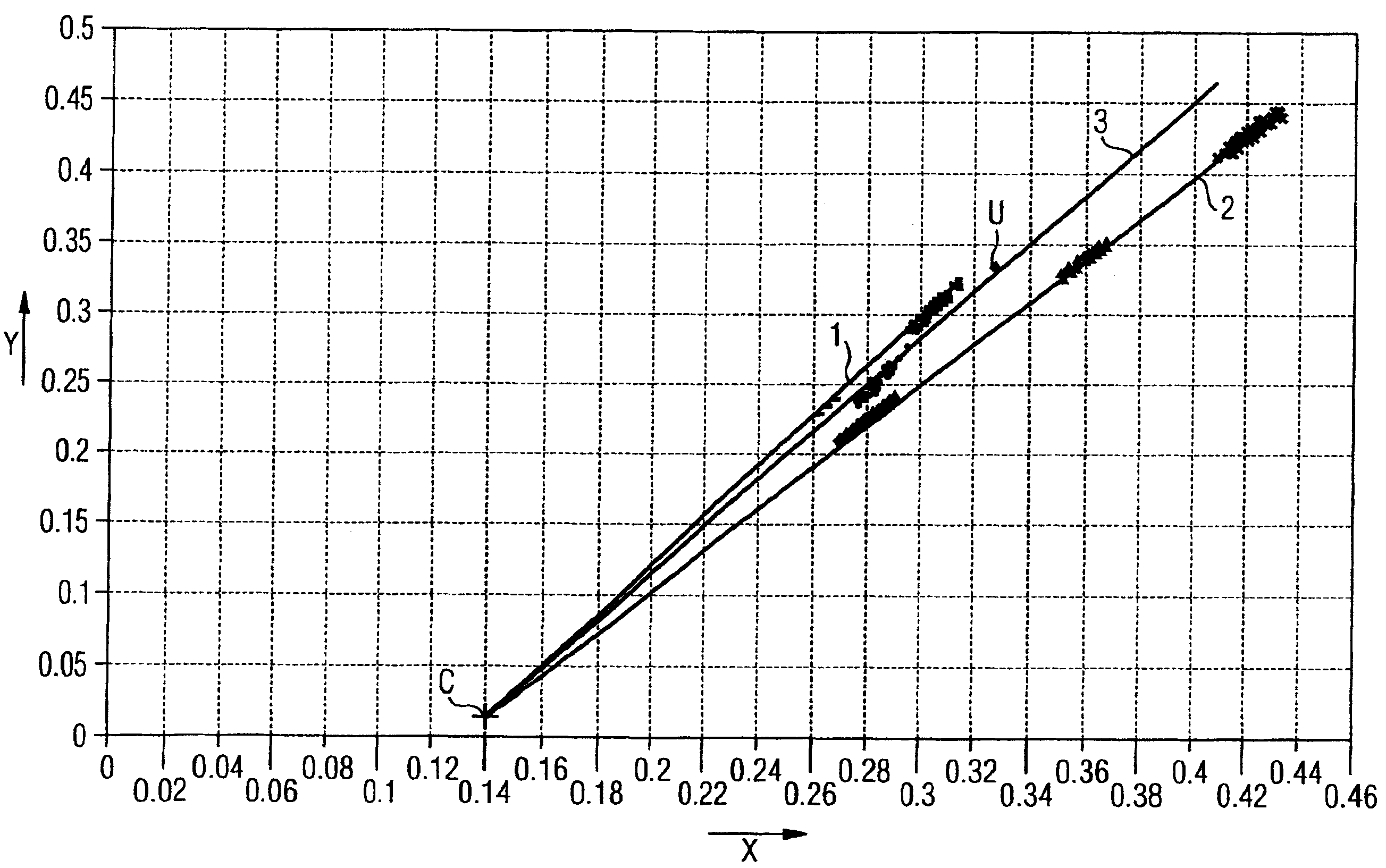
按图1表示了一种色品位置图表,此色品位置图表在横坐标上含有CIE比色图表的色品位置坐标X,和在纵坐标上含有色品位置坐标Y。FIG. 1 shows a chromaticity position diagram which contains the chromaticity position coordinate X of the CIE color chart on the abscissa and the chromaticity position coordinate Y on the ordinate.
以用于生成白色混合光的光源装置为基础,正如它例如是在WO97/50132中所说明的那样。It is based on a light source arrangement for generating white mixed light, as is described, for example, in WO 97/50132.
例如采用在蓝色光谱范围中发射的和其色品位置点相应地在色品位置图表中位于X=0.14和Y=0.02上的一种基于InGaN的LED芯片。在具有色品位置C的LED蓝色光的和例如在透明浇注料中所埋入荧光材料所发射光的混合物上产生不同的色品位置直线。For example, an InGaN-based LED chip is used which emits in the blue spectral range and whose chromaticity locus points correspond to X=0.14 and Y=0.02 in the chromaticity locus diagram. Different chromaticity position lines are produced on the mixture of the blue light of the LED having the chromaticity position C and the light emitted by the fluorescent material embedded, for example, in the transparent potting compound.
例如在采用纯粹的YAG:Ce作为荧光材料时产生色品位置直线1。在采用在其上通过铽部分或主要地代替Y的荧光材料时产生在色品位置直线1之下分布的色品位置直线。在采用具有(按上述公式的)67%的A位置上的Tb含量的荧光材料条件下,产生在图表中画入的色品位置直线2。For example, when pure YAG:Ce is used as fluorescent material, the
直线1分布在位于色品位置坐标X=0.33和Y=0.33上的消色差点U之上,而直线2分布在此消色差点U之下。在具有色品位置直线1和2的以比例1∶1的两种荧光材料的混合物上,和在埋入透明的浇注料的情况下(请参阅按图2的上面公布的实施例)像图1的图表所展示的那样产生准确穿过色品位置图表的消色差点或白点的直线3。The
以类似的方式通过尤其是具有石榴石结构的不同荧光材料的混合物获得穿过CIE比色图表的所希望的不同坐标的色品位置曲线是可能的。In a similar manner, it is possible to obtain desired chromaticity position curves of different coordinates across the CIE color chart by mixtures of different phosphors, in particular having a garnet structure.
荧光材料粉混合物是有利地埋入相应地优化的浇注料中的,在此尤其是可以优化荧光材料粉的粒度。在WO98/12757中说明了用于制造这种的波长转换浇注料的方法。The phosphor powder mixture is advantageously embedded in a correspondingly optimized potting compound, whereby in particular the particle size of the phosphor powder can be optimized. A method for producing such wavelength-converting castables is described in WO 98/12757.
在光源装置的在图2中示意地表示的特别优先的实施形式上,以GaN或InGaN为基础的发光二极管芯片10是布置在优先由合成材料制成的,射线不可透过的发光二极管基壳20的缺口11中的。In a particularly preferred embodiment of the light source device shown schematically in FIG. 2 , the GaN- or InGaN-based light-emitting
发光二极管基壳20是由芯片10的电气接头经其从壳体中引出的电气接头导线或接头引线21、22贯通的。The light-emitting
缺口11的内壁12形成由芯片10所发送光的和由荧光材料混合物所发射光的反光镜,并且向芯片10的主发射方向13偏转此光。The
缺口11是用浇注料14充填的,此浇注料14具有透明浇注树脂基质15,优先具有环氧浇注树脂或丙烯酸盐树脂(例如聚甲基丙烯酸甲脂),或具有这些树脂的混合物,所安排的荧光材料粉混合物16是混入这些树脂中的。The
荧光材料粉混合物优先含有具有粒度≤20μm的荧光材料颜料,并且含有平均颗粒直径d50≤5μm。The phosphor powder mixture preferably contains phosphor pigments having a particle size ≤ 20 μm and an average particle diameter d 50 ≤ 5 μm.
除了浇注树脂15和荧光材料颜料16之外,此外在浇注料14中优先含有着触变剂、矿物的扩散剂、疏水剂和/或增附剂。In addition to the casting
在实施例上例如涉及发射白色光的发光二极管元件,在此二极管元件中具有混合比1∶1的荧光粉L175(YAG:Ce)和L175/Tb(具有67%Tb)是含有在浇注料14中的,并且发光二极管元件所发射混合光的色品位置位于图1中所示图表的直线3上。The embodiment relates, for example, to a light-emitting diode element emitting white light, in which the phosphors L175 (YAG:Ce) and L175/Tb (with 67% Tb) with a mixing ratio of 1:1 are contained in the casting
当然借助于上述实施例的本发明的阐述自然不应看作为本发明局限于所说明特征的本身。除了由发光二极管芯片或激光二极管芯片制造的半导体本体之外,尤其是聚合物LED作为光源属于考虑之列。同样地除了纯粹的YAG:Ce之外也拥有代替Y的Lu、Sc、La、Gd以及Sm成分的荧光材料粉也属于本发明的范围。此外纳入了在其上铽成分小于上述荧光材料公式上的石榴石。The explanation of the invention with the aid of the above-described exemplary embodiments should of course not be seen as limiting the invention to the described features per se. In addition to semiconductor bodies produced from light-emitting diode chips or laser diode chips, in particular polymer LEDs come into consideration as light sources. Similarly, fluorescent material powders having Lu, Sc, La, Gd, and Sm components instead of Y in addition to pure YAG:Ce also fall within the scope of the present invention. In addition, garnets on which the terbium content is smaller than the above-mentioned fluorescent material formula are included.
按本发明的荧光装置和所属的浇注料原则上是在发光二极管元件的在WO97/50132和WO98/12757中公布的所有结构形式上可采用的。The fluorescent device according to the invention and the associated potting compound are in principle usable for all constructions of light-emitting diode components disclosed in WO 97/50132 and WO 98/12757.
Claims (21)
Applications Claiming Priority (5)
| Application Number | Priority Date | Filing Date | Title |
|---|---|---|---|
| DE19934126.5 | 1999-07-23 | ||
| DE19934126A DE19934126A1 (en) | 1999-07-23 | 1999-07-23 | Fluorescent oxide for forming white LEDs, includes cerium-activated garnet-based oxide with terbium addition |
| DE19963791.1 | 1999-12-30 | ||
| DE19963791A DE19963791A1 (en) | 1999-12-30 | 1999-12-30 | Fluorescent oxide for forming white LEDs, includes cerium-activated garnet-based oxide with terbium addition |
| PCT/DE2000/002495 WO2001009370A2 (en) | 1999-07-30 | 2000-07-28 | Detection and identification of bacterial strains |
Publications (2)
| Publication Number | Publication Date |
|---|---|
| CN1327706A CN1327706A (en) | 2001-12-19 |
| CN100334746C true CN100334746C (en) | 2007-08-29 |
Family
ID=26054272
Family Applications (1)
| Application Number | Title | Priority Date | Filing Date |
|---|---|---|---|
| CNB008014957A Expired - Lifetime CN100334746C (en) | 1999-07-23 | 2000-07-24 | Luminescent array, wavelength-converting sealing material and light source |
Country Status (10)
| Country | Link |
|---|---|
| US (3) | US7132786B1 (en) |
| EP (2) | EP1471775B9 (en) |
| JP (2) | JP3825318B2 (en) |
| KR (1) | KR100450647B1 (en) |
| CN (1) | CN100334746C (en) |
| AT (1) | ATE279089T1 (en) |
| AU (1) | AU7267500A (en) |
| CA (1) | CA2343909C (en) |
| DE (2) | DE50016032D1 (en) |
| WO (1) | WO2001008453A1 (en) |
Cited By (1)
| Publication number | Priority date | Publication date | Assignee | Title |
|---|---|---|---|---|
| CN104342156A (en) * | 2013-07-30 | 2015-02-11 | 宁波升谱光电半导体有限公司 | Fluorescent powder and preparation method thereof, and luminescent device comprising fluorescent powder |
Families Citing this family (62)
| Publication number | Priority date | Publication date | Assignee | Title |
|---|---|---|---|---|
| CN100334746C (en) * | 1999-07-23 | 2007-08-29 | 奥斯兰姆奥普托半导体股份有限两合公司 | Luminescent array, wavelength-converting sealing material and light source |
| JP4817534B2 (en) * | 2000-06-09 | 2011-11-16 | 星和電機株式会社 | Light emitting diode lamp |
| US6616862B2 (en) | 2001-05-21 | 2003-09-09 | General Electric Company | Yellow light-emitting halophosphate phosphors and light sources incorporating the same |
| US6596195B2 (en) | 2001-06-01 | 2003-07-22 | General Electric Company | Broad-spectrum terbium-containing garnet phosphors and white-light sources incorporating the same |
| DE10133352A1 (en) | 2001-07-16 | 2003-02-06 | Patent Treuhand Ges Fuer Elektrische Gluehlampen Mbh | Lighting unit with at least one LED as a light source |
| CN1311054C (en) * | 2001-07-19 | 2007-04-18 | 南帝化学工业股份有限公司 | Yttrium Aluminum Garnet Phosphor Powder and Its Preparation and Application |
| JP4032682B2 (en) * | 2001-08-28 | 2008-01-16 | 三菱化学株式会社 | Phosphor |
| JP3749243B2 (en) * | 2001-09-03 | 2006-02-22 | 松下電器産業株式会社 | Semiconductor light emitting device, light emitting apparatus, and method for manufacturing semiconductor light emitting device |
| DE10146719A1 (en) | 2001-09-20 | 2003-04-17 | Patent Treuhand Ges Fuer Elektrische Gluehlampen Mbh | Lighting unit with at least one LED as a light source |
| DE10147040A1 (en) | 2001-09-25 | 2003-04-24 | Patent Treuhand Ges Fuer Elektrische Gluehlampen Mbh | Lighting unit with at least one LED as a light source |
| US7008558B2 (en) | 2001-10-11 | 2006-03-07 | General Electric Company | Terbium or lutetium containing scintillator compositions having increased resistance to radiation damage |
| US6630077B2 (en) * | 2001-10-11 | 2003-10-07 | General Electric Company | Terbium- or lutetium - containing garnet phosphors and scintillators for detection of high-energy radiation |
| WO2003080764A1 (en) * | 2002-03-22 | 2003-10-02 | Nichia Corporation | Nitride phosphor and method for preparation thereof, and light emitting device |
| TWI226357B (en) | 2002-05-06 | 2005-01-11 | Osram Opto Semiconductors Gmbh | Wavelength-converting reaction-resin, its production method, light-radiating optical component and light-radiating semiconductor-body |
| GB2400372B (en) * | 2003-04-09 | 2005-03-23 | Photonic Materials Ltd | Single crystal scintillators |
| DE10316769A1 (en) * | 2003-04-10 | 2004-10-28 | Patent-Treuhand-Gesellschaft für elektrische Glühlampen mbH | Luminescence conversion LED used in optical semiconductor components has LED chip emitting primary radiation in specified region which is partially or completely converted into longer wavelength radiation |
| EP1659335A4 (en) | 2003-08-28 | 2010-05-05 | Mitsubishi Chem Corp | LIGHT EMITTING DEVICE AND PHOSPHORUS |
| CN100354389C (en) * | 2003-10-09 | 2007-12-12 | 中国科学院上海硅酸盐研究所 | Aluminic gadolinium-base luminescent film material chip and preparing method thereof |
| DK176137B1 (en) * | 2003-10-27 | 2006-09-25 | Danfoss Silicon Power Gmbh | Flow distribution unit and cooling unit with bypass flow |
| US7094362B2 (en) * | 2003-10-29 | 2006-08-22 | General Electric Company | Garnet phosphor materials having enhanced spectral characteristics |
| JP2005264031A (en) * | 2004-03-19 | 2005-09-29 | Kun-Chui Lee | White light-emitting device |
| JP4529544B2 (en) * | 2004-05-21 | 2010-08-25 | スタンレー電気株式会社 | LED manufacturing method |
| JP2006222288A (en) | 2005-02-10 | 2006-08-24 | Toshiba Corp | White LED and manufacturing method thereof |
| KR101388470B1 (en) * | 2005-02-28 | 2014-04-23 | 미쓰비시 가가꾸 가부시키가이샤 | Phosphor and method for production thereof, and application thereof |
| US7329907B2 (en) | 2005-08-12 | 2008-02-12 | Avago Technologies, Ecbu Ip Pte Ltd | Phosphor-converted LED devices having improved light distribution uniformity |
| JP2007165811A (en) | 2005-12-16 | 2007-06-28 | Nichia Chem Ind Ltd | Light emitting device |
| CN101385145B (en) | 2006-01-05 | 2011-06-08 | 伊鲁米特克斯公司 | Discrete optics for directing light from LEDs |
| JP4992250B2 (en) | 2006-03-01 | 2012-08-08 | 日亜化学工業株式会社 | Light emitting device |
| US7737634B2 (en) * | 2006-03-06 | 2010-06-15 | Avago Technologies General Ip (Singapore) Pte. Ltd. | LED devices having improved containment for liquid encapsulant |
| US20070269915A1 (en) * | 2006-05-16 | 2007-11-22 | Ak Wing Leong | LED devices incorporating moisture-resistant seals and having ceramic substrates |
| CN101077973B (en) | 2006-05-26 | 2010-09-29 | 大连路明发光科技股份有限公司 | Silicate fluorescent material, method for producing same, and light-emitting device using same |
| US20070295969A1 (en) * | 2006-06-26 | 2007-12-27 | Tong-Fatt Chew | LED device having a top surface heat dissipator |
| JP2008013607A (en) * | 2006-07-03 | 2008-01-24 | Fujifilm Corp | Tb-containing luminescent compound, luminescent composition containing the same and luminescent material, light-emitting element, solid-state laser device |
| US7820075B2 (en) * | 2006-08-10 | 2010-10-26 | Intematix Corporation | Phosphor composition with self-adjusting chromaticity |
| US8154191B2 (en) | 2006-08-15 | 2012-04-10 | Luming Science And Technology Group Co., Ltd. | Silicate base luminescent materials having multiple emission peaks, processes for preparing the same and light emitting devices using the same |
| US20090275266A1 (en) * | 2006-10-02 | 2009-11-05 | Illumitex, Inc. | Optical device polishing |
| US7789531B2 (en) | 2006-10-02 | 2010-09-07 | Illumitex, Inc. | LED system and method |
| JP5399252B2 (en) * | 2006-10-18 | 2014-01-29 | コーニンクレッカ フィリップス エヌ ヴェ | Lighting system and display device |
| CN101250408B (en) * | 2007-01-22 | 2011-03-23 | 罗维鸿 | Warm-white light-emitting diode and fluorescent powder having orange radiation thereof |
| KR20090085880A (en) * | 2008-02-05 | 2009-08-10 | 삼성에스디아이 주식회사 | Green phosphor for plasma display panel and plasma display panel comprising same |
| KR20100122485A (en) | 2008-02-08 | 2010-11-22 | 일루미텍스, 인크. | System and method for emitter layer shaping |
| JP5355030B2 (en) * | 2008-04-24 | 2013-11-27 | シチズンホールディングス株式会社 | LED light source and chromaticity adjustment method of LED light source |
| US7868340B2 (en) | 2008-05-30 | 2011-01-11 | Bridgelux, Inc. | Method and apparatus for generating white light from solid state light emitting devices |
| CN101330119B (en) * | 2008-07-22 | 2010-06-02 | 中国科学院长春光学精密机械与物理研究所 | A kind of preparation method of dye-activated green light-emitting diode |
| TW201034256A (en) | 2008-12-11 | 2010-09-16 | Illumitex Inc | Systems and methods for packaging light-emitting diode devices |
| US8449128B2 (en) | 2009-08-20 | 2013-05-28 | Illumitex, Inc. | System and method for a lens and phosphor layer |
| US8585253B2 (en) | 2009-08-20 | 2013-11-19 | Illumitex, Inc. | System and method for color mixing lens array |
| WO2011117791A1 (en) | 2010-03-24 | 2011-09-29 | Koninklijke Philips Electronics N.V. | Led-based lighting device comprising a plurality of luminescent materials |
| DE102010028949A1 (en) | 2010-05-12 | 2011-11-17 | Osram Gesellschaft mit beschränkter Haftung | headlight module |
| CN102082225A (en) * | 2010-10-21 | 2011-06-01 | 罗维鸿 | Warm white LED and fluorescent powder thereof |
| TWI538980B (en) * | 2011-11-29 | 2016-06-21 | 奇美實業股份有限公司 | Phosphor and light-emitting device using same |
| CN102723422B (en) * | 2011-12-31 | 2015-04-29 | 深圳市光峰光电技术有限公司 | Wavelength conversion device and light emitting device |
| JP6119739B2 (en) * | 2012-03-30 | 2017-04-26 | 宇部興産株式会社 | Ceramic composite for light conversion and light emitting device using the same |
| US9145517B2 (en) | 2012-04-17 | 2015-09-29 | General Electric Company | Rare earth garnet scintillator and method of making same |
| EP2789672B1 (en) * | 2012-05-01 | 2016-12-14 | National Institute for Materials Science | Optical material and production method therefor, and light emitting diode, optical isolator, and optical processing apparatus which use said optical material |
| TW201418695A (en) * | 2012-11-13 | 2014-05-16 | Phansco Corp | Pesticide detector |
| DE102013109313A1 (en) | 2013-08-28 | 2015-03-05 | Leuchtstoffwerk Breitungen Gmbh | Improved garnet phosphor and process for its preparation |
| US9923125B2 (en) * | 2013-11-25 | 2018-03-20 | Sichuan Sunfor Light Co., Ltd. | Method for improving defect-free rate of LED light source, phosphor powder, and LED light source |
| DE102015106995A1 (en) * | 2015-05-05 | 2016-11-10 | Osram Opto Semiconductors Gmbh | Optical heart rate sensor |
| JPWO2017169187A1 (en) * | 2016-03-31 | 2019-02-07 | ソニー株式会社 | Light source device and electronic device |
| US11592166B2 (en) | 2020-05-12 | 2023-02-28 | Feit Electric Company, Inc. | Light emitting device having improved illumination and manufacturing flexibility |
| US11876042B2 (en) | 2020-08-03 | 2024-01-16 | Feit Electric Company, Inc. | Omnidirectional flexible light emitting device |
Citations (1)
| Publication number | Priority date | Publication date | Assignee | Title |
|---|---|---|---|---|
| EP0142931A1 (en) * | 1983-10-17 | 1985-05-29 | AT&T Corp. | Visual display system utilizing high luminosity single crystal garnet material |
Family Cites Families (30)
| Publication number | Priority date | Publication date | Assignee | Title |
|---|---|---|---|---|
| JPS493629B1 (en) * | 1969-10-13 | 1974-01-28 | ||
| JPS493631B1 (en) * | 1969-10-16 | 1974-01-28 | ||
| JPS5443380B2 (en) | 1972-04-20 | 1979-12-19 | ||
| JPS5720623B2 (en) | 1972-04-20 | 1982-04-30 | ||
| GB1600492A (en) | 1977-01-19 | 1981-10-14 | Johnson Matthey Co Ltd | Luminescent materials |
| NL7707008A (en) * | 1977-06-24 | 1978-12-28 | Philips Nv | LUMINESCENCE SCREEN. |
| DE2837596A1 (en) * | 1978-08-29 | 1980-04-10 | Bosch Gmbh Robert | Row of light emitting diodes for visual indicators - esp. for displaying frequency of motor car radios, where each chip is covered by cast resin light dispersal element |
| CA1223030A (en) | 1983-04-25 | 1987-06-16 | Johannes T.C. Van Kemenade | Low-pressure mercury vapour discharge lamp |
| JPS62104893A (en) * | 1985-10-31 | 1987-05-15 | Sony Corp | Production of small particle of fluorescent substance |
| JPH07283253A (en) * | 1994-04-13 | 1995-10-27 | Sony Corp | Method for manufacturing semiconductor device |
| KR100334062B1 (en) * | 1994-10-12 | 2002-08-28 | 삼성에스디아이 주식회사 | Green light emitting phosphor and cathode-ray tube using the same |
| US5685899A (en) | 1995-07-28 | 1997-11-11 | Thiele Kaolin Company | Process for conditioning kaolin clays prior to removing impurities |
| DE19638667C2 (en) | 1996-09-20 | 2001-05-17 | Osram Opto Semiconductors Gmbh | Mixed-color light-emitting semiconductor component with luminescence conversion element |
| WO1997050132A1 (en) | 1996-06-26 | 1997-12-31 | Siemens Aktiengesellschaft | Light-emitting semiconductor component with luminescence conversion element |
| TW383508B (en) | 1996-07-29 | 2000-03-01 | Nichia Kagaku Kogyo Kk | Light emitting device and display |
| JPH10163535A (en) * | 1996-11-27 | 1998-06-19 | Kasei Optonix Co Ltd | White light emitting element |
| JPH10190066A (en) * | 1996-12-27 | 1998-07-21 | Nichia Chem Ind Ltd | Light emitting diode and LED display device using the same |
| JP3246386B2 (en) | 1997-03-05 | 2002-01-15 | 日亜化学工業株式会社 | Light emitting diode and color conversion mold member for light emitting diode |
| US5847507A (en) * | 1997-07-14 | 1998-12-08 | Hewlett-Packard Company | Fluorescent dye added to epoxy of light emitting diode lens |
| JP3546650B2 (en) * | 1997-07-28 | 2004-07-28 | 日亜化学工業株式会社 | Method of forming light emitting diode |
| US6294800B1 (en) * | 1998-02-06 | 2001-09-25 | General Electric Company | Phosphors for white light generation from UV emitting diodes |
| CN1101442C (en) * | 1998-11-23 | 2003-02-12 | 中国科学院长春物理研究所 | Green fluorescent body of rare-earth and garnet and its preparing process |
| US6669866B1 (en) * | 1999-07-23 | 2003-12-30 | Patent-Treuhand-Gesellschaft Fuer Elektrische Gluehlampen Mbh | Luminous substance for a light source and light source associates therewith |
| CN100334746C (en) * | 1999-07-23 | 2007-08-29 | 奥斯兰姆奥普托半导体股份有限两合公司 | Luminescent array, wavelength-converting sealing material and light source |
| US6552487B1 (en) * | 1999-10-27 | 2003-04-22 | Patent-Treuhand-Gesellschaft Fuer Elektrische Gluehlampen Mbh | Phosphor for light sources, and associated light source |
| DE10020465A1 (en) * | 2000-04-26 | 2001-11-08 | Osram Opto Semiconductors Gmbh | Radiation-emitting semiconductor component with luminescence conversion element |
| CA2380444A1 (en) | 2000-05-29 | 2001-12-06 | Patent-Treuhand-Gesellschaft Fuer Elektrische Gluehlampen Mbh | Led-based white-emitting illumination unit |
| US6596195B2 (en) * | 2001-06-01 | 2003-07-22 | General Electric Company | Broad-spectrum terbium-containing garnet phosphors and white-light sources incorporating the same |
| US6734465B1 (en) * | 2001-11-19 | 2004-05-11 | Nanocrystals Technology Lp | Nanocrystalline based phosphors and photonic structures for solid state lighting |
| US6765237B1 (en) * | 2003-01-15 | 2004-07-20 | Gelcore, Llc | White light emitting device based on UV LED and phosphor blend |
-
2000
- 2000-07-24 CN CNB008014957A patent/CN100334746C/en not_active Expired - Lifetime
- 2000-07-24 AT AT00960304T patent/ATE279089T1/en not_active IP Right Cessation
- 2000-07-24 DE DE50016032T patent/DE50016032D1/en not_active Expired - Lifetime
- 2000-07-24 EP EP04018028A patent/EP1471775B9/en not_active Expired - Lifetime
- 2000-07-24 EP EP00960304A patent/EP1116419B1/en not_active Expired - Lifetime
- 2000-07-24 JP JP2001513210A patent/JP3825318B2/en not_active Expired - Lifetime
- 2000-07-24 WO PCT/DE2000/002405 patent/WO2001008453A1/en not_active Ceased
- 2000-07-24 KR KR10-2001-7003756A patent/KR100450647B1/en not_active Expired - Lifetime
- 2000-07-24 CA CA2343909A patent/CA2343909C/en not_active Expired - Lifetime
- 2000-07-24 AU AU72675/00A patent/AU7267500A/en not_active Abandoned
- 2000-07-24 DE DE50008093T patent/DE50008093D1/en not_active Expired - Lifetime
- 2000-07-24 US US09/786,086 patent/US7132786B1/en not_active Expired - Lifetime
-
2004
- 2004-05-06 US US10/840,575 patent/US6998771B2/en not_active Expired - Lifetime
- 2004-11-25 JP JP2004341109A patent/JP4639351B2/en not_active Expired - Lifetime
-
2005
- 2005-12-07 US US11/296,673 patent/US7261837B2/en not_active Expired - Lifetime
Patent Citations (1)
| Publication number | Priority date | Publication date | Assignee | Title |
|---|---|---|---|---|
| EP0142931A1 (en) * | 1983-10-17 | 1985-05-29 | AT&T Corp. | Visual display system utilizing high luminosity single crystal garnet material |
Cited By (2)
| Publication number | Priority date | Publication date | Assignee | Title |
|---|---|---|---|---|
| CN104342156A (en) * | 2013-07-30 | 2015-02-11 | 宁波升谱光电半导体有限公司 | Fluorescent powder and preparation method thereof, and luminescent device comprising fluorescent powder |
| CN104342156B (en) * | 2013-07-30 | 2016-08-10 | 宁波升谱光电股份有限公司 | A kind of fluorescent material and preparation method thereof and the luminescent device containing this fluorescent material |
Also Published As
| Publication number | Publication date |
|---|---|
| ATE279089T1 (en) | 2004-10-15 |
| US7132786B1 (en) | 2006-11-07 |
| CA2343909A1 (en) | 2001-02-01 |
| EP1471775B9 (en) | 2011-04-13 |
| KR20010079911A (en) | 2001-08-22 |
| DE50016032D1 (en) | 2010-12-30 |
| JP2005101651A (en) | 2005-04-14 |
| US7261837B2 (en) | 2007-08-28 |
| EP1471775A3 (en) | 2008-05-14 |
| JP4639351B2 (en) | 2011-02-23 |
| WO2001008453A1 (en) | 2001-02-01 |
| KR100450647B1 (en) | 2004-10-01 |
| EP1116419B1 (en) | 2004-10-06 |
| EP1471775B1 (en) | 2010-11-17 |
| AU7267500A (en) | 2001-02-13 |
| DE50008093D1 (en) | 2004-11-11 |
| EP1471775A2 (en) | 2004-10-27 |
| JP3825318B2 (en) | 2006-09-27 |
| EP1116419A1 (en) | 2001-07-18 |
| US6998771B2 (en) | 2006-02-14 |
| CA2343909C (en) | 2013-04-02 |
| JP2003505583A (en) | 2003-02-12 |
| US20060133063A1 (en) | 2006-06-22 |
| US20050029929A1 (en) | 2005-02-10 |
| CN1327706A (en) | 2001-12-19 |
Similar Documents
| Publication | Publication Date | Title |
|---|---|---|
| CN100334746C (en) | Luminescent array, wavelength-converting sealing material and light source | |
| US6674233B2 (en) | Illumination unit having at least one LED as light source | |
| KR100920533B1 (en) | Lighting device having at least one LED as a light source | |
| US6501102B2 (en) | Light emitting diode (LED) device that produces white light by performing phosphor conversion on all of the primary radiation emitted by the light emitting structure of the LED device | |
| EP1339109B1 (en) | Red-deficiency compensating phosphor light emitting device | |
| US7183706B2 (en) | Led-based illumination unit | |
| US6504179B1 (en) | Led-based white-emitting illumination unit | |
| US6653765B1 (en) | Uniform angular light distribution from LEDs | |
| US6469322B1 (en) | Green emitting phosphor for use in UV light emitting diodes | |
| JP2005101651A5 (en) | ||
| US20080093979A1 (en) | Illumination System Comprising a Radiation Source and a Luminescent Material | |
| JP2005530917A (en) | Luminescent material, for example for LED | |
| WO2006135005A1 (en) | Light emitting device | |
| US20080017875A1 (en) | Yellow Emitting Phosphor And White Semiconductor Light Emitting Device Incorporating The Same | |
| CN108998024B (en) | Phosphor and light-emitting device | |
| JP2006013416A (en) | Color conversion light-emitting device including fluorescent powder having large particle diameter, method for producing the same, and resin composition used therefor | |
| JP2017533549A (en) | Light source with adjustable emission spectrum | |
| WO2004099342A1 (en) | Tb,b-based yellow phosphor, its preparation method, and white semiconductor light emitting device incorporating the same | |
| KR100684044B1 (en) | White light emitting diode and its manufacturing method | |
| Jose | Mueller-Mach et a |
Legal Events
| Date | Code | Title | Description |
|---|---|---|---|
| C06 | Publication | ||
| C10 | Entry into substantive examination | ||
| PB01 | Publication | ||
| SE01 | Entry into force of request for substantive examination | ||
| C14 | Grant of patent or utility model | ||
| GR01 | Patent grant | ||
| C56 | Change in the name or address of the patentee |
Owner name: OSRAM OPTO SEMICONDUCTORS GMBH + CO. OHG Free format text: FORMER NAME: SIEMENS AG |
|
| CP01 | Change in the name or title of a patent holder |
Address after: Regensburg, Germany Co-patentee after: PATENT-TREUHAND-GESELLSCHAFT FuR ELEKTRISCHE GLuHLAMPEN MBH Patentee after: OSRAM OPTO SEMICONDUCTORS GmbH Address before: Regensburg, Germany Co-patentee before: PATENT-TREUHAND-GESELLSCHAFT FuR ELEKTRISCHE GLuHLAMPEN MBH Patentee before: OSRAM OPTO SEMICONDUCTORS GmbH |
|
| ASS | Succession or assignment of patent right |
Owner name: OSRAM GMBH Free format text: FORMER OWNER: OSRAM OPTO SEMICONDUCTORS GMBH + CO. OHG Effective date: 20120307 Free format text: FORMER OWNER: OSRAM GMBH Effective date: 20120307 Owner name: PATRA PATENT TREUHAND Free format text: FORMER OWNER: PATENT-TREUHAND-GESELLSCHAFT FUR ELEKTRISCHE Effective date: 20120307 |
|
| C41 | Transfer of patent application or patent right or utility model | ||
| C56 | Change in the name or address of the patentee | ||
| CP01 | Change in the name or title of a patent holder |
Address after: Regensburg, Germany Co-patentee after: OSRAM AG Patentee after: OSRAM OPTO SEMICONDUCTORS GmbH Address before: Regensburg, Germany Co-patentee before: OSRAM GmbH Patentee before: OSRAM OPTO SEMICONDUCTORS GmbH |
|
| TR01 | Transfer of patent right |
Effective date of registration: 20120307 Address after: Munich, Germany Patentee after: OSRAM AG Address before: Regensburg, Germany Co-patentee before: OSRAM AG Patentee before: OSRAM OPTO SEMICONDUCTORS GmbH Effective date of registration: 20120307 Address after: Regensburg, Germany Co-patentee after: OSRAM GmbH Patentee after: OSRAM OPTO SEMICONDUCTORS GmbH Address before: Regensburg, Germany Co-patentee before: PATENT-TREUHAND-GESELLSCHAFT FuR ELEKTRISCHE GLuHLAMPEN MBH Patentee before: OSRAM OPTO SEMICONDUCTORS GmbH |
|
| CX01 | Expiry of patent term |
Granted publication date: 20070829 |
|
| CX01 | Expiry of patent term |