This project is the direct continuation of 5CC0 openCologne, and it also firmly ties into openPCIE.
The project aims to take openCologne to a new level, not only by introducing soft PCIE EndPoint core to GateMate portfolio, but also by challenging and validating the new, fully opensource nextPNR tool suite.
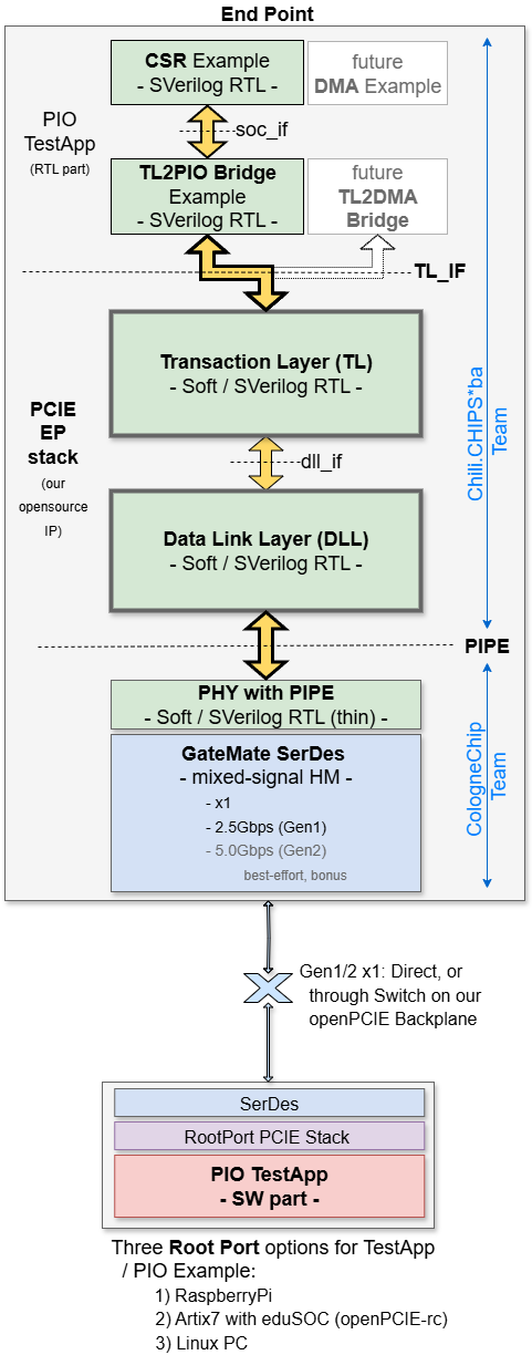
It aims to complement openPCIE RootComplex with a layered EndPoint that's portable to other FPGA families, and even to OpenROAD ASICs, leaving only the PHY in the hard-macro (HM) domain. This is the only soft PCIE protocol stack in opensource at the moment.
Our PCIE EP core comes with unique Verification IP (VIP) and two PCIE cards for GateMate. The new boards can host all three GateMate variants: A1, A2, A4 and are plug-and-play compatible with the vast assortment of 3rd-party carriers, including our opensource PCIE Backplane.
The project aims for integration with LiteX, by expanding LitePCIE portfolio, thus creating a strong foundation for the complete, end-to-end, community maintained openCompute PCIE ecosystem.
The PCIE protocol is complex. It is also bloated -- Most of the real-life users don't use most of it 😇. To be fair, our project is about creating a minimal set of features, that is a barebones design that is still interoperable with the actual PCIE HW/SW systems out there.
Its scope is therefore limited to a demonstration of the PIO writes and reads only. Other applications, such as DMA, are not in our deliverables. They can later on be added on top of the protocol stack (i.e. PCIE "core") that this project is about.
The power states and transitions are supported only to the least extent possible, and primarily in relation to the mixed-signal SerDes, which is by definition the largest consumer. Our PHY section delves into that topic.
While our commitment is to produce a Gen1 EP, the design will from the get-go support the Gen2 throughput -- We intend to, on the best-effort bases, as a bonus, try to bring up 5Gbps links. However, the procedures for automatic up- and down- training of the link speed will not be implemented.
We only support x1 (single-lane) PCIE links. The full link width training is therefore omitted, keeping only the bare minimum, as needed to wake the link up from its initial down state**
The GateMate die (A1) does not come with more than one SerDes anyway. While, in theory, a two-die A2 could support a 2-lane PCIE, that would turn everything on its head and become a major project of its own... one that would require splitting the PCIE protocol stack vertically, for implementation across two dice. Moreover, as we expect to consume most of the A1 for the PCIE stack alone, the A2 and A4 chips come into play as the banks of logic resources for the final user app.
We only support one Physical Function (PF0) and zero Virtual Functions (VF). No Traffic Classes (TC) and no Virtual Channels (VC) either.
The Configuration Space registers, while retained in our PCIE IP core, are reduced to the bare-minimum, and hard-coded for most part. The Base Address Registers (BARs) are, of course, programmable from the Root Port. We don't support 64-bit BARs, but only 32-bit, and only one address window: BAR0.
- PCIE Primer by Simon Southwell ✔
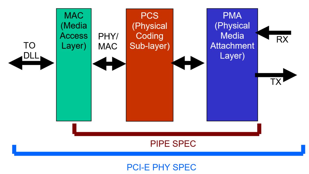
The GateMate SerDes has thus far not been used in the PCIE context. It is therefore reasonable to expect issues with physical layer, which may falter for signal integrity, jitter, or some other reason. Luckily, we have teamed up with CologneChip developers, who will own the PHY layer up to and including Physical Interface for PCI Express (PIPE) 👍. This technology-specific work is clearly separated in a directory of their own, see 2.rtl.PHY.
By adhering to PIPE architecture, we avoid mixing the generic (i.e. "logic" only) design part with FPGA-specific RTL. This does not mean that all of our RTL is portable to other vendors, but rather that it is structured in a way that facilitates future ports, with only a thin layer of code behind PIPE interface that needs to be revisited. That's a small subsection of the overall design, thereby saving a good amount of porting effort.
Reflecting on our roadmap and possible future growth paths, in addition to the aforementioned DMA and porting to other FPGA families + ASICs, we are also thinking of:
- enablement of hardware acceleration for AI, video, and general DSP compute workloads
- bolting our PCIE EP to ztachip, to then look into acceleration of the PC host Python
This borrows from Xilinx PYNQ framework and Alveo platform, where programmable DPUs are used for rapid mapping of algorithms into acceleration hardware, avoiding the time-consuming process of RTL design and validation. Such a combination would then make for the first-ever opensource "DPU" co-processor, and would also work hand-in-hand with our two new cards. After all, NiteFury and SQRL Acorn CLE 215+ M.2 cards were made for acceleration of crypto mining
- possibly also tackling the SerDes HM building brick.
-
✔ Procure Test equipment, test fixtures, dev boards and accessories
-
Create docs and diagrams that are easy to follow and comprehend
- RTL DLL and TL
- PIPE
- SW
- TB, Sim, VIP
- Design, debug and manufacture two flavors of EP cards
Given the high-speed nature of this design, we plan for two iterations:
- Slot RevA
- M.2 RevA
- Slot RevB
- M.2 RevB
- Develop opensource PHY with PIPE interface for GateMate SerDes
- x1, Gen1
- x1, Gen2 (best-effort, consider it a bonus if we make it)
-
Develop opensource RTL for PCIE EP DLL function, with PIPE interface
-
Develop opensource RTL for PCIE EP TL function
-
Create comprehensive co-sim testbench
-
Develop opensource PCIE EP Demo/Example for PIO access
- Software driver and TestApp
- Debug and bringup
- Implement it all in GateMate, pushing through PNR and timing closure
- Work with nextpnr/ProjectPeppercorn developers to identify and resolve issues
-
Port to LiteX
-
Present project challenges and achievements at (minimum) two trade fairs or conference
- FPGA Conference Europe, Munich
- Electronica, Munich
- FPGA Developer Forum, CERN
- Embedded World, Nuremberg
- ULX4M-PCIe-IO
- openPCIE Backplane
- NiteFury-and-LiteFury
- 4-port M.2 PCIE Switch
- AntMicro EMS Sim
- openEMS
The PCB part of the project shall deliver two cards: GateMate in (i) PCIE "Slot" and (ii) M.2 form-factors
While the "Slot" variant is not critical, and could have been suplanted by one of the ready-made M.2-to-Slot adapters,
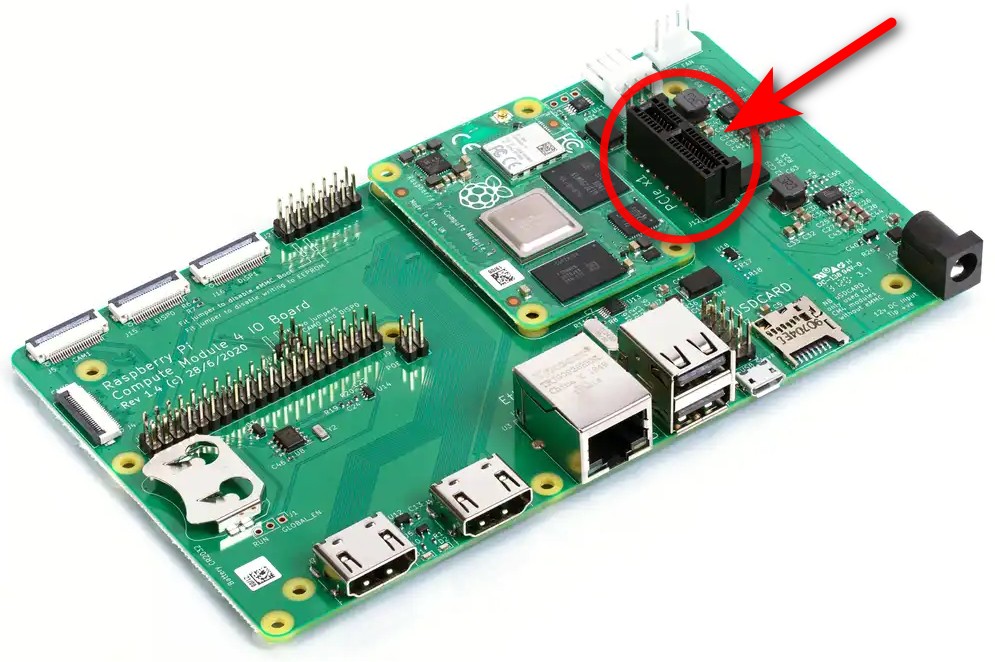
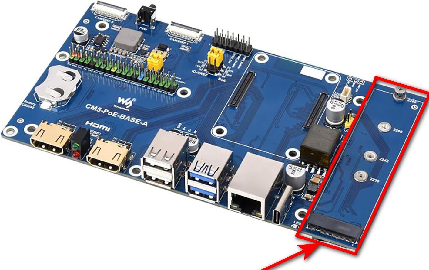
it is more practical not to have an interposer. "Slot" is still the dominant PCIE form-factor for desktops and servers. The M.2 is typically found in the laptops. Initially, we will use the existing CM4 ULX4M with off-the-shelf I/O boards:
When our two new plug-in boards become available, the plan is to gradually switch thedev platform to our openPCIE backplane, which features:
- Slots on one side
- M.2s on the other
- RootComplex also as a plug-in card (as opposed to the more typical soldered-down), for interoperability testing with RaspberryPi and Xilinx Artix-7 .
- on-board (soldered-down) PCIE Switch for interoperability testing of the most typical EP deployment scenario, which is when RootPort is not directly connected to EndPoints, but goes through a Switch.
In the final step, we intend to test them inside a Linux PC, using both "Slot" and M.2 connectivity options. For additional detail, please jump to 1.pcb/README.md
For additional detail, please jump to 2.rtl/README.md
- Using bysybox (devmem) for register access
- Yocto and Buildroot
- PCIE Utils
- Debug PCIE issues using 'lspci' and 'setpci'
The purpose of our "TestApp" is to put all hardware and software elements together, and to demonstrate how the system works in a typical end-to-end use case. The TestApp will enumerate and configure the EndPoint, then perform a series of the PIO write-read-validate transactions over PCIE, perhaps toggling some LEDs. It is envisioned as a "Getting Started" example of how to construct more complex PCIE applications.
We plan on creating not one, but three such examples, for the three representative compute platforms:
- Hard Embedded / Hosted: RaspberryPi
- Soft Embedded / BareMetal: Artix-7 FPGA acting as a RootComplex with soft on-chip RISC-V CPU
- General-purpose desktop/server class: Linux PC
The 100% baremetal (option#2) is still under investigation. While we hope to be able to write it all from scratch, given that Linux comes with such a rich set of PCIE goodies, we may end-up going with bare-Linux (i.e. minimal, specifically built by us to fit project needs), busybox, or some other clever way that works around standard Linux requirement for a hardware MMU, and it does not come with large codespace expenditure.
For additional detail, please jump to 3.sw/README.md
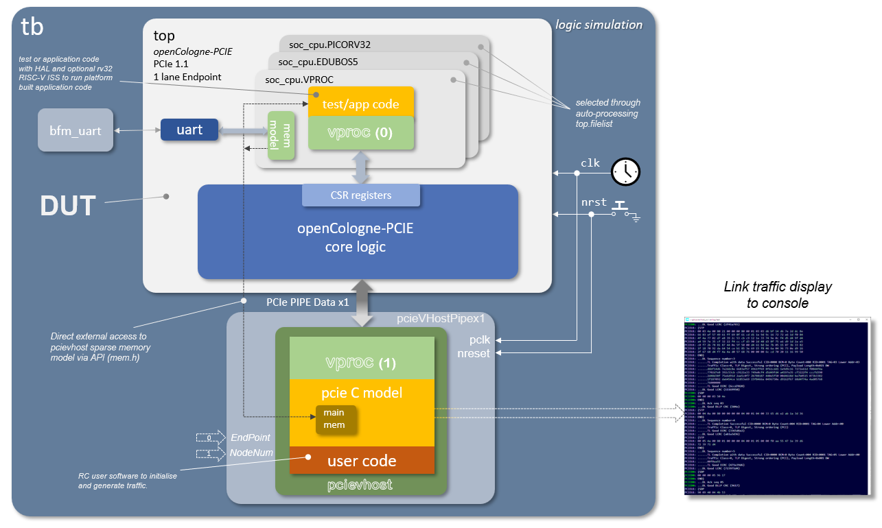
The test bench aims to have a flexible approach to simulation which allows a common test environment to be used whilst selecting between alternative CPU components, one of which uses the VProc virtual processor co-simulation element. This allows simulations to be fully HDL, with a RISC-V processor RTL implementation such as picoRV32, Ibex or eduBOS5, or to co-simulate software using the virtual processor, with a significant speed up in simulation times. The test bench has the following features:
- A VProc virtual processor based
soc_cpu.VPROCcomponent- Selectable between this or an RTL softcore
- Can run natively compiled test code
- Can run the application compiled natively with the auto-generated co-sim HAL
- Can run RISC-V compiled code using the rv32 RISC-V ISS model
- The pcieVHost VIP is used to drive the logic's PCIe link
- Uses a C sparse memory model
- An HDL component instantiated in logic gives logic access to this memory
- An API is provided to VProc running code for direct access from the pcieVHost software, which implements this sparse memory C model.
The figure below shows an overview block diagram of the test bench HDL.
More details on the architecture and usage of the test bench can be found in the README.md in the 5.sim directory.
The PCIE EP control and status register harware abstraction layer (HAL) software is auto-generated, as is the CSR RTL, using peakrdl. For co-simulation purposes an additional layer is auto-generated from the same SystemRDL specification using systemrdl-compiler that accompanies the peakrdl tools. This produces two header files that define a common API to the application layer for both the RISC-V platform and the VProc based co-simulation verification environment. The details of the HAL generation can be found in the README.md in the 4.build/ directory.
More details of the test bench, the pcievhost component and its usage can be found in the 5.sim/README.md file.
After programming the FPGA with the generated bitstream, the system was tested in a real-world environment to verify its functionality. The verification process was conducted in three main stages.
The first and most fundamental test was to confirm that the host operating system could correctly detect and enumerate the FPGA as a PCIe device. This was successfully verified on both Windows and Linux.
- On Windows, the device appeared in the Device Manager, confirming that the system recognized the new hardware.
- On Linux, the
lspcicommand was used to list all devices on the PCIe bus. The output clearly showed the Xilinx card with the correct Vendor and Device IDs, classified as a "Memory controller".
Device detected in Windows Device Manager
|
`lspci` output on Linux, identifying the device.
|
While enumeration confirms device presence, directly testing read/write functionality required an isolated environment to prevent conflicts with the host OS. A Virtual Machine (VM) with PCI Passthrough was configured for this purpose.
This step was non-trivial due to a common hardware issue: IOMMU grouping. The standard Linux kernel grouped our FPGA card with other critical system devices (like USB and SATA controllers), making it unsafe to pass it through directly.
The solution involved a multi-step configuration of the host system:
1. BIOS/UEFI Configuration
The first step was to enable hardware virtualization support in the system's BIOS/UEFI:
- AMD-V (SVM - Secure Virtual Machine Mode): This option enables the core CPU virtualization extensions necessary for KVM.
- IOMMU (Input-Output Memory Management Unit): This is critical for securely isolating device memory. Enabling it is a prerequisite for VFIO and safe PCI passthrough.
2. Host OS Kernel and Boot Configuration
A standard Linux kernel was not sufficient due to the IOMMU grouping issue. To resolve this, the following steps were taken:
- Install XanMod Kernel: A custom kernel, XanMod, was installed because it includes the necessary ACS Override patch. This patch forces the kernel to break up problematic IOMMU groups.
- Modify GRUB Boot Parameters: The kernel's bootloader (GRUB) was configured to activate all required features on startup. The following parameters were added to the
GRUB_CMDLINE_LINUX_DEFAULTline:amd_iommu=on: Explicitly enables the IOMMU on AMD systems.pcie_acs_override=downstream,multifunction: Activates the ACS patch to resolve the grouping problem.vfio-pci.ids=10ee:7014: This crucial parameter instructs the VFIO driver to automatically claim our Xilinx device (Vendor ID10ee, Device ID7014) at boot, effectively hiding it from the host OS.
3. KVM Virtual Machine Setup
With the host system properly prepared, the final step was to assign the device to a KVM virtual machine using virt-manager. Thanks to the correct VFIO configuration, the Xilinx card appeared as an available "PCI Host Device" and was successfully passed through.
This setup created a safe and controlled environment to perform direct, low-level memory operations on the FPGA without risking host system instability.
With the FPGA passed through to the VM, the final test was to verify the end-to-end communication path. This was done using the devmem utility to perform direct PIO (Programmed I/O) on the memory space mapped by the card's BAR0 register.
1. Finding the Device's Memory Address
After the FPGA is programmed and the system boots, the operating system will enumerate it on the PCIe bus and assign a memory-mapped I/O region, also known as a Base Address Register (BAR).
To find this address, you can use the lspci -v command. The image below shows the output for our target device. The key information is the Memory at ... line, which indicates the base physical address that the host system will use to communicate with the device.
In this example, the assigned base address is 0xfc500000.

Physical Address fc500000 Assigned to PCIe Device.
2. Testing Data Transfer with devmem
The devmem utility allows direct reading from and writing to physical memory addresses. We can use it to perform a simple write-then-read test to confirm that the data path to the FPGA's on-chip memory (BRAM) is working correctly.
The test procedure is as follows:
- Write a value to the device's base address.
- Read the value back from the same address to ensure it was stored correctly.
- Repeat with a different value to confirm that the memory isn't "stuck" and is dynamically updating.
The image below demonstrates this process.
- First, the hexadecimal value 0xA is written to the address 0xFC500000. A subsequent read confirms that 0x0000000A is returned.
- Next, the value is changed to 0xB. A final read confirms that 0x0000000B is returned, proving the write operation was successful.

Data Read and Write Test Using devmem.png
This test confirms that the entire communication chain is functional: from the user-space application, through the OS kernel and PCIe fabric, to the FPGA's internal memory and back.
- PCIE Sniffing
- Stark 75T Card
- ngpscope
- PCI Leech
- PCI Leech/ZDMA
- LiteX PCIE Screamer
- LiteX PCIE Analyzer
- Wireshark PCIe Dissector
- PCIe Tool Hunt
- An interesting PCIE tidbit: Peer-to-Peer communicaton. Also see this
- NetTLP - An invasive method for intercepting PCIE TLPs
We are thankful to NLnet Foundation for unreserved sponsorship of this development activity.
The wyvernSemi's wisdom and contribution mean a world of difference -- Thank you, we are honored to have you on the project!
It is in a way more important for the dev community to know about such-and-such project or IP, than for the code to exists in some repo. Without such awareness, which comes through presentations, postings, conferences, ..., the work that went into creating the technical content is not fully accomplished.
We therefore plan on putting time and effort into community outreach through multiple venues. One of them is the presence at industry fairs and conferences, such as:
This is a trade fair where CologneChip will host a booth! This trade show also features a conference track.
CologneChip is one of the sponsors and therefore gets at least 2 presentation slots.
It is very likely that CologneChip will have a booth. There is also a conference track.
CologneChip is a sponsor. They might get a few presentation slots
We are fully open to consider additional venues -- Please reach out and send your ideas!

