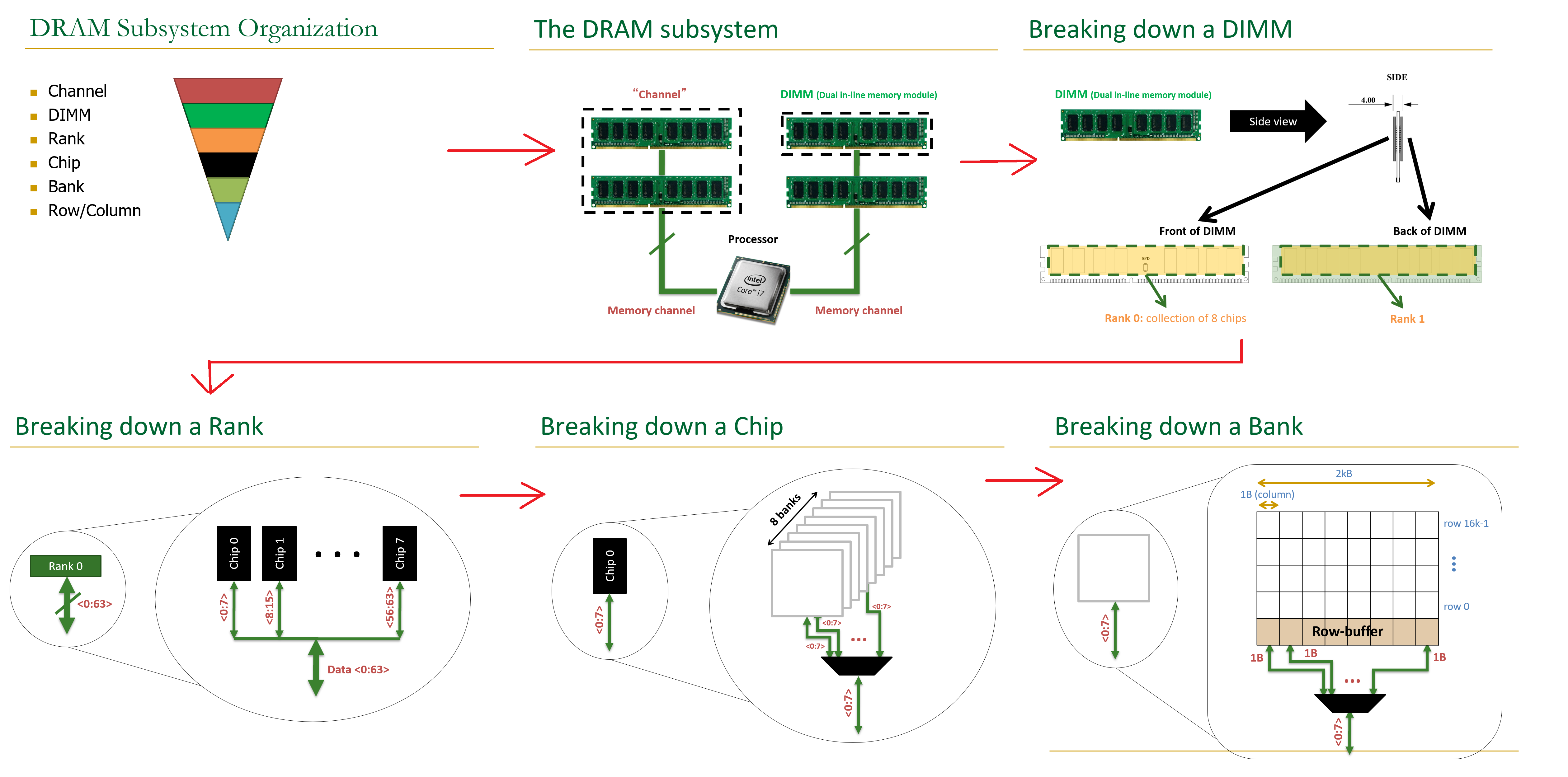
A DRAM chip contains multiple banks. A bank contains multiple DRAM rows and 1 row of sense amplifiers. A DRAM cell is composed of a capacitor and an access transistor. Only 1 row can be open in an open bank.

- Initialize
- Set 2 registers: Mode Register (latency, burst length...) and Extended Mode Register (DLL settings)
- Activate = Transferring the charge from a DRAM row to sense amp. This is destructive so the sense amp will then restore the value of the DRAM cells. Input: Bank and Row address
- Read/Write = Read/Write to a specified column. Input: Bank and Column address
- Precharge = Close current row and prepare the sense amp for next activation. The sense amp is restored to VDD/2. The DRAM cell must already be restored to its original value before precharging. Input: Bank address
Precharging charges the bit line and sense amp to VDD/2 so that reading/writing a DRAM cell is faster (the bit line needs only small charge to latch either direction). Sense amp are just SRAM cells (a D-latch with 6 CMOS so access is fast). There are other commands to refresh other rows and bank that is not used. Retention time is usually 64ms above so 64ms is used usually as the refresh time.
A refresh period is usually 64ms (32ms for higher temp since leakage is higher). If there are 8192 rows (13-bit row address), then 64ms/8192rows=7.8us/row. So a row must be refreshed EVERY 7.8us to cover all 8192 rows. Now this is a bottleneck since refresh takes time, what we can do is to access other bank while another bank is being refreshed. Refresh is essentially activate + precharge a row every 64ms. Distributed refresh is what used mostly in today's controllers than burst refresh (all rows are refreshed consecutively immediately which has long pause time). DRAM Bank is unavailable during refresh.
- Auto-refresh = The controller gives external clock
- Self-refresh = No need for external clock
In the power-down state (precharge power-down or active power-down), the DRAM still requires refresh commands to be sent to maintain the memory contents. Since no refresh operations are performed in this mode, the device may not remain in the power-down state longer than the refresh period (64ms)
Latency or delay is due to the fact that DRAM uses capacitor which induces delay.
-
Ready-to-access Latency = Activate->Read/Write. Time required to move charge from DRAM cell to sense amp before data can be read. At this time, the sense amp might not have yet restored the DRAM cell to its original value as long as the sense amp is already charged.
-
Activation Latency/tRAS= Activate->Precharge. Time required to ensure the sense amp have already restored the DRAM cell to its original value before closing the row via Precharge.
-
Precharge Latency = Precharge->Activate. Time required to restore the sense amp to "normal state" (half-VDD where it is neither 0 nor 1 but middle) before the row can be activated again
Note: The timing parameters are set for worst case, so we can reduce the timing delay slightly to optimise it further
- CPU system (@800MHZ to GHz clock frequency)
- DDR Controller
- DDR PHY = (@ ~200MHz clock frequency)
- DDR Memory inside IO_wrapper (@200MHz clock frequency)
In CPU, memory becomes bottleneck. Intel i7 is at 3GHz with 64 bit data path (192Gbit/sec). However, the DDR memory core can only work at 200MHz since higher frequency means tighter timing constraint thus lower manufacturing yield. To compensate for this low frequency, prefetching is used on the DDR memory. 2n-prefetching fetches two words at same time to be stored to internal buffer. This will then be released by the DDR memory on the positive and negative edge of clock. DDR also needs DLL (Delay-Locked Looped to align DQ to DQS) and PLL (Phase-Locked Loop used by PHY to generate input clock for DDR memory).
- {we, cas, ras} = command control
- A0-A13 = Row/Column Address Bus
- BA0-BA1 = Bank Address Bus
- DQ0-DQN = Data (Q for "output of FF, bidirectional for read/write)
- DQM = Data mask (unidirectional for write only)
- DQS = Data strobe, clock used by data (bidirectional for read/write)
- SDR don't have prefetch architecture nor DQS (only DQM for masking).
-
ODT, or On-Die Termination, is a feature used in DDR3 memory to reduce signal reflections caused by mismatched impedances on the memory bus. When ODT is activated, a resistor is placed in parallel with the memory bus to match the impedance of the bus. The ODT signal is typically driven by the memory controller and is used to control the state of the ODT resistor. A low signal in ODT corresponds to the ODT resistor being turned off (high impedance since not connected), while a high signal corresponds to the ODT resistor being turned on.
-
When the memory controller sends a write command to the memory device, it also asserts the ODT signal. This causes the ODT resistor to be placed in parallel with the memory bus, effectively matching the impedance of the bus and reducing signal reflections. By having the ODT resistor turned on during a write operation, it helps to ensure that the write data is properly received by the memory device.
-
ODT is usually turned off during read operations, but this is not because of the absence of signal reflections during read operations, but rather the ODT is turned off to minimize the noise that may be present on the memory bus and improve the signal integrity.
-
When you enable dynamic ODT, and there is no write operation, the DDR3 SDRAM terminates to a termination setting of RTT_NOM; when there is a write operation, the DDR3 SDRAM terminates to a setting of RTT_WR. You can preset the values of RTT_NOM and RTT_WR by programming the mode registers, MR1 and MR2.
-
ZQ calibration is a process used in DDR3 memory systems to adjust precisely the internal impedance of the DDR for its ODT impedances and internal buffers. The ZQ pin is linked to a highly precise external resistor, which is used for high definition adjustments of the “On” impedance of output drivers and ODT impedances.
- In write operation, the DDR memory is sampling DQ every edge of DQS (the DQS is aligned to the input clock). This means the DDR controller is tasked to shift the data so that data is stable at every clock edge.
- In read operation, the DDR memory changes the data every edge of DQS (the DQS is aligned to the input clock). This means data is stable except on the edges of the DDR memory input clock. The usual way for the DDR controller to read/sample the data is to shift the DDR controller's internal clock by 90° so it can sample the data on the middle of data eye.
- On writes, the host sends DQS phase shifted by 90 degrees and the DRAM catches DQ in the middle of its validity window (using DQS as the clock edge). On reads, the DRAM sends DQS aligned with DQ, and the host (the controller) phase-shifts DQS internally using a Delay Locked Loop (DLL) so that it can capture DQ on the middle of its data eye.

-
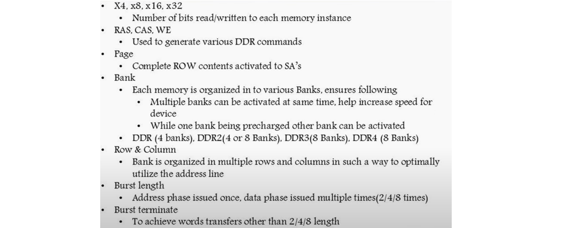
X8 means 8 bit data bus. So 4 instance of X8 will be needed to have a total of 32 bit word. X4 (8 instance), x8(4 instance), x16(2 instance)
-
In DDR3, there is no page burst unlike in SDR. Just burst lengths of 4 and 8.
-
DQS strobe is like a secondary clock used for data transfers
-
High throughput sequencing necessary in Genome analysis is limited by data movement of DRAM (memory bottleneck)
-
Core count doubling every 2 years. DRAM DIMM capacity doubling (via putting more cells in a die) every 3 years. DRAM bandwidth (xGbit/sec) trend increase slower (via increasing clock rate and pin count). Latency did not changed much in past 20 years since this is limited by capacitor physics itself.
-
LPDDR (Low Power DDR) are low power but higher latency.
-
Refresh is a big downside of DRAM. In processors, 50% of the time is wasted waiting for memory. About 40% power is wasted on DRAM due to refresh cycle.
-
Heterogenous system = A CPU core has multiple memory sources: DRAM, NVM, GPU, and more. Memory sources are different from each other and is thus "heterogenous".
-
Activation moves DRAM row charge to row buffer of Sense Amplifier. This row buffer is essentially a cache which increases hit rate if access is consecutive.
-
Rank = Consist of multiple DRAM chips to form a wide data interface (share address and command busses but provide different data, so an X8 DRAM chip will need 4 DRAM chips in 1 rank to form a 32-bit interface).
-
Channel = Different channel means a separate/different 64-bit data interface and memory controller.
-
The banks shares the address, data, and command buses.
-
With more banks, pipeline-access increases (accessing banks consecutively with least delay due to precharging+activate). With more channel, bandwidth increases since there are more data interface.
-
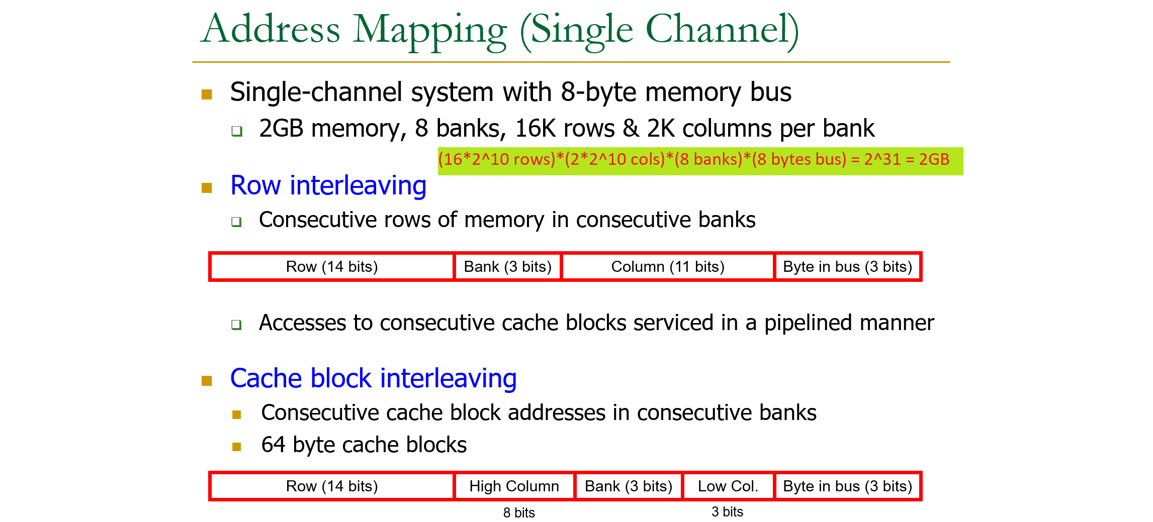
Address mapping tells how address bits are separated to row-bank-column address. Cache block interleaving is the most common one.
-
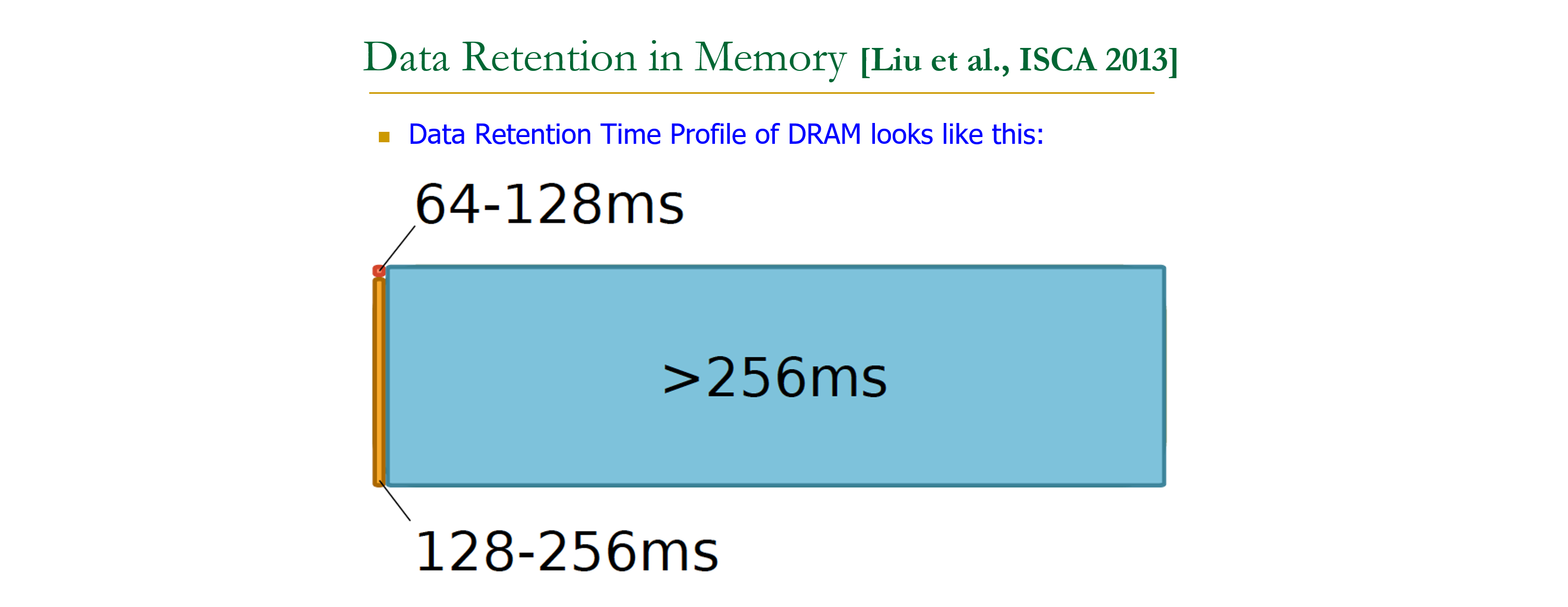
Only small percentage of data retention file is actually 64ms (<1%). More than 75% is 256ms.
-
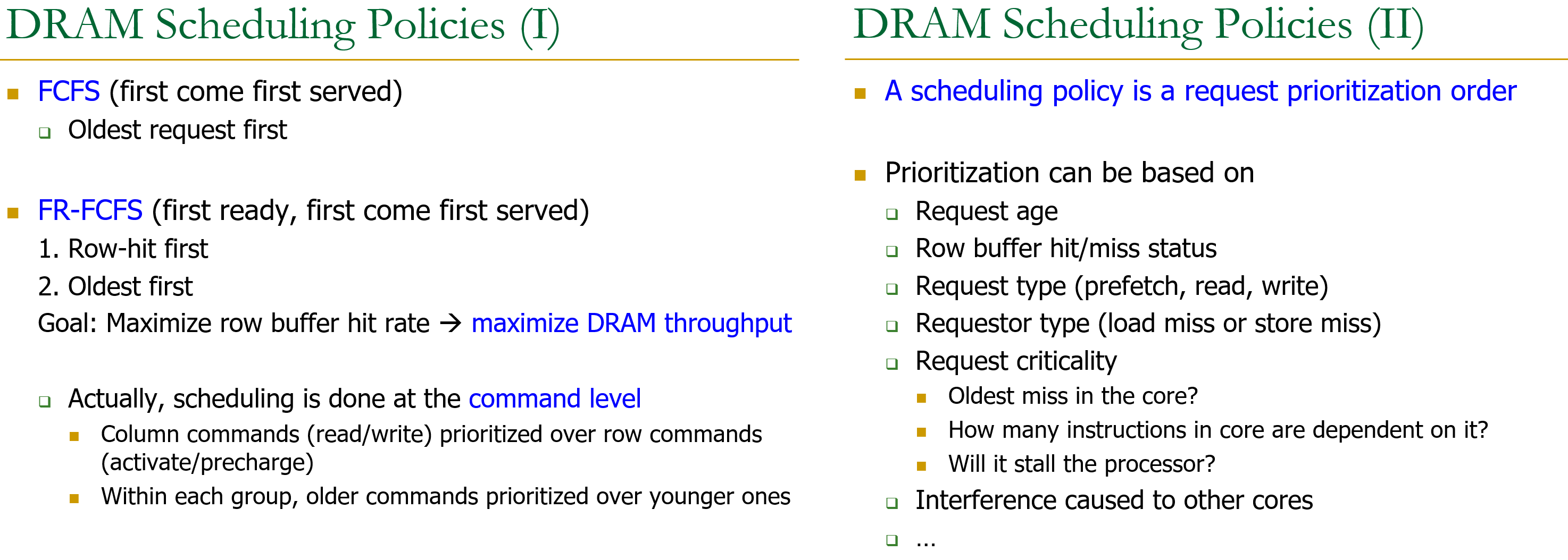
Row Buffer Management Policy determines if row buffer will be closed or remain opened after read/write access:

-
Activate opens the row and recharge the cell, we can read as long as open phase of activate is finished and then precharged only when recharge phase is over (precharge only when activate is completely finished)
-
DRAM simulator is very useful to provide abstraction when trying to add new features. Ramulator is one such simulator:

-
The DDR3 memory operates at high speeds, and the internal DLL helps to ensure that the data is read and written at the correct time. The DLL takes in the external clock signal and creates a new clock signal that is phase-aligned with the incoming data.
-
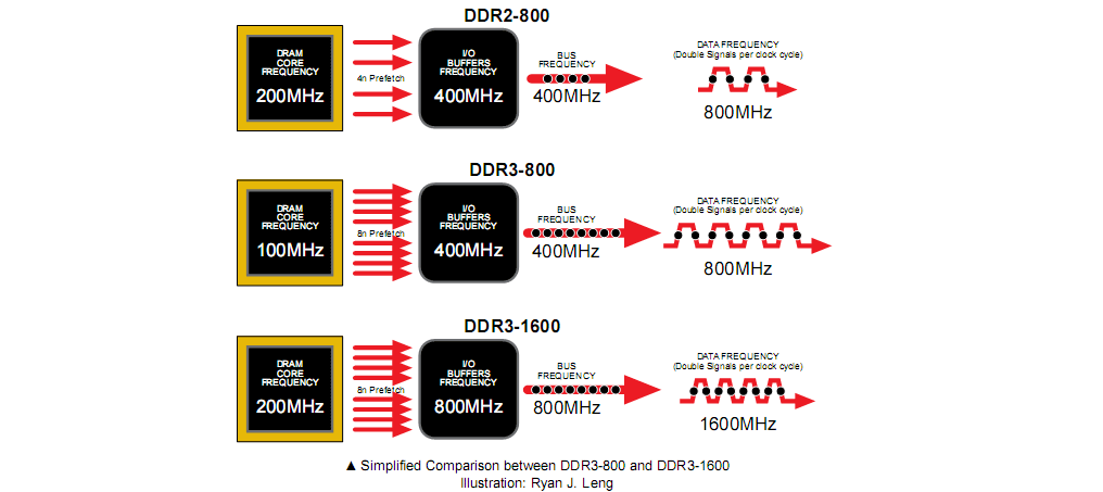
The the DRAM core frequency is low (100-200 MHz), but with prefetching high data throughput can be achieved:
-
You can use Micron DDR3 Simulation module to test the controller even without physical ddr3
-
ODDR2 is just used so that the internal clock can be directed to the output pin, this is the more likely use than doing DDR using ODDR2. dq_w is also connected to ODDR2 (with clk_90 and ~clk_90 since DQ is always 90 phase shifted when writing to RAM), multiple ODDR2 is instantiated using
generate -
OBUF is used to connect the internal pins to FPGA output pin
-
Output flow: OSERDES -> ODDR2 (output DDR buffer) -> ODELAY (DQS Centering) -> IOBUF (for inout) -> RAM
-
Input flow: RAM -> IOBUF (for inout) -> IDELAY (DQS Centering) -> IDDR2 (input DDR buffer) -> ISERDES
-
Low Speed: Use the clk (50MHz) and divide the frequency by 4 to generate a slow clock than can be shifted 180 degrees or 90 degrees. LOW SPEED IS USED TO TEST CONTROLLER BEFORE RUNNING IN HIGHER FREQUENCY
-
High Speed: Use PLL to generate 333.333 MHz from 50MHZ.(with 0,90,180,270 phase shift) . Then use DPLL to dynamically change phase shift for read operation
-
Slow Clock (controller clock = clk 50MHz)
- Detect the incoming DQS if its high or low, then from this detect the rising and falling edges of DQS.
- Since we now know the rising and falling edges, we can now detect the middle of DQS (neither rising nor falling) and this is where can sample the incoming DQ.
- The controller clock is 4x the DDR RAM clock to detect the 0, 90, 180, and 270. 90 and 270 degrees are needed in READ operation since this is the middle of DQS rising-falling edges. 0 and 180 degrees is for differential output.
- Not highspeed (slow clock) so no IOBUF to control DQS and DQ, just assignment statement to output. With highspeed (fast clock), IOBUF is used on DQ and DQS.
-
Fast Clock (controller clock = clk_serdes 83.333MHz).
clk_serdesis @83.333MHz which is 1/4 of DDR clockck. Read or write burst operation will take 1clk_serdesor 4ck, this means we can still maximize reading or writing even a slower controller clock by issuing a burst with having SERDES ratio of 8 (1 burst).-
READ OPERATION
- Generate 333MHz ck_90, ck_180, and ck_270 via PLL (from 50MHz main clock)
- posedge of ck_dynamic_90 is used to sample odd number DQ, posedge of ck_dynamic_270 (or negedge of ck_dynamic_90) is used to sample even number DQ. This is then sent to clk_270 domain using asyn_fifo. The output is
dq_r_q0(even burst) anddq_r_q1(odd burst). dq_r_q0anddq_r_q1is then both sent to its respective deserializer, the parallel output will then be arranged to form the whole 8 burst data.- ISERDES (deserializer, series to parallel) is used to convert the high-speed serial data to low speed parallel data which can be processed on lower clock frequency (50MHz main clock). Using only one ISERDES will be complicated since we will need to arrange the high speed serial data (from d0-d2-d4-d6 and d1-d3-d5-d7 to d0-d1-d2-d3-d4-d5-d6-d7) so we will use two separate SERDES and just arrange the low speed parallel data which is much easier.
// why need IOSERDES primitives ? // because you want a memory transaction rate (333MHz) much higher than the main clock frequency (50MHz) // but you don't want to require a very high main clock frequency (main clock is maintained to just 50MHz) // send a write of 8w (1 burst) bits to the memory controller, // which is similar to bundling multiple transactions into one wider one, // and the memory controller issues 8 writes of w bits to the memory, // where w is the data width of your memory interface. (w == DQ_BITWIDTH) // This literally means SERDES_RATIO=8 -
WRITE OPERATION
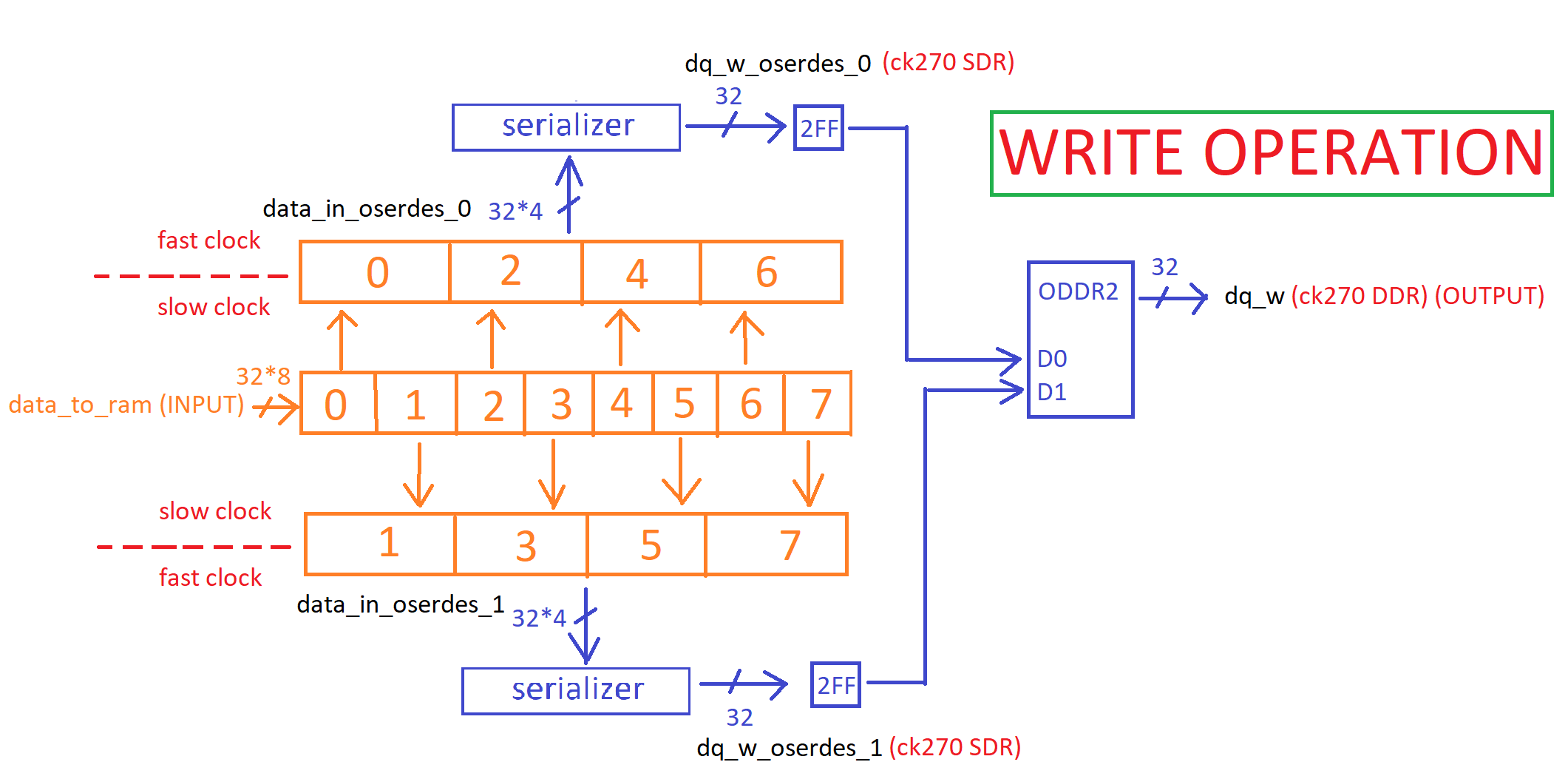
- OSERDES (serializer, parallel to series) is only SDR (Single-Data Rate) so unless the OSERDES is DDR, we will need two separate OSERDES. The output of these 2 OSERDES (
dq_w_d0anddq_w_d1) will be used by ODDR2 to form the double data rate output ofdq_w.
// There is need to use two separate OSERDES because ODDR2 expects its D0 and D1 inputs to be // presented to it at a DDR clock rate of 303MHz (D0 at posedge of 303MHz, D1 at negedge of 303MHz), // where 303MHz is the minimum DDR3 RAM working frequency. // However, one single SDR OSERDES alone could not fulfill this data rate requirement of ODDR2 (unless the OSERDES is DDR) // For example, a 8:1 DDR OSERDES which takes 8 inputs D0,D1,D2,D3,D4,D5,D6,D7 and output them serially // The values supplied by D0,D2,D4,D6 are clocked out on the rising edge // The values supplied by D1,D3,D5,D7 are clocked out on the falling edge // The solution is to create two 4:1 SDR OSERDES modules. // One of the 2 modules will take D0,D2,D4,D6 inputs and output them serially. You route its output to the D0 pin of the ODDR. // The other will output D1,D3,D5,D7 serially. You route its output to the D1 pin of the ODDR. - OSERDES (serializer, parallel to series) is only SDR (Single-Data Rate) so unless the OSERDES is DDR, we will need two separate OSERDES. The output of these 2 OSERDES (
-
IODELAY2 is not used "due to some internal hardware issues of Spartan 6". In read operation, "PLL dynamic phase shift is used in lieu of IODELAY2 primitive for phase shift alignment between READ DQS strobe and 'ck' signal".
- The first instance of IODELAY2 is used as input delay for read operation, delay the
dq_rby half clock period by default sockcan now sample the DQ at center of the data eye, instead of usingck_90andck_270to sample the DQ. The delay can be adjusted for MPR read calibration method. - The second instance of IODELAY is used also as input delay but for write operation, delay the
dq_woutput from ODDR2 (clocked byck) by 90 from DQS instead of usingck_90to clock ODDR2. This delay is for write calibration levelling.
// the IODELAY2 primitives for DQ bits could not be shared between read and write operations // because if they are to be shared, they would be some combinational logic to select between // read and write operations which is not helpful at all for read operations. // Note that for read pipeline, IDELAY is used before ISERDES, which means any extra logic for input of // IDELAY will slow things down significantly until the read operations might fail to calibrate delay- MPR Read Calibration will then be used to align the DQS (phase shifted initially by zero) to ck via the IODELAY. Aligning the DQS will also align DQ (already shifted by 90).
- The first instance of IODELAY2 is used as input delay for read operation, delay the
-
Observation: On read operation, we are still using
ckto sample the dq_r, and we are not depending on DQ_S -
data_read_is_ongoing(clk_serdes) -> ck -> dqs_iobuf_en
data_read_is_ongoing(clk_serdes) -> ck270 -> dq_iobuf_en- For non-x16, tri-state controller is
data_read_is_ongoingbut for x16 itsdqs_iobuf_en.
Why dq_iobuf_en at ck270 domain? hypothesis: dq_r is sampled at ck270 and ck90, thus dq_r is on ck270 dq_w must also be on ck270 since DQ is shifted by 90 from DQS THUS dq_iobuf_en is also on ck270 - For non-x16, tri-state controller is
-
It is possible to do all 8 refresh commands inside one tREFI cycles then postpone refresh commands for 9*tREFI. tREFI is the "average" interval between REFRESH commands.
-
reset (input, clk domain) is synced to ck_270 domain as reset input to IPs like IOSERDES.
-
Controller FSM (clk_serdes, 83.3333MHz) sends
main_state,dram_command_bits,r_address, andr_bank_addressto asyn_fifo to ck_180 (333MHz) then to external pins. -
FIFO can be used for queueing commands BUT IS NOT USED ON THIS DESIGN. Full-rate DRAM commands transaction is possible with the usage of either (an OSERDES with a serialization factor of 2) or (2 words ck/2 in, ck out FIFO). You can stuff multiple user request commands where permitted in between command execution inside DRAM. One example would be where other banks may be activated while a write command was just sent.
-
On this design, the SERDES enable multiple read and write (1 burst, 1 command for 1 clk_serdes) BUT IT CANNOT DO MULTIPLE COMMANDS AT ONCE (there is no command FIFO queue so at clk_serdes 83.333MHz, there can only be 1 command per 1 clk_serdes or 4 ck cycle of 333MHz)
-
Only at the first cycle of each FSM state are cmd sent, the rest are NOPs.

-
Uses conventional FSM. 1 state 1 command and will stay there until the time parameter is over (so interleaving is impossible since you had to finish the time delay allotted for every command and cannot interleave commands like read then activate another bank while on read latency).
-
Ddr initialization (200us and 500us) requires long bitwidth counter and thus larger comparison hardware so we can divide the counter by two for less logic.
-
FSM flow for initialization: reset-> reset_finish -> init_clock_enable -> MRS2 -> MRS3 (no MPR yet set since ZQCL needs to finish first) -> MRS3_TO_MRS1 -> MRS1 -> MRS0 -> ZQ_CALIBRATION (set MPR enable) -> IDLE -> STATE_PRECHARGE -> MRS3 (again but MPR is now set for read calibration) -> READ_AP (sync on delay chain) -> READ_AP_ACTUAL (issue read cmd and wait for latency) -> Read_data (after 1burst read, set MPR disable) -> MRS3-> wait_after_MPR -> IDLE
-
AL (additive latency) can be used somehow to save a few cycles when you ACTIVATE multiple banks interleaved. This source explains well and have examples on bank interleaving.
-
"After enabling the clock outputs (ck) during initialization, the DLL in the RAM needs to "lock" to the clock signal. A DLL reset "unlocks" the DLL, so that it can lock again to the current clock speed. The DLL is then used to generate DQS. For read commands, the DRAM drives DQ and DQS pins, and uses the DLL to maintain a 90 degrees phase shift between DQ and DQS."
-
"READ/WRITE normally go first and refreshes are done while no READ/WRITE are pending, unless there is a danger that the queue underflows, in which case it becomes a high-priority request and READ/WRITE have to wait. So, in summary, it is to overcome the performance penalty due to refresh lockout at the higher densities"
-
Refresh operation flow: IDLE -> Precharge -> Refresh (decrease refresh queue) -> IDLE -> (repeat)
-
Write operation flow: IDLE (get bank addr, activate) -> Activate (get bank and col addr, write) -> write_ap(get col addr, burst+1, write) -> write_data (get col addr, burst+1, write) -> write_ap (get col_addr, burst+1, write) -> write_data (get col addr, finish autoprecharge) -> IDLE
-
Read operation flow: IDLE (get bank addr, activate) -> Activate (get bank and col addr, read) -> read_ap (get col adress) -> read_ap_actual (get col addr, read) -> read_data (get col addr, burst+1, read) -> read_ap_actual (get col addr, read) -> read_data (get col addr) -> IDLE
-
FSM controls
data_read_is_ongoingwhich specify direction of DQ. The PHY interface continuously reads fromdq_rand generates outputdata_from_ram, and also continuously writes from inputdata_to_ramtodq_wregardless of what FSM state. Thedata_read_is_ongoingis the one who decides if the DQ will be owned by read (dq_r) or write (dq_w). -
"We can just send a spree of refresh commands, then wait some time (9x the nominal period 9*tREFI), then send another spree because that works out to about the nominal period and the refresh scheduler in the DRAM will do the rest".
-
-
Due to PCB trace layout and high-speed DDR signal transmission, there is no alignment to any generic clock signal that we can depend upon, especially when data is coming back from the SDRAM chip. Thus, we could only depend upon incoming
DQSsignal to sample 'DQ' signal -
In differntial signals (DQS-DQS_n and CK-CK_n), you must not use inverter to generate the differential signal or else there will be time skew between the positive and negative signal. SO, generate the differential signal separately without relying in inverter logic
-
DQ, DQS, DQS_n = IOBUF
-
CK and CK_n = OBUF
- Use DDR3-1600 with 800MHz clock. Since its impossible to get the logic to pass timing at that speed, use 200MHz. Data is 16-bit thus to reach full speed at 200MHz (5ns clk), we need to transfer 128-bits (16 x 2DDR x 800MHz/200MHz = 16x2x4 = 128) per 5ns and issue 4 commands (800MHz/200MHz = 4) per 5ns.
- On "Artix-7 FPGAs Data Sheet: DC and AC Switching Characteristics" shows possible DDR3 PHY rate
- Memory and DRAM Basics Series (Onur Mutlu Lectures)
- DRAM Basics in 7-part Series (Computer Science)
- DDR DRAM Basics (VLSIGuru Training Institute)
- SoftMC and RowHammer Series (Onur Mutlu Lectures)
- Memory Controllers (Onur Mutlu Lectures)
- DDR4 Timings Explained Manually Series (Actually Hardcore Overclocking)
- Transprecision-aware DDR Controller with PHY (oprecomp)
- DRAM Basic Commands
- SDRAM as simple state machine (SERIES)
- DDR4 SDRAM - Initialization, Training and Calibration
- DDR operation and timing parameters
- DDR Read and Write Operation
- DDR3 Write Leveling and Read Leveling
- Why need write and read leveling? (SERIES)
- More on write and read leveling
- Why use DQS for read/write?
- ODT and ZQ Calibration (SERIES)


