[go: up one dir, main page]

Skip to main content
U.S. flag

An official website of the United States government

Official websites use .gov
A .gov website belongs to an official government organization in the United States.

Secure .gov websites use HTTPS
A lock ( ) or https:// means you’ve safely connected to the .gov website. Share sensitive information only on official, secure websites.

Nanostructure Fabrication and Measurement Group

Creates positive feedback between making and measuring nanostructures, to cultivate new capabilities for nanotechnology and nanomanufacturing.

The Nanostructure Fabrication and Measurement Group has established and is exploring a virtuous cycle of making and measuring nanostructures, with the goal of developing approaches that are broadly deployable in research and manufacturing. By creating and advancing methods to measure nanofabrication processes, we improve understanding and quality of nanostructure fabrication. We then apply accurate and precise nanostructures to make metrology methods as good as in the lab, as fast as in the fab. This positive feedback loop improves the theory and practice of fabrication processes, supports the development of novel device technologies, and enables new measurements at the nanometer scale. In this way, the Division creates new capabilities of accuracy and efficiency for nanotechnology and nanomanufacturing. Stakeholder needs inform a current focus on three application areas of production of photonic, electronic, and fluidic devices, innovation of microscopy methods, standards, and calibrations, and characterization of nanoparticle products and nanoplastic byproducts.

News and Updates

Projects and Programs

Atomic-force microscopy

Ongoing
Atomic-force microscopy enables subnanometer imaging resolution, to extract geometric parameters of reference structures that advance measurement science, and to quantify the accuracy of device design and fabrication for stakeholders. We are advancing two primary atomic-force microscopy systems

Biomolecular assembly

Ongoing
The integration of new materials or components into the design and production of diverse nanotechnologies, ranging from electronic devices to therapeutic particles, requires a quantitative understanding of process–structure–property relationships, as well as interactions with other entities in the

Electron-beam lithography

Ongoing
Electron-beam lithography allows fine control of nanostructure features that form the basis of diverse device technologies. Lateral resolution of 10 nm, placement accuracy of 1 nm, and patterning fields of 1 mm are all possible. However, achieving these performance metrics depends on many

Electron-Solid Interactions

Ongoing
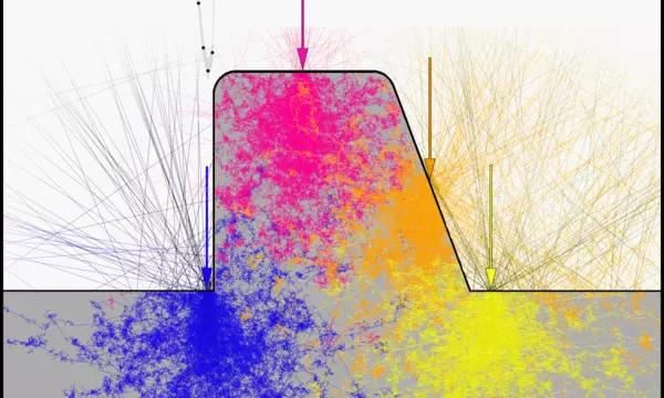
A measuring instrument produces a signal that depends upon the value of the measurand. The value and its uncertainty are inferred from the signal by using a model of their relationship. Erroneous models lead to erroneous inference. The accuracy of SEM (scanning electron microscopy) is limited by

Publications

Revealing thermodynamics of DNA origami folding via affine transformations

Author(s)
Jacob M. Majikes, Paul N. Patrone, Daniel R. Schiffels, Michael P. Zwolak, Anthony J. Kearsley, Samuel P. Forry, James A. Liddle
Structural DNA nanotechnology, as exemplified by DNA origami, has enabled the design and construction of molecularly precise objects for a myriad of

Awards

2010 APS Fellow - John Kasianowicz

For his pioneering contributions to the field of biophysics including the detection, identification, characterization and quantification of

Contacts

Group Leader

General Information