[go: up one dir, main page]

Next Issue
Volume 7, March
Previous Issue
Volume 6, September


Photonics, Volume 6, Issue 4 (December 2019) – 28 articles

Cover Story (view full-size image): 
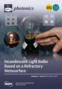
The prototype of an incandescent light bulb with a refractory metasurface filament is demonstrated using the nanoimprint method. An array of microcavity is fabricated on a tantalum (Ta) substrate and implemented into the bulb. It enhances incandescence around the resonant wavelength of the cavity in thermal radiation. In addition, a refractory plasmonic metasurface composed of hafnium nitride (HfN) meta-atoms emits narrow-band thermal radiation at a wavelength of 4.1 micrometers and suppresses longer wavelength emission to the peak. It is predicted to enhance power efficiency by four times compared to a bare surface in theory. The implementation of refractory plasmonic metasurface so-called “metafilament” into a light bulb paves the way for the realization of a full-spectral eco-lamp in future.View this paper.
  • Issues are regarded as officially published after their release is announced to the table of contents alert mailing list.
  • You may sign up for e-mail alerts to receive table of contents of newly released issues.
  • PDF is the official format for papers published in both, html and pdf forms. To view the papers in pdf format, click on the "PDF Full-text" link, and use the free Adobe Reader to open them.
Order results
Result details
Section
Select all
Export citation of selected articles as:
8 pages, 2473 KiB  
Article
Image Encryption System Based on a Nonlinear Joint Transform Correlator for the Simultaneous Authentication of Two Users
by Juan M. Vilardy O., María S. Millán and Elisabet Pérez-Cabré
Photonics 2019, 6(4), 128; https://doi.org/10.3390/photonics6040128 - 14 Dec 2019
Cited by 5 | Viewed by 2779
Abstract
We propose a new encryption system based on a nonlinear joint transform correlator (JTC) using the information of two biometrics (one digital fingerprint for each user) as security keys of the encryption system. In order to perform the decryption and authentication in a [...] Read more.
We propose a new encryption system based on a nonlinear joint transform correlator (JTC) using the information of two biometrics (one digital fingerprint for each user) as security keys of the encryption system. In order to perform the decryption and authentication in a proper way, it is necessary to have the two digital fingerprints from the respective users whose simultaneous authentication is pursued. The proposed security system is developed in the Fourier domain. The nonlinearity of the JTC along with the five security keys given by the three random phase masks and the two digital fingerprints of the two users allow an increase of the system security against brute force and plaintext attacks. The feasibility and validity of this proposal is demonstrated using digital fingerprints as biometrics in numerical experiments. Full article
Show Figures

Figure 1

Figure 1
<p>(<b>a</b>) The scheme of the optical setup composed of an encryption system based on a nonlinear JTC architecture (part I) and a decryption system based on a 4<span class="html-italic">f</span>-processor (part II). Distributions contained in the input plane of the (<b>b</b>) encryption system, and (<b>c</b>) decryption system.</p>
Full article ">Figure 2
<p>(<b>a</b>) Original image to encrypt <math display="inline"><semantics> <mrow> <mi>f</mi> <mo>(</mo> <mi>x</mi> <mo>,</mo> <mi>y</mi> <mo>)</mo> </mrow> </semantics></math>. (<b>b</b>) Random code image <math display="inline"><semantics> <mrow> <mi>s</mi> <mo>(</mo> <mi>x</mi> <mo>,</mo> <mi>y</mi> <mo>)</mo> </mrow> </semantics></math> of the random phase mask (RPM) <math display="inline"><semantics> <mrow> <mi>r</mi> <mo>(</mo> <mi>x</mi> <mo>,</mo> <mi>y</mi> <mo>)</mo> </mrow> </semantics></math>. Images of the digital fingerprints of the two users: (<b>c</b>) first user <math display="inline"><semantics> <mrow> <msub> <mi>p</mi> <mn>1</mn> </msub> <mrow> <mo>(</mo> <mi>x</mi> <mo>,</mo> <mi>y</mi> <mo>)</mo> </mrow> </mrow> </semantics></math> and (<b>d</b>) second user <math display="inline"><semantics> <mrow> <msub> <mi>p</mi> <mn>2</mn> </msub> <mrow> <mo>(</mo> <mi>x</mi> <mo>,</mo> <mi>y</mi> <mo>)</mo> </mrow> </mrow> </semantics></math>. (<b>e</b>) Encrypted image <math display="inline"><semantics> <mrow> <mi>E</mi> <mo>(</mo> <mi>u</mi> <mo>,</mo> <mi>v</mi> <mo>)</mo> </mrow> </semantics></math>. (<b>f</b>) Decrypted image <math display="inline"><semantics> <mrow> <mover accent="true"> <mi>f</mi> <mo stretchy="false">^</mo> </mover> <mrow> <mo>(</mo> <mi>x</mi> <mo>,</mo> <mi>y</mi> <mo>)</mo> </mrow> </mrow> </semantics></math> using the correct five security keys (<math display="inline"><semantics> <mrow> <mi>r</mi> <mo>(</mo> <mi>x</mi> <mo>,</mo> <mi>y</mi> <mo>)</mo> </mrow> </semantics></math>, <math display="inline"><semantics> <mrow> <msub> <mi>k</mi> <mn>1</mn> </msub> <mrow> <mo>(</mo> <mi>x</mi> <mo>,</mo> <mi>y</mi> <mo>)</mo> </mrow> </mrow> </semantics></math>, <math display="inline"><semantics> <mrow> <msub> <mi>k</mi> <mn>2</mn> </msub> <mrow> <mo>(</mo> <mi>x</mi> <mo>,</mo> <mi>y</mi> <mo>)</mo> </mrow> </mrow> </semantics></math>, <math display="inline"><semantics> <mrow> <msub> <mi>p</mi> <mn>1</mn> </msub> <mrow> <mo>(</mo> <mi>x</mi> <mo>,</mo> <mi>y</mi> <mo>)</mo> </mrow> </mrow> </semantics></math> and <math display="inline"><semantics> <mrow> <msub> <mi>p</mi> <mn>2</mn> </msub> <mrow> <mo>(</mo> <mi>x</mi> <mo>,</mo> <mi>y</mi> <mo>)</mo> </mrow> </mrow> </semantics></math>). Decrypted images for the following wrong security keys: (<b>g</b>) the image of the digital fingerprint of the first user <math display="inline"><semantics> <mrow> <msub> <mi>p</mi> <mn>1</mn> </msub> <mrow> <mo>(</mo> <mi>x</mi> <mo>,</mo> <mi>y</mi> <mo>)</mo> </mrow> </mrow> </semantics></math> and (<b>h</b>) the RPM <math display="inline"><semantics> <mrow> <msub> <mi>k</mi> <mn>2</mn> </msub> <mrow> <mo>(</mo> <mi>x</mi> <mo>,</mo> <mi>y</mi> <mo>)</mo> </mrow> </mrow> </semantics></math>.</p>
Full article ">
10 pages, 5481 KiB  
Article
The Effect of Thickness on the Properties of Laser-Deposited NiBSi-WC Coating on a Cu-Cr-Zr Substrate
by Yury Korobov, Yulia Khudorozhkova, Holger Hillig, Alexander Vopneruk, Aleksandr Kotelnikov, Sergey Burov, Prabu Balu, Alexey Makarov and Alexey Chernov
Photonics 2019, 6(4), 127; https://doi.org/10.3390/photonics6040127 - 13 Dec 2019
Cited by 3 | Viewed by 3145
Abstract
Ni/60WC coatings on copper substrate were placed via laser deposition (LD). A structural study was conducted using electron microscopy and a microhardness evaluation. Two body abrasive wear tests were conducted with a pin-on-plate reciprocating technique. A tool steel X12MF GOST 5960 (C-Cr-Mo-V 1.6-12-0.5-0.2) [...] Read more.
Ni/60WC coatings on copper substrate were placed via laser deposition (LD). A structural study was conducted using electron microscopy and a microhardness evaluation. Two body abrasive wear tests were conducted with a pin-on-plate reciprocating technique. A tool steel X12MF GOST 5960 (C-Cr-Mo-V 1.6-12-0.5-0.2) with a hardness of 63 HRC was used as a counterpart. The following results were obtained: Precipitation of the secondary carbides takes place in the thicker layers. Their hardness is lower than that of the primary carbides in the deposition (2425 HV vs. 2757 HV) because they mix with the matrix material. In the thin layers, precipitation is restricted due to a higher cooling rate. For both LD coatings, the carbide’s hardness increases compared to the initial mono-tungsten carbide (WC)-containing powder (2756 HV vs. 2200 HV). Such a high level of microhardness reflects the combined influence of a low level of thermal destruction of carbides during laser deposition and the formation of a boride-strengthening phase from the matrix powder. The thicker layer showed a higher wear resistance; weight loss was 20% lower. The changes in the thickness of the laser deposited Ni-WC coating altered its structure and wear resistance. Full article
(This article belongs to the Special Issue Advanced Optical Materials and Devices)
Show Figures

Figure 1

Figure 1
<p>View of the samples as deposited: (<b>a</b>) Laser deposition (LD)-thin; (<b>b</b>) LD-thick.</p>
Full article ">Figure 2
<p>SEM image: Carbide particles surrounded by a matrix in LD coating: (<b>a</b>) LD-thin; (<b>b</b>) LD-thick.</p>
Full article ">Figure 3
<p>Elemental mapping analysis in the characteristic spectra: (<b>a</b>) Ni; (<b>b</b>) W; (<b>c</b>) B. The image corresponds to LD-thin coating, <a href="#photonics-06-00127-f002" class="html-fig">Figure 2</a>a.</p>
Full article ">Figure 4
<p>Elemental mapping analysis in the characteristic spectra: (<b>a</b>) Ni; (<b>b</b>) W; (<b>c</b>) B. The image corresponds to LD-thick coating, <a href="#photonics-06-00127-f002" class="html-fig">Figure 2</a>b.</p>
Full article ">Figure 5
<p>A view of crack propagation in carbide particle of LD-thick layer.</p>
Full article ">Figure 6
<p>The distribution of elements in the cross section of the coating from the surface to the substrate, (<b>a</b>) LD-thin; (<b>b</b>) LD-thick.</p>
Full article ">Figure 7
<p>Wear surface: (<b>a</b>) Thick coating; (<b>b</b>) thin coating. (<b>1</b>) Matrix; (<b>2</b>) supporting sections of carbides; (<b>3</b>) transitional section.</p>
Full article ">
13 pages, 12141 KiB  
Article
An Optoelectronic Targeting System for Measuring the Distribution of Projectile Motion Based on the Subdivision of a Light Screen
by Wenbo Chu, Bin Zhang, Baowei Liu, Zhiguo Gui and Donge Zhao
Photonics 2019, 6(4), 126; https://doi.org/10.3390/photonics6040126 - 12 Dec 2019
Cited by 12 | Viewed by 2812
Abstract
This paper proposes a cost-effective, compact, noncontacting optoelectronic targeting system for measuring the distribution of projectile motion. The major elements of this system include a light emitting diode (LED) array, photodiode detecting array, double-layered aperture arrays, adaptive threshold circuit, and date acquisition. Through [...] Read more.
This paper proposes a cost-effective, compact, noncontacting optoelectronic targeting system for measuring the distribution of projectile motion. The major elements of this system include a light emitting diode (LED) array, photodiode detecting array, double-layered aperture arrays, adaptive threshold circuit, and date acquisition. Through cooperating with double-layered aperture arrays, the system effectively reduces the radiation width of the light source to the photodiode detecting surface, and filters out the influence of incident light from the adjacent apertures on both sides above each photodiode to the corresponding photodiode detecting surface. It realizes that the response of the photodiode array corresponds to the coordinates of the light screen one by one. Through the sensitivity analysis of the light screen of the system, the system detecting threshold when the projectile passes through the light screen is calculated, and the corresponding adaptive threshold circuit is designed to prevent misjudgment when the system works. The measuring error of the system can reach ±2 mm by experimental verification. Compared with other projectile’s distribution measuring systems, the proposed system has the advantages of having high precision, convenient debugging, is nondestructive, and is a noncontact system. Full article
(This article belongs to the Section Lasers, Light Sources and Sensors)
Show Figures

Figure 1

Figure 1
<p>The principle components for coordinate measurement of projectiles.</p>
Full article ">Figure 2
<p>Mathematical model of single-layered aperture. Note: PD = photodiode; LED = light emitting diode.</p>
Full article ">Figure 3
<p>Mathematical model of double-layered apertures.</p>
Full article ">Figure 4
<p>Schematic diagram for maximum error.</p>
Full article ">Figure 5
<p>Optical simulation model of the system.</p>
Full article ">Figure 6
<p>Light intensity distribution curve of the PD detecting array before and after adding the aperture array.</p>
Full article ">Figure 7
<p>Simulation model for detecting sensitivity in the light screen.</p>
Full article ">Figure 8
<p>Detecting sensitivity curve of the single PD detector at positions 100 mm, 300 mm, 600 mm, 900 mm, 1200 mm, and 1400 mm from the LED array.</p>
Full article ">Figure 9
<p>Sensitivity distribution of an effective light screen.</p>
Full article ">Figure 10
<p>Design flow of the adaptive threshold circuit.</p>
Full article ">Figure 11
<p>Circuit for generating over-target pulse signals.</p>
Full article ">Figure 12
<p>Adaptive threshold circuit.</p>
Full article ">Figure 13
<p>Digital pulse signal and analog signal of the projectile’s over-target display.</p>
Full article ">Figure 14
<p>Acquisition daughter board of system.</p>
Full article ">Figure 15
<p>Identified method for the projectile’s coordinate.</p>
Full article ">Figure 16
<p>Layout of the measuring site.</p>
Full article ">
14 pages, 791 KiB  
Article
Synchronization of Mutually Delay-Coupled Quantum Cascade Lasers with Distinct Pump Strengths
by Thomas Erneux and Daan Lenstra
Photonics 2019, 6(4), 125; https://doi.org/10.3390/photonics6040125 - 10 Dec 2019
Cited by 14 | Viewed by 2966
Abstract
The rate equations for two delay-coupled quantum cascade lasers are investigated analytically in the limit of weak coupling and small frequency detuning. We mathematically derive two coupled Adler delay differential equations for the phases of the two electrical fields and show that these [...] Read more.
The rate equations for two delay-coupled quantum cascade lasers are investigated analytically in the limit of weak coupling and small frequency detuning. We mathematically derive two coupled Adler delay differential equations for the phases of the two electrical fields and show that these equations are no longer valid if the ratio of the two pump parameters is below a critical power of the coupling constant. We analyze this particular case and derive new equations for a single optically injected laser where the delay is no longer present in the arguments of the dependent variables. Our analysis is motivated by the observations of Bogris et al. (IEEE J. Sel. Top. Quant. El. 23, 1500107 (2017)), who found better sensing performance using two coupled quantum cascade lasers when one laser was operating close to the threshold. Full article
(This article belongs to the Special Issue Semiconductor Laser Dynamics: Fundamentals and Applications)
Show Figures

Figure 1

Figure 1
<p>Frequency-locked states in the case of zero delay. <math display="inline"><semantics> <mrow> <mi>σ</mi> <mo>=</mo> <msub> <mo>Φ</mo> <mn>2</mn> </msub> <mo>−</mo> <msub> <mo>Φ</mo> <mn>1</mn> </msub> </mrow> </semantics></math> is shown as a function of <math display="inline"><semantics> <mo>Δ</mo> </semantics></math> (<math display="inline"><semantics> <mrow> <mo>−</mo> <mi>π</mi> <mo>&lt;</mo> <mo>Φ</mo> <mo>&lt;</mo> <mi>π</mi> <mo>)</mo> <mo>.</mo> <mspace width="4pt"/> </mrow> </semantics></math> Full and broken lines correspond to stable and unstable branches. <math display="inline"><semantics> <mrow> <msub> <mi>θ</mi> <mn>0</mn> </msub> <mo>=</mo> <mi>π</mi> <mo>/</mo> <mn>4</mn> <mo>,</mo> </mrow> </semantics></math> <math display="inline"><semantics> <mrow> <mi>ε</mi> <mo>=</mo> <mn>0.02</mn> <mo>,</mo> </mrow> </semantics></math> <math display="inline"><semantics> <mrow> <mi>α</mi> <mo>=</mo> <mn>1</mn> <mo>,</mo> </mrow> </semantics></math> <math display="inline"><semantics> <mrow> <msub> <mi>P</mi> <mn>1</mn> </msub> <mo>=</mo> <mn>1</mn> <mo>,</mo> </mrow> </semantics></math> and the value of <math display="inline"><semantics> <msub> <mi>P</mi> <mn>2</mn> </msub> </semantics></math> is indicated in the figure.</p>
Full article ">Figure 2
<p>Compound laser mode (CLM) frequencies <math display="inline"><semantics> <mrow> <mi>ω</mi> <mi>τ</mi> </mrow> </semantics></math> and phase difference <math display="inline"><semantics> <mi>σ</mi> </semantics></math> for the case <math display="inline"><semantics> <mrow> <msub> <mi>P</mi> <mn>1</mn> </msub> <mo>=</mo> <msub> <mi>P</mi> <mn>2</mn> </msub> <mo>.</mo> <mspace width="4pt"/> </mrow> </semantics></math> They are determined from the parametric solution Equations (<a href="#FD23-photonics-06-00125" class="html-disp-formula">23</a>) and (<a href="#FD24-photonics-06-00125" class="html-disp-formula">24</a>). The fixed parameters are <math display="inline"><semantics> <mrow> <msub> <mi>θ</mi> <mn>0</mn> </msub> <mo>=</mo> <mi>π</mi> <mo>/</mo> <mn>4</mn> <mo>,</mo> </mrow> </semantics></math> <math display="inline"><semantics> <mrow> <mi>τ</mi> <mo>=</mo> <mn>13.33</mn> <mo>,</mo> </mrow> </semantics></math> <math display="inline"><semantics> <mrow> <mi>ε</mi> <mo>=</mo> <mn>0.021</mn> <mo>,</mo> </mrow> </semantics></math> and <math display="inline"><semantics> <mrow> <mi>α</mi> <mo>=</mo> <mn>1</mn> <mo>.</mo> </mrow> </semantics></math> The extrema of <math display="inline"><semantics> <mrow> <mi>ω</mi> <mi>τ</mi> </mrow> </semantics></math> are <math display="inline"><semantics> <mrow> <mi>ω</mi> <msub> <mi>τ</mi> <mo>−</mo> </msub> <mo>=</mo> <mo>−</mo> <mn>0.32</mn> </mrow> </semantics></math> and <math display="inline"><semantics> <mrow> <mi>ω</mi> <msub> <mi>τ</mi> <mo>+</mo> </msub> <mo>=</mo> <mn>0.22</mn> <mo>.</mo> <mspace width="4pt"/> </mrow> </semantics></math> The extrema of <math display="inline"><semantics> <mrow> <mo>Δ</mo> <mi>τ</mi> </mrow> </semantics></math> are the limit points <math display="inline"><semantics> <mrow> <mo>Δ</mo> <mi>τ</mi> <mo>=</mo> <mo>±</mo> <mo>Δ</mo> <msub> <mi>τ</mi> <mrow> <mi>L</mi> <mi>P</mi> </mrow> </msub> <mo>=</mo> <mo>±</mo> <mn>0.58</mn> <mo>.</mo> </mrow> </semantics></math> The interval <math display="inline"><semantics> <mrow> <mo>[</mo> <mo>−</mo> <mo>Δ</mo> <msub> <mi>τ</mi> <mrow> <mi>L</mi> <mi>P</mi> </mrow> </msub> <mo>,</mo> <mo>Δ</mo> <msub> <mi>τ</mi> <mrow> <mi>L</mi> <mi>P</mi> </mrow> </msub> <mo>]</mo> </mrow> </semantics></math> is the locking range, i.e., the detuning range where the lasers lock their frequencies.</p>
Full article ">Figure 3
<p>CLM frequencies for the case <math display="inline"><semantics> <mrow> <msub> <mi>P</mi> <mn>1</mn> </msub> <mo>=</mo> <msub> <mi>P</mi> <mn>2</mn> </msub> </mrow> </semantics></math> and for different values of <math display="inline"><semantics> <mrow> <msub> <mi>θ</mi> <mn>0</mn> </msub> <mspace width="4pt"/> </mrow> </semantics></math>(indicated in the figure). The fixed parameters are <math display="inline"><semantics> <mrow> <mi>τ</mi> <mo>=</mo> <mn>13.33</mn> <mo>,</mo> </mrow> </semantics></math> <math display="inline"><semantics> <mrow> <mi>ε</mi> <mo>=</mo> <mn>0.021</mn> <mo>,</mo> </mrow> </semantics></math> and <math display="inline"><semantics> <mrow> <mi>α</mi> <mo>=</mo> <mn>1</mn> <mo>.</mo> </mrow> </semantics></math> As we decrease <math display="inline"><semantics> <msub> <mi>θ</mi> <mn>0</mn> </msub> </semantics></math> from <math display="inline"><semantics> <mrow> <mi>π</mi> <mo>/</mo> <mn>2</mn> <mo>,</mo> </mrow> </semantics></math> the double orbits progressively change into a single orbit.</p>
Full article ">Figure 4
<p>The limit point <math display="inline"><semantics> <mrow> <mo>Δ</mo> <msub> <mi>τ</mi> <mrow> <mi>L</mi> <mi>P</mi> </mrow> </msub> <mo>&gt;</mo> <mn>0</mn> </mrow> </semantics></math> is shown as a function of <math display="inline"><semantics> <mrow> <msub> <mi>θ</mi> <mn>0</mn> </msub> <mo>.</mo> <mspace width="4pt"/> </mrow> </semantics></math> The maximum appears at <math display="inline"><semantics> <mrow> <msub> <mi>θ</mi> <mn>0</mn> </msub> <mo>=</mo> <mn>0</mn> </mrow> </semantics></math> and <math display="inline"><semantics> <mi>π</mi> </semantics></math> and is given by <math display="inline"><semantics> <mrow> <mo>Δ</mo> <msub> <mi>τ</mi> <mrow> <mi>L</mi> <mi>P</mi> </mrow> </msub> <mo>=</mo> <mi>ε</mi> <mi>τ</mi> <msqrt> <mrow> <mn>1</mn> <mo>+</mo> <msup> <mi>α</mi> <mn>2</mn> </msup> <mo>.</mo> </mrow> </msqrt> </mrow> </semantics></math></p>
Full article ">Figure 5
<p>CLMs for small values of <math display="inline"><semantics> <mrow> <msub> <mi>P</mi> <mn>2</mn> </msub> <mo>/</mo> <msub> <mi>P</mi> <mn>1</mn> </msub> <mo>.</mo> </mrow> </semantics></math> <math display="inline"><semantics> <mrow> <msub> <mi>P</mi> <mn>1</mn> </msub> <mo>=</mo> <mn>1</mn> </mrow> </semantics></math>, and the value of <math display="inline"><semantics> <msub> <mi>P</mi> <mn>2</mn> </msub> </semantics></math> is indicated in the figure. The fixed parameters are <math display="inline"><semantics> <mrow> <mi>τ</mi> <mo>=</mo> <mn>13.33</mn> <mo>,</mo> </mrow> </semantics></math> <math display="inline"><semantics> <mrow> <mi>ε</mi> <mo>=</mo> <mn>0.021</mn> <mo>,</mo> </mrow> </semantics></math> <math display="inline"><semantics> <mrow> <msub> <mi>θ</mi> <mn>0</mn> </msub> <mo>=</mo> <mi>π</mi> <mo>/</mo> <mn>4</mn> <mo>,</mo> </mrow> </semantics></math> and <math display="inline"><semantics> <mrow> <mi>α</mi> <mo>=</mo> <mn>1</mn> <mo>.</mo> </mrow> </semantics></math></p>
Full article ">Figure 6
<p>The extrema <math display="inline"><semantics> <mrow> <mi>ω</mi> <msub> <mi>τ</mi> <mo>±</mo> </msub> </mrow> </semantics></math> as functions of <math display="inline"><semantics> <mrow> <mi>x</mi> <mo>=</mo> <msub> <mi>P</mi> <mn>2</mn> </msub> <mo>/</mo> <msub> <mi>P</mi> <mn>1</mn> </msub> </mrow> </semantics></math> are obtained by solving the quadratic Equation (<a href="#FD29-photonics-06-00125" class="html-disp-formula">29</a>). Their approximations as <math display="inline"><semantics> <mrow> <mi>x</mi> <mo>→</mo> <mn>0</mn> </mrow> </semantics></math> are given by Equation (<a href="#FD30-photonics-06-00125" class="html-disp-formula">30</a>) (dotted red lines). The fixed parameters are <math display="inline"><semantics> <mrow> <mi>τ</mi> <mo>=</mo> <mn>13.33</mn> <mo>,</mo> </mrow> </semantics></math> <math display="inline"><semantics> <mrow> <mi>ε</mi> <mo>=</mo> <mn>0.021</mn> <mo>,</mo> </mrow> </semantics></math> <math display="inline"><semantics> <mrow> <msub> <mi>θ</mi> <mn>0</mn> </msub> <mo>=</mo> <mi>π</mi> <mo>/</mo> <mn>4</mn> <mo>,</mo> </mrow> </semantics></math> and <math display="inline"><semantics> <mrow> <mi>α</mi> <mo>=</mo> <mn>1</mn> <mo>.</mo> </mrow> </semantics></math> The horizontal dotted lines mark the values of <math display="inline"><semantics> <mrow> <mi>ω</mi> <msub> <mi>τ</mi> <mo>−</mo> </msub> <mo>=</mo> <mo>−</mo> <mn>0.36</mn> </mrow> </semantics></math> and <math display="inline"><semantics> <mrow> <mi>ω</mi> <msub> <mi>τ</mi> <mo>+</mo> </msub> <mo>=</mo> <mn>0.22</mn> </mrow> </semantics></math> at <math display="inline"><semantics> <mrow> <mi>x</mi> <mo>=</mo> <mn>1</mn> </mrow> </semantics></math> (<math display="inline"><semantics> <mrow> <msub> <mi>P</mi> <mn>1</mn> </msub> <mo>=</mo> <msub> <mi>P</mi> <mn>2</mn> </msub> <mrow> <mo>)</mo> </mrow> </mrow> </semantics></math> previously documented in <a href="#photonics-06-00125-f002" class="html-fig">Figure 2</a>.</p>
Full article ">Figure 7
<p>Steady state solution Equation (<a href="#FD39-photonics-06-00125" class="html-disp-formula">39</a>). The broken straight line <math display="inline"><semantics> <mrow> <mo>Δ</mo> <mo>=</mo> <mo>−</mo> <mi>α</mi> <mo>(</mo> <msub> <mi>P</mi> <mn>2</mn> </msub> <mo>−</mo> <msubsup> <mi>R</mi> <mrow> <mn>2</mn> </mrow> <mn>2</mn> </msubsup> <mo>)</mo> </mrow> </semantics></math> delimits the branches <math display="inline"><semantics> <mrow> <msub> <mo>Δ</mo> <mo>−</mo> </msub> <mrow> <mo>(</mo> <msubsup> <mi>R</mi> <mrow> <mn>2</mn> </mrow> <mn>2</mn> </msubsup> <mo>)</mo> </mrow> </mrow> </semantics></math> and <math display="inline"><semantics> <mrow> <msub> <mo>Δ</mo> <mo>+</mo> </msub> <mrow> <mo>(</mo> <msubsup> <mi>R</mi> <mrow> <mn>2</mn> </mrow> <mn>2</mn> </msubsup> <mo>)</mo> </mrow> <mo>.</mo> </mrow> </semantics></math> The parameters are <math display="inline"><semantics> <mrow> <mi>ε</mi> <mo>=</mo> <mn>0.021</mn> <mo>,</mo> </mrow> </semantics></math> <math display="inline"><semantics> <mrow> <mi>α</mi> <mo>=</mo> <mn>1</mn> <mo>,</mo> </mrow> </semantics></math> <math display="inline"><semantics> <mrow> <msub> <mi>P</mi> <mn>1</mn> </msub> <mo>=</mo> <mn>1</mn> <mo>,</mo> </mrow> </semantics></math> and <math display="inline"><semantics> <mrow> <msub> <mi>P</mi> <mn>2</mn> </msub> <mo>=</mo> <mn>0.1</mn> <mo>.</mo> </mrow> </semantics></math></p>
Full article ">Figure 8
<p>Top: Stability diagram in terms of the pump strength <math display="inline"><semantics> <msub> <mi>P</mi> <mn>2</mn> </msub> </semantics></math> and detuning <math display="inline"><semantics> <mrow> <mo>Δ</mo> <mo>.</mo> <mspace width="4pt"/> </mrow> </semantics></math> The domain of a stable steady states is delimited by two Hopf bifurcation lines. They verify the scaling law <math display="inline"><semantics> <mrow> <mrow> <mo>|</mo> </mrow> <msub> <mo>Δ</mo> <mi>H</mi> </msub> <mrow> <mo>|</mo> <mo>→</mo> <mo>∞</mo> </mrow> </mrow> </semantics></math> as <math display="inline"><semantics> <mrow> <msub> <mi>P</mi> <mn>2</mn> </msub> <mo>→</mo> <mn>0</mn> <mo>.</mo> </mrow> </semantics></math> The region <span class="html-italic">c</span> exhibits the coexistence of three steady states. The regions denoted by <span class="html-italic">U</span> correspond to an unstable steady state. Bottom: Bifurcation diagram for the intensity <math display="inline"><semantics> <msubsup> <mi>R</mi> <mrow> <mn>2</mn> </mrow> <mn>2</mn> </msubsup> </semantics></math> as a function of <math display="inline"><semantics> <mrow> <mo>Δ</mo> <mo>.</mo> <mspace width="4pt"/> </mrow> </semantics></math> The parameters are <math display="inline"><semantics> <mrow> <mi>ε</mi> <mo>=</mo> <mn>0.021</mn> <mo>,</mo> </mrow> </semantics></math> <math display="inline"><semantics> <mrow> <mi>α</mi> <mo>=</mo> <mn>1</mn> <mo>,</mo> </mrow> </semantics></math> <math display="inline"><semantics> <mrow> <msub> <mi>P</mi> <mn>1</mn> </msub> <mo>=</mo> <mn>1</mn> <mo>,</mo> </mrow> </semantics></math> and the value of <math display="inline"><semantics> <msub> <mi>P</mi> <mn>2</mn> </msub> </semantics></math> is indicated in the figure; <span class="html-italic">H</span> and <math display="inline"><semantics> <mrow> <mi>S</mi> <mi>N</mi> </mrow> </semantics></math> denote Hopf bifurcation and saddle node bifurcation points, respectively.</p>
Full article ">Figure 9
<p>Same values of the parameters as for <a href="#photonics-06-00125-f008" class="html-fig">Figure 8</a> except <math display="inline"><semantics> <mrow> <msub> <mi>P</mi> <mn>2</mn> </msub> <mo>=</mo> <mn>0</mn> <mo>.</mo> </mrow> </semantics></math></p>
Full article ">
11 pages, 943 KiB  
Article
Task-Independent Computational Abilities of Semiconductor Lasers with Delayed Optical Feedback for Reservoir Computing
by Krishan Harkhoe and Guy Van der Sande
Photonics 2019, 6(4), 124; https://doi.org/10.3390/photonics6040124 - 2 Dec 2019
Cited by 25 | Viewed by 3988
Abstract
Reservoir computing has rekindled neuromorphic computing in photonics. One of the simplest technological implementations of reservoir computing consists of a semiconductor laser with delayed optical feedback. In this delay-based scheme, virtual nodes are distributed in time with a certain node distance and form [...] Read more.
Reservoir computing has rekindled neuromorphic computing in photonics. One of the simplest technological implementations of reservoir computing consists of a semiconductor laser with delayed optical feedback. In this delay-based scheme, virtual nodes are distributed in time with a certain node distance and form a time-multiplexed network. The information processing performance of a semiconductor laser-based reservoir computing (RC) system is usually analysed by way of testing the laser-based reservoir computer on specific benchmark tasks. In this work, we will illustrate the optimal performance of the system on a chaotic time-series prediction benchmark. However, the goal is to analyse the reservoir’s performance in a task-independent way. This is done by calculating the computational capacity, a measure for the total number of independent calculations that the system can handle. We focus on the dependence of the computational capacity on the specifics of the masking procedure. We find that the computational capacity depends strongly on the virtual node distance with an optimal node spacing of 30 ps. In addition, we show that the computational capacity can be further increased by allowing for a well chosen mismatch between delay and input data sample time. Full article
(This article belongs to the Special Issue Semiconductor Laser Dynamics: Fundamentals and Applications)
Show Figures

Figure 1

Figure 1
<p>A schematic of the delay based RC with a semiconductor laser which is modelled by Equations (<a href="#FD1-photonics-06-00124" class="html-disp-formula">1</a>)–(<a href="#FD4-photonics-06-00124" class="html-disp-formula">4</a>). The data <math display="inline"><semantics> <mrow> <mi>A</mi> <mo>(</mo> <mi>t</mi> <mo>)</mo> </mrow> </semantics></math> is multiplied with mask <math display="inline"><semantics> <mrow> <mi>M</mi> <mo>(</mo> <mi>t</mi> <mo>)</mo> </mrow> </semantics></math>, resulting in masked stream <math display="inline"><semantics> <mrow> <mi>B</mi> <mo>(</mo> <mi>t</mi> <mo>)</mo> </mrow> </semantics></math>. The masked stream is modulated unto the output <math display="inline"><semantics> <mi mathvariant="script">E</mi> </semantics></math> of an external laser. The Mach–Zehnder modulator is biased by <math display="inline"><semantics> <msub> <mi mathvariant="sans-serif">Φ</mi> <mn>0</mn> </msub> </semantics></math>, such that it remains in its quasi-linear regime. The modulated stream is multiplied by the injection rate <math display="inline"><semantics> <mi>μ</mi> </semantics></math> and injected into the laser. The feedback strength in the delay line is controlled by the feedback rate <math display="inline"><semantics> <mi>η</mi> </semantics></math>.</p>
Full article ">Figure 2
<p>Test results obtained from the Bayesian optimisation for the semiconductor laser with delayed feedback trained on a time-series prediction task projected in the plane of (<b>a</b>) feedback rate and pump current or (<b>b</b>) injection rate and pump current. The performance indicator <math display="inline"><semantics> <mrow> <mi>N</mi> <mi>M</mi> <mi>S</mi> <mi>E</mi> </mrow> </semantics></math> is coded into the colour and size of the markers in the scatter plot. A better performance corresponds to a bigger marker size and a redder colour. Parameters as in <a href="#photonics-06-00124-t001" class="html-table">Table 1</a> and <math display="inline"><semantics> <mrow> <mi>θ</mi> <mo>=</mo> </mrow> </semantics></math>20 ps, <math display="inline"><semantics> <mrow> <mi>N</mi> <mo>=</mo> <mn>200</mn> </mrow> </semantics></math>, <math display="inline"><semantics> <mrow> <mi>τ</mi> <mo>=</mo> <msub> <mi>τ</mi> <mi>M</mi> </msub> <mo>=</mo> </mrow> </semantics></math>4 ns.</p>
Full article ">Figure 3
<p>Total computational capacity showing the colour-coded contributions of different degrees of nonlinearity vs. the feedback strength <span class="html-italic">η</span>. Parameters as in <a href="#photonics-06-00124-t001" class="html-table">Table 1</a> and <math display="inline"><semantics> <mrow> <mi>μ</mi> <mo>=</mo> <mn>100</mn> </mrow> </semantics></math> ns<sup>−1</sup>, <math display="inline"><semantics> <mrow> <mi>I</mi> <mo>=</mo> <mn>2</mn> <msub> <mi>I</mi> <mrow> <mi>t</mi> <mi>h</mi> </mrow> </msub> </mrow> </semantics></math>, <math display="inline"><semantics> <mrow> <mi>N</mi> <mo>=</mo> <mn>101</mn> </mrow> </semantics></math>, <math display="inline"><semantics> <mrow> <mi>θ</mi> <mo>=</mo> <mn>20</mn> </mrow> </semantics></math> ps and <math display="inline"><semantics> <mrow> <mi>τ</mi> <mo>=</mo> <msub> <mi>τ</mi> <mi>M</mi> </msub> <mo>=</mo> <mi>N</mi> <mi>θ</mi> </mrow> </semantics></math>.</p>
Full article ">Figure 4
<p>Total computational capacity (<span class="html-italic">CC</span>) showing the colour-coded contributions of different degrees of nonlinearity vs. the node distance <span class="html-italic">θ</span>. Parameters as in <a href="#photonics-06-00124-t001" class="html-table">Table 1</a> and <math display="inline"><semantics> <mrow> <mi>μ</mi> <mo>=</mo> <mn>100</mn> </mrow> </semantics></math> ns<sup>−1</sup>, <math display="inline"><semantics> <mrow> <mi>η</mi> <mo>=</mo> <mn>10</mn> </mrow> </semantics></math> ns<sup>−1</sup>, <math display="inline"><semantics> <mrow> <mi>I</mi> <mo>=</mo> <mn>2</mn> <msub> <mi>I</mi> <mrow> <mi>t</mi> <mi>h</mi> </mrow> </msub> </mrow> </semantics></math>, <math display="inline"><semantics> <mrow> <mi>N</mi> <mo>=</mo> <mn>101</mn> </mrow> </semantics></math> and <math display="inline"><semantics> <mrow> <mi>τ</mi> <mo>=</mo> <msub> <mi>τ</mi> <mi>M</mi> </msub> <mo>=</mo> <mi>N</mi> <mi>θ</mi> </mrow> </semantics></math>.</p>
Full article ">Figure 5
<p>Total computational capacity (<span class="html-italic">CC</span>) showing the colour-coded contributions of different degrees of nonlinearity vs. the delay time <span class="html-italic">τ</span>. Parameters as in <a href="#photonics-06-00124-t001" class="html-table">Table 1</a> and <math display="inline"><semantics> <mrow> <mi>μ</mi> <mo>=</mo> <mn>100</mn> </mrow> </semantics></math> ns<sup>−1</sup>, <math display="inline"><semantics> <mrow> <mi>η</mi> <mo>=</mo> <mn>10</mn> </mrow> </semantics></math> ns<sup>−1</sup>, <math display="inline"><semantics> <mrow> <mi>I</mi> <mo>=</mo> <mn>2</mn> <msub> <mi>I</mi> <mrow> <mi>t</mi> <mi>h</mi> </mrow> </msub> </mrow> </semantics></math>, <math display="inline"><semantics> <mrow> <mi>N</mi> <mo>=</mo> <mn>101</mn> </mrow> </semantics></math> and <math display="inline"><semantics> <mrow> <msub> <mi>τ</mi> <mi>M</mi> </msub> <mo>=</mo> <mi>N</mi> <mi>θ</mi> </mrow> </semantics></math>.</p>
Full article ">Figure 6
<p>Total computational capacity (<span class="html-italic">CC</span>) showing the colour-coded contributions of different degrees of nonlinearity vs. the delay time <span class="html-italic">τ</span>. Parameters as in <a href="#photonics-06-00124-t001" class="html-table">Table 1</a> and <math display="inline"><semantics> <mrow> <mi>μ</mi> <mo>=</mo> <mn>100</mn> </mrow> </semantics></math> ns<sup>−1</sup>, <math display="inline"><semantics> <mrow> <mi>η</mi> <mo>=</mo> <mn>10</mn> </mrow> </semantics></math> ns<sup>−1</sup>, <math display="inline"><semantics> <mrow> <mi>I</mi> <mo>=</mo> <mn>2</mn> <msub> <mi>I</mi> <mrow> <mi>t</mi> <mi>h</mi> </mrow> </msub> </mrow> </semantics></math>, <math display="inline"><semantics> <mrow> <mi>N</mi> <mo>=</mo> <mn>101</mn> </mrow> </semantics></math> and <math display="inline"><semantics> <mrow> <msub> <mi>τ</mi> <mi>M</mi> </msub> <mo>=</mo> <mi>N</mi> <mi>θ</mi> </mrow> </semantics></math>.</p>
Full article ">
18 pages, 3144 KiB  
Article
A Study into the Effects of Factors Influencing an Underwater, Single-Pixel Imaging System’s Performance
by Qi Chen, Anumol Mathai, Xiping Xu and Xin Wang
Photonics 2019, 6(4), 123; https://doi.org/10.3390/photonics6040123 - 27 Nov 2019
Cited by 18 | Viewed by 3603
Abstract
Underwater detection has always been a challenge due to the limitations caused by scattering and absorption in the underwater environment. Because of their great penetration abilities, lasers have become the most suitable technology for underwater detection. In all underwater laser applications, the reflected [...] Read more.
Underwater detection has always been a challenge due to the limitations caused by scattering and absorption in the underwater environment. Because of their great penetration abilities, lasers have become the most suitable technology for underwater detection. In all underwater laser applications, the reflected laser pulse which contains the key information for most of the system is highly degraded along the laser’s propagation path and during reflection. This has a direct impact on the system’s performance, especially for single-pixel imaging (SPI) which is very dependent on light-intensity information. Due to the complications in the underwater environment, it is necessary to study the influential factors and their impacts on underwater SPI. In this study, we investigated the influence of the angle of incidence, target distance, and medium attenuation. A systematic investigation of the influential factors on the reflectance and ranging accuracy was performed theoretically and experimentally. The theoretical analysis was demonstrated based on the bidirectional reflection distribution function (BRDF) and laser detection and ranging (LADAR) model. Moreover, 2D single-pixel imaging (SPI) systems were setup for experimental investigation. The experimental results agree well with the theoretical results, which show the system’s dependency on the reflection intensity caused by the angle of incidence, target distance, and medium attenuation. The findings should be a reference for works looking to improve the performance of an underwater SPI system. Full article
Show Figures

Figure 1

Figure 1
<p>Flow chat of the approach for underwater single-pixel imagine (SPI).</p>
Full article ">Figure 2
<p>Bidirectional reflection distribution function (BRDF) as a function of various values of diffuse and specular constants taken from <a href="#photonics-06-00123-t001" class="html-table">Table 1</a>.</p>
Full article ">Figure 3
<p>BRDF as a function of various diffuse and specular constants taken from <a href="#photonics-06-00123-t002" class="html-table">Table 2</a>.</p>
Full article ">Figure 4
<p>BRDF as a function of various values of diffuse and specular constants taken from <a href="#photonics-06-00123-t003" class="html-table">Table 3</a>.</p>
Full article ">Figure 5
<p>Impact factor variation with <span class="html-italic">R</span> for five different <span class="html-italic">c</span> values.</p>
Full article ">Figure 6
<p>Impact factor variation with <span class="html-italic">c</span> with for five different <span class="html-italic">R</span> values.</p>
Full article ">Figure 7
<p>Experimental setups for SPI from different view angles.</p>
Full article ">Figure 8
<p>Resolution test targets pattern.</p>
Full article ">Figure 9
<p>Experimental results of setup with different angles. (<b>a</b>) 0°; (<b>b</b>) 40°; (<b>c</b>) 60°.</p>
Full article ">Figure 10
<p>Reconstruction results of 5000 measurements with 128 × 128 resolution of the same roughness and different angles under the Hadamard pattern. (<b>a</b>) 0°; (<b>b</b>) 40°; (<b>c</b>) 60°.</p>
Full article ">Figure 11
<p>Modulation transfer function (MTF) fitting curve for same object at different angle.</p>
Full article ">Figure 12
<p>Experimental results of setup with different distancse: (<b>a</b>) 1 m; (<b>b</b>) 2 m; (<b>c</b>) 3 m; (<b>d</b>) 4 m.</p>
Full article ">Figure 13
<p>Reconstruction results of 5000 measurements with 128 × 128 resolution of the same roughness and different distances under the Hadamard pattern: (<b>a</b>) 1 m; (<b>b</b>) 2 m; (<b>c</b>) 3 m; (<b>d</b>) 4 m.</p>
Full article ">Figure 14
<p>MTF fitting curve for same object at different distances.</p>
Full article ">Figure 15
<p>Experimental results of setup with different turbid degrees: (<b>a</b>) <span class="html-italic">c</span> = 1.1 m<sup>−1</sup>; (<b>b</b>) <span class="html-italic">c</span> = 1.2 m<sup>−1</sup>; (<b>c</b>) <span class="html-italic">c</span> = 1.3 m<sup>−1</sup>; (<b>d</b>) <span class="html-italic">c</span> = 1.4 m<sup>−1</sup>.</p>
Full article ">Figure 16
<p>Reconstruction results of 5000 measurements with 128 × 128 resolution of the different medium attenuations under the Hadamard pattern: (<b>a</b>) <span class="html-italic">c</span> = 1.1 m<sup>−1</sup>; (<b>b</b>) <span class="html-italic">c</span> = 1.2 m<sup>−1</sup>; (<b>c</b>) <span class="html-italic">c</span> = 1.3 m<sup>−1</sup>; (<b>d</b>) <span class="html-italic">c</span> = 1.4 m<sup>−1</sup>.</p>
Full article ">Figure 17
<p>MTF fitting curve for different medium attenuation.</p>
Full article ">
9 pages, 1965 KiB  
Article
Parity–Time Symmetry in Bidirectionally Coupled Semiconductor Lasers
by Andrew Wilkey, Joseph Suelzer, Yogesh Joglekar and Gautam Vemuri
Photonics 2019, 6(4), 122; https://doi.org/10.3390/photonics6040122 - 27 Nov 2019
Cited by 9 | Viewed by 3327
Abstract
We report on the numerical analysis of intensity dynamics of a pair of mutually coupled, single-mode semiconductor lasers that are operated in a configuration that leads to features reminiscent of parity–time symmetry. Starting from the rate equations for the intracavity electric fields of [...] Read more.
We report on the numerical analysis of intensity dynamics of a pair of mutually coupled, single-mode semiconductor lasers that are operated in a configuration that leads to features reminiscent of parity–time symmetry. Starting from the rate equations for the intracavity electric fields of the two lasers and the rate equations for carrier inversions, we show how these equations reduce to a simple 2 × 2 effective Hamiltonian that is identical to that of a typical parity–time (PT)-symmetric dimer. After establishing that a pair of coupled semiconductor lasers could be PT-symmetric, we solve the full set of rate equations and show that despite complicating factors like gain saturation and nonlinearities, the rate equation model predicts intensity dynamics that are akin to those in a PT-symmetric system. The article describes some of the advantages of using semiconductor lasers to realize a PT-symmetric system and concludes with some possible directions for future work on this system. Full article
(This article belongs to the Special Issue Semiconductor Laser Dynamics: Fundamentals and Applications)
Show Figures

Figure 1

Figure 1
<p>Real and imaginary parts of eigenvalues of the effective Hamiltonian (<b>a</b>) vs. <math display="inline"><semantics> <mrow> <mi mathvariant="sans-serif">Δ</mi> <mi>ω</mi> </mrow> </semantics></math> for <math display="inline"><semantics> <mrow> <mi>τ</mi> <mo>=</mo> <mn>0</mn> </mrow> </semantics></math>, (<b>b</b>) vs. <math display="inline"><semantics> <mrow> <mi>κ</mi> </mrow> </semantics></math> for <math display="inline"><semantics> <mrow> <mi>τ</mi> <mo>=</mo> <mn>0</mn> </mrow> </semantics></math>, and (<b>c</b>) vs. <math display="inline"><semantics> <mrow> <mi>κ</mi> </mrow> </semantics></math> for <math display="inline"><semantics> <mrow> <mi>τ</mi> <mo>=</mo> <mn>85</mn> </mrow> </semantics></math>. The parity–time (PT) threshold is <math display="inline"><semantics> <mrow> <mi mathvariant="sans-serif">Δ</mi> <mi>ω</mi> <mo>=</mo> <mi>κ</mi> <mo>=</mo> <mn>0</mn> <mo>.</mo> <mn>2</mn> </mrow> </semantics></math> for all three plots.</p>
Full article ">Figure 2
<p>Intensities of the two lasers from numerical simulations of Equations (1)–(4). The vertical, dashed line indicates the PT threshold. (<b>a</b>) As a function of <math display="inline"><semantics> <mrow> <mi mathvariant="sans-serif">Δ</mi> <mi>ω</mi> </mrow> </semantics></math> for <math display="inline"><semantics> <mrow> <mi>κ</mi> <mo>=</mo> <mn>0</mn> <mo>.</mo> <mn>2</mn> <mo>,</mo> <mo> </mo> <mi>τ</mi> <mo>=</mo> <mn>0</mn> </mrow> </semantics></math>. The intensities of the two lasers are indistinguishable from each other since we assume identical lasers and operating conditions. The red line is the intensity averaged over 10 ns to account for detector bandwidth; (<b>b</b>) as a function of <math display="inline"><semantics> <mrow> <mi mathvariant="sans-serif">Δ</mi> <mi>ω</mi> </mrow> </semantics></math> for <math display="inline"><semantics> <mrow> <mi>κ</mi> <mo>=</mo> <mn>0</mn> <mo>.</mo> <mn>0027</mn> </mrow> </semantics></math> when injection current to one laser (shown in green) is swept to vary its optical frequency; intensities are averaged over 10 ns; (<b>c</b>) as a function of <math display="inline"><semantics> <mrow> <mi>κ</mi> </mrow> </semantics></math> for a <math display="inline"><semantics> <mrow> <mi mathvariant="sans-serif">Δ</mi> <mi>ω</mi> <mo>=</mo> <mn>0</mn> <mo>.</mo> <mn>2</mn> <mo>,</mo> <mo> </mo> <mi>τ</mi> <mo>=</mo> <mn>85</mn> </mrow> </semantics></math>, intensities averaged over 10 ns.</p>
Full article ">
9 pages, 1740 KiB  
Article
Image Encryption and Decryption Systems Using the Jigsaw Transform and the Iterative Finite Field Cosine Transform
by Juan M. Vilardy O., Leiner Barba J. and Cesar O. Torres M.
Photonics 2019, 6(4), 121; https://doi.org/10.3390/photonics6040121 - 26 Nov 2019
Cited by 9 | Viewed by 3387
Abstract
We propose the use of the Jigsaw transform (JT) and the iterative cosine transform over a finite field in order to encrypt and decrypt images. The JT is a nonlinear operation that allows one to increase the security over the encrypted images by [...] Read more.
We propose the use of the Jigsaw transform (JT) and the iterative cosine transform over a finite field in order to encrypt and decrypt images. The JT is a nonlinear operation that allows one to increase the security over the encrypted images by adding new keys to the encryption and decryption systems. The finite field is a finite set of integer numbers where the basic mathematical operations are performed using modular arithmetic. The finite field used in the encryption and decryption systems has an order given by the Fermat prime number 257. The iterative finite field cosine transform (FFCT) was used in our work with the purpose of obtaining images that had an uniform random distribution. We used a security key given by an image randomly generated and uniformly distributed. The JT and iterative FFCT was utilized twice in the encryption and decryption systems. The encrypted images presented a uniformly distributed histogram and the decrypted images were the same original images used as inputs in the encryption system. The resulting decrypted images had a high level of image quality in comparison to the image quality of the decrypted images obtained by the actual optical decryption systems. The proposed encryption and decryption systems have three security keys represented by two random permutations used in the JTs and one random image. The key space of the proposed encryption and decryption systems is larger. The previous features of the security system allow a better protection of the encrypted image against brute force and statistical analysis attacks. Full article
Show Figures

Figure 1

Figure 1
<p>(<b>a</b>) Graphical effect of the Jigsaw transform (JT). (<b>b</b>) Input image of the JT with a resolution of 256 × 256 pixels in grayscale. (<b>c</b>) Input image after the first 16 × 16 Jigsaw transforms.</p>
Full article ">Figure 2
<p>Original images to encrypt <math display="inline"><semantics> <mrow> <mi>I</mi> <mo stretchy="false">(</mo> <mi>x</mi> <mo>,</mo> <mi>y</mi> <mo stretchy="false">)</mo> </mrow> </semantics></math>: (<b>a</b>) woman wearing a hat, (<b>b</b>) mandrill, (<b>c</b>) peppers and (<b>d</b>) a bridge. Encrypted images <math display="inline"><semantics> <mrow> <mi>E</mi> <mo stretchy="false">(</mo> <mi>x</mi> <mo>,</mo> <mi>y</mi> <mo stretchy="false">)</mo> </mrow> </semantics></math> obtained from the images of: (<b>e</b>) <a href="#photonics-06-00121-f002" class="html-fig">Figure 2</a>a, (<b>f</b>) <a href="#photonics-06-00121-f002" class="html-fig">Figure 2</a>b, (<b>g</b>) <a href="#photonics-06-00121-f002" class="html-fig">Figure 2</a>c and (<b>h</b>) <a href="#photonics-06-00121-f002" class="html-fig">Figure 2</a>d.</p>
Full article ">Figure 3
<p>Histograms of the original images to encrypt <math display="inline"><semantics> <mrow> <mi>I</mi> <mo stretchy="false">(</mo> <mi>x</mi> <mo>,</mo> <mi>y</mi> <mo stretchy="false">)</mo> </mrow> </semantics></math> obtained from the images of: (<b>a</b>) <a href="#photonics-06-00121-f002" class="html-fig">Figure 2</a>a, (<b>b</b>) <a href="#photonics-06-00121-f002" class="html-fig">Figure 2</a>b, (<b>c</b>) <a href="#photonics-06-00121-f002" class="html-fig">Figure 2</a>c and (<b>d</b>) <a href="#photonics-06-00121-f002" class="html-fig">Figure 2</a>d. Histograms of the encrypted images <math display="inline"><semantics> <mrow> <mi>E</mi> <mo stretchy="false">(</mo> <mi>x</mi> <mo>,</mo> <mi>y</mi> <mo stretchy="false">)</mo> </mrow> </semantics></math> obtained from the images of: (<b>e</b>) <a href="#photonics-06-00121-f002" class="html-fig">Figure 2</a>e, (<b>f</b>) <a href="#photonics-06-00121-f002" class="html-fig">Figure 2</a>f, (<b>g</b>) <a href="#photonics-06-00121-f002" class="html-fig">Figure 2</a>g and (<b>h</b>) <a href="#photonics-06-00121-f002" class="html-fig">Figure 2</a>h.</p>
Full article ">Figure 4
<p>Resulting correlation distribution images for the test of correlation between two adjacent pixels applied to the image of: (<b>a</b>) <a href="#photonics-06-00121-f002" class="html-fig">Figure 2</a>a, and (<b>b</b>) <a href="#photonics-06-00121-f002" class="html-fig">Figure 2</a>e.</p>
Full article ">
9 pages, 917 KiB  
Article
Image Processing Operators Based on the Gyrator Transform: Generalized Shift, Convolution and Correlation
by Ronal A. Perez, Juan M. Vilardy O. and Cesar O. Torres M.
Photonics 2019, 6(4), 120; https://doi.org/10.3390/photonics6040120 - 16 Nov 2019
Cited by 4 | Viewed by 3228
Abstract
The gyrator transform (GT) is used for images processing in applications of light propagation. We propose new image processing operators based on the GT, these operators are: Generalized shift, convolution and correlation. The generalized shift is given by a simultaneous application of a [...] Read more.
The gyrator transform (GT) is used for images processing in applications of light propagation. We propose new image processing operators based on the GT, these operators are: Generalized shift, convolution and correlation. The generalized shift is given by a simultaneous application of a spatial shift and a modulation by a pure linear phase term. The new operators of convolution and correlation are defined using the GT. All these image processing operators can be used in order to design and implement new optical image processing systems based on the GT. The sampling theorem for images whose resulting GT has finite support is developed and presented using the previously defined operators. Finally, we describe and show the results for an optical image encryption system using a nonlinear joint transform correlator and the proposed image processing operators based on the GT. Full article
Show Figures

Figure 1

Figure 1
<p>Schematic diagram of the optical system. The encryption system is a nonlinear joint transform correlator (JTC) architecture that uses a gyrator transform (GT) and the decryption system performs two successive GTs [<a href="#B19-photonics-06-00120" class="html-bibr">19</a>].</p>
Full article ">Figure 2
<p>(<b>a</b>) Original image to encrypt <math display="inline"><semantics> <mrow> <mi>z</mi> <mo stretchy="false">(</mo> <mi>x</mi> <mo>,</mo> <mi>y</mi> <mo stretchy="false">)</mo> </mrow> </semantics></math>. (<b>b</b>) Random distribution code <math display="inline"><semantics> <mrow> <mi>m</mi> <mo stretchy="false">(</mo> <mi>x</mi> <mo>,</mo> <mi>y</mi> <mo stretchy="false">)</mo> </mrow> </semantics></math> of the random phase mask (RPM) <math display="inline"><semantics> <mrow> <mi>k</mi> <mo stretchy="false">(</mo> <mi>x</mi> <mo>,</mo> <mi>y</mi> <mo stretchy="false">)</mo> </mrow> </semantics></math>. (<b>c</b>) Encrypted image <math display="inline"><semantics> <mrow> <msub> <mi>e</mi> <mi>α</mi> </msub> <mrow> <mo stretchy="false">(</mo> <mi>u</mi> <mo>,</mo> <mi>v</mi> <mo stretchy="false">)</mo> </mrow> </mrow> </semantics></math> for the security keys <math display="inline"><semantics> <mrow> <mi>α</mi> <mo>=</mo> <mn>0.727</mn> <mi>π</mi> </mrow> </semantics></math> and the RPM <math display="inline"><semantics> <mrow> <mi>h</mi> <mo stretchy="false">(</mo> <mi>x</mi> <mo>,</mo> <mi>y</mi> <mo stretchy="false">)</mo> </mrow> </semantics></math>. (<b>d</b>) Right decrypted image <math display="inline"><semantics> <mrow> <mover accent="true"> <mi>z</mi> <mo>˜</mo> </mover> <mrow> <mo stretchy="false">(</mo> <mi>x</mi> <mo>,</mo> <mi>y</mi> <mo stretchy="false">)</mo> </mrow> </mrow> </semantics></math>.</p>
Full article ">
8 pages, 7305 KiB  
Article
Tunable THz Graphene Filter Based on Cross-In-Square-Shaped Resonators Metasurface
by Anton Zaitsev, Alexander Grebenchukov and Mikhail Khodzitsky
Photonics 2019, 6(4), 119; https://doi.org/10.3390/photonics6040119 - 12 Nov 2019
Cited by 17 | Viewed by 3454
Abstract
The tunable terahertz (THz) Fano-resonant filter based on hybrid metal-graphene metamaterial was proposed. The optical parameters of metasurface with unit cell in the form of a cross-shaped graphene sheet in the center of a square gold ring were simulated by the finite element [...] Read more.
The tunable terahertz (THz) Fano-resonant filter based on hybrid metal-graphene metamaterial was proposed. The optical parameters of metasurface with unit cell in the form of a cross-shaped graphene sheet in the center of a square gold ring were simulated by the finite element method using a surface conductivity model of a graphene monolayer. The narrowband modulation of the transmission by varying the Fermi level of the graphene and the position of graphene cross inside the metal ring was demonstrated. Simulation results were well explained theoretically using a three-coupled oscillator model. The proposed device can be used as a narrowband filter in wireless THz communication systems and sensing applications. Full article
Show Figures

Figure 1

Figure 1
<p>Scheme of the unit cell geometry: The graphene cross-like layer is located on the quartz substrate (with <math display="inline"><semantics> <mrow> <mi>ϵ</mi> <mo>=</mo> <mn>3</mn> <mo>.</mo> <mn>75</mn> </mrow> </semantics></math>) in its center and is surrounded by a square gold ring. <span class="html-italic">G</span> is the size of the unit cell, <span class="html-italic">R</span> and <span class="html-italic">K</span> is the external size and width of gold ring respectively, and <span class="html-italic">L</span> and <span class="html-italic">D</span> is the length and the width of graphene cross-like layer respectively.</p>
Full article ">Figure 2
<p>On the left side: Transmittance spectra of the filter in the absence of the gold ring with a fixed graphene Fermi level of 0.5 eV (<b>a</b>), in the absence of the graphene layer (<b>b</b>), and in case of the full Fano-resonant structure under electrostatic doping of 0.5 eV (<b>c</b>). On the right side: Corresponding electric field distributions.</p>
Full article ">Figure 3
<p>Transmission spectra of the filter for the different graphene Fermi level values from 0 eV to 0.5 eV (different gate voltage values).</p>
Full article ">Figure 4
<p>Transmission spectra for theoretical and numerical calculations with increasing graphene Fermi level values from 0 eV to 0.5 eV (different gate voltage values) for graphene-based filter.</p>
Full article ">Figure 5
<p>Transmission spectra of the filter with different unit cell structure: Original designed filter structure (<b>a</b>), structure with shifted graphene cross along one direction up to 100 <math display="inline"><semantics> <mi mathvariant="sans-serif">μ</mi> </semantics></math>m (<b>b</b>), structure with shifted graphene cross along two directions up to 100 <math display="inline"><semantics> <mi mathvariant="sans-serif">μ</mi> </semantics></math>m, and (<b>c</b>) graphene Fermi energy fixed at 0.5 eV.</p>
Full article ">
8 pages, 1477 KiB  
Article
Lithographic Mask Defects Analysis on an MMI 3 dB Splitter
by Paulo Lourenço, Alessandro Fantoni, João Costa and Manuela Vieira
Photonics 2019, 6(4), 118; https://doi.org/10.3390/photonics6040118 - 9 Nov 2019
Cited by 7 | Viewed by 3645
Abstract
In this paper, we present a simulation study that intends to characterize the influence of defects introduced by manufacturing processes on the geometry of a semiconductor structure suitable to be used as a multimode interference (MMI) 3 dB power splitter. Consequently, these defects [...] Read more.
In this paper, we present a simulation study that intends to characterize the influence of defects introduced by manufacturing processes on the geometry of a semiconductor structure suitable to be used as a multimode interference (MMI) 3 dB power splitter. Consequently, these defects will represent refractive index fluctuations which, on their turn, will drastically affect the propagation conditions within the structure. Our simulations were conducted on a software platform that implements the Beam Propagation numerical method. This work supports the development of a biomedical plasmonic sensor, which is based on the coupling between propagating modes in a dielectric waveguide and the surface plasmon mode that is generated on an overlaid metallic thin film, and where the output readout is achieved through an a-Si:H photodiode. By using a multimode interference 1 × 2 power splitter, this sensor device can utilize the non-sensing arm as a reference one, greatly facilitating its calibration and enhancing its performance. As the spectral sensitivity of amorphous silicon is restricted to the visible range, this sensing device should be operating on a wavelength not higher than 700 nm; thus, a-SiNx has been the material hereby proposed for both waveguides and MMI power splitter. Full article
Show Figures

Figure 1

Figure 1
<p>Diagram of simulated MMI structure and involved dimensions.</p>
Full article ">Figure 2
<p>(<b>a</b>) Refractive index perturbations due to lithographic mask defects (10 nm standard deviation); (<b>b</b>) Representation of transversal refractive index profile at <span class="html-italic">z</span> = 50 μm (multimode interference section embedded in SiO<sub>2</sub>).</p>
Full article ">Figure 3
<p>Resulting imbalance due to limited lithographic mask resolution.</p>
Full article ">Figure 4
<p>Imbalance along the last 5 µm of propagation in output waveguides for all 750 samples.</p>
Full article ">Figure 5
<p>Imbalance histogram for the 750 manufactured devices.</p>
Full article ">
10 pages, 2320 KiB  
Article
Biofunctionalized Polyelectrolyte Microcapsules Encoded with Fluorescent Semiconductor Nanocrystals for Highly Specific Targeting and Imaging of Cancer Cells
by Galina Nifontova, Daria Kalenichenko, Maria Baryshnikova, Fernanda Ramos Gomes, Frauke Alves, Alexander Karaulov, Igor Nabiev and Alyona Sukhanova
Photonics 2019, 6(4), 117; https://doi.org/10.3390/photonics6040117 - 8 Nov 2019
Cited by 9 | Viewed by 3964
Abstract
Fluorescent semiconductor nanocrystals or quantum dots (QDs) are characterized by unique optical properties, including a high photostability, wide absorption spectrum, and narrow, symmetric fluorescence spectrum. This makes them attractive fluorescent nanolabels for the optical encoding of microcarriers intended for targeted drug delivery, diagnosis, [...] Read more.
Fluorescent semiconductor nanocrystals or quantum dots (QDs) are characterized by unique optical properties, including a high photostability, wide absorption spectrum, and narrow, symmetric fluorescence spectrum. This makes them attractive fluorescent nanolabels for the optical encoding of microcarriers intended for targeted drug delivery, diagnosis, and imaging of transport processes on the body, cellular, and subcellular levels. Incorporation of QDs into carriers in the form of polyelectrolyte microcapsules through layer-by-layer adsorption of oppositely charged polyelectrolyte polymers yields microcapsules with a bright fluorescence signal and adaptable size, structure, and surface characteristics without using organic solvents. The easily modifiable surface of the microcapsules allows for its subsequent functionalization with capture molecules, such as antibodies, which ensures specific and selective interaction with cells, including tumor cells, with the use of the bioconjugation technique developed here. We obtained stable water-soluble nanolabels based on QDs whose surface was modified with polyethylene glycol (PEG) derivatives and determined their colloidal and optical characteristics. The obtained nanocrystals were used to encode polyelectrolyte microcapsules optically. The microcapsule surface was modified with humanized monoclonal antibodies (Abs) recognizing a cancer marker, epidermal growth factor receptor (EGFR). The possibility of effective, specific, and selective delivery of the microcapsules to tumor cells expressing EGFR has been demonstrated. The results show that the QD-encoded polyelectrolyte microcapsules functionalized with monoclonal Abs against EGFR can be used for targeted imaging and diagnosis. Full article
Show Figures

Figure 1

Figure 1
<p>Polyelectrolyte shell formation and optical encoding with quantum dots (QDs) using a layer-by-layer deposition: (<b>a</b>) the scheme of the polyelectrolyte and QD deposition onto the calcium carbonate microparticle surface; (<b>b</b>) microphotographs of the synthesized calcium carbonate template microparticles (1) and resultant QD-encoded microcapsules (2). The fluorescent image was obtained using an XF115-2 FITC long pass filter set consisting of a 505DRLP dichroic filter, a 475AF40 excitation filter, and a 510ALP emission filter.</p>
Full article ">Figure 2
<p>Efficiency of the microcapsule staining using trypan blue: * the data are significantly different from 4, 6, 8, 16, 32 h (<span class="html-italic">p</span> &lt; 0.05); ** the data are significantly different from 6, 8, 16, 32 h (<span class="html-italic">p</span> &lt; 0.05); *** the data are significantly different from 8 and 32 h (<span class="html-italic">p</span> &lt; 0.05).</p>
Full article ">Figure 3
<p>Coupling of antibodies to the microcapsule surface: (<b>a</b>) the scheme of the microcapsule surface activation (1) and antibody coupling (2); (<b>b</b>) antibody coupling efficiency, the data on the coupling yield are presented in the inset.</p>
Full article ">Figure 4
<p>General view of the MDA-MB-468 human breast adenocarcinoma cells interacting with the antibody-functionalized, quantum dot-encoded microcapsules.</p>
Full article ">Figure 5
<p>Images of individual cancer cells or their groups interacting with the QD-encoded microcapsules ((1) antibody-functionalized microcapsules; (2) bovine serum albumin-coated microcapsules): (<b>a</b>) MDA-MB-468 human breast adenocarcinoma cells; (<b>b</b>) MCF-7 human breast adenocarcinoma cells.</p>
Full article ">
7 pages, 1140 KiB  
Article
Optical Image Encryption System Using Several Tilted Planes
by Juan M. Vilardy O., Carlos J. Jimenez and Cesar O. Torres M.
Photonics 2019, 6(4), 116; https://doi.org/10.3390/photonics6040116 - 7 Nov 2019
Cited by 6 | Viewed by 3162
Abstract
A well-known technique for optical image encryption is the double random phase encoding (DRPE) technique, which uses two random phase masks (RPMs), one RPM at the input plane of the encryption system and the other RPM at the Fourier plane of the optical [...] Read more.
A well-known technique for optical image encryption is the double random phase encoding (DRPE) technique, which uses two random phase masks (RPMs), one RPM at the input plane of the encryption system and the other RPM at the Fourier plane of the optical system, in order to obtain the encrypted image. In this work, we propose to use tilted planes for the Fourier and the output planes of the optical DRPE encryption system with the purpose of adding two new security keys, which are the angles of the tilted planes. The optical diffraction on a tilted plane is computed using the angular spectrum of plane waves and the coordinate rotation in the Fourier domain. The tilted distributions at the intermediate and output planes of the optical DRPE encryption system are the second RPM and the encrypted image, respectively. The angles of the tilted planes allow improvement to the security of the encrypted image. We perform several numerical simulations with the purpose of demonstrating the validity and feasibility of the proposed image encryption system. Full article
Show Figures

Figure 1

Figure 1
<p>Optical scheme for the diffraction on a tilted plane.</p>
Full article ">Figure 2
<p>Optical scheme of the encryption system using the DRPE technique and the optical diffraction on two tilted planes.</p>
Full article ">Figure 3
<p>(<b>a</b>) Original image <math display="inline"><semantics> <mrow> <mi>f</mi> <mo>(</mo> <msub> <mi>x</mi> <mn>1</mn> </msub> <mo>,</mo> <msub> <mi>y</mi> <mn>1</mn> </msub> <mo>)</mo> </mrow> </semantics></math>. (<b>b</b>) Random code image <math display="inline"><semantics> <mrow> <mi>s</mi> <mo>(</mo> <msub> <mi>x</mi> <mn>1</mn> </msub> <mo>,</mo> <msub> <mi>y</mi> <mn>1</mn> </msub> <mo>)</mo> </mrow> </semantics></math> of the RPM <math display="inline"><semantics> <mrow> <mi>r</mi> <mo>(</mo> <msub> <mi>x</mi> <mn>1</mn> </msub> <mo>,</mo> <msub> <mi>y</mi> <mn>1</mn> </msub> <mo>)</mo> </mrow> </semantics></math>. (<b>c</b>) Encrypted image <math display="inline"><semantics> <mrow> <mi>e</mi> <mo>(</mo> <msub> <mi>x</mi> <mn>3</mn> </msub> <mo>,</mo> <msub> <mi>y</mi> <mn>3</mn> </msub> <mo>)</mo> </mrow> </semantics></math> for the security key <math display="inline"><semantics> <mrow> <msub> <mi>d</mi> <mn>1</mn> </msub> <mo>=</mo> <mn>200</mn> </mrow> </semantics></math> mm, <math display="inline"><semantics> <mrow> <msub> <mi>d</mi> <mn>2</mn> </msub> <mo>=</mo> <mn>300</mn> </mrow> </semantics></math> mm, <math display="inline"><semantics> <mrow> <msub> <mi>θ</mi> <mi>y</mi> </msub> <mo>=</mo> <mn>14</mn> <mo>.</mo> <msup> <mn>5</mn> <mo>∘</mo> </msup> </mrow> </semantics></math>, <math display="inline"><semantics> <mrow> <msub> <mi>φ</mi> <mi>y</mi> </msub> <mo>=</mo> <mn>12</mn> <mo>.</mo> <msup> <mn>7</mn> <mo>∘</mo> </msup> </mrow> </semantics></math> and the RPM <math display="inline"><semantics> <mrow> <mi>h</mi> <mo>(</mo> <msub> <mi>x</mi> <mn>2</mn> </msub> <mo>,</mo> <msub> <mi>y</mi> <mn>2</mn> </msub> <mo>)</mo> </mrow> </semantics></math> (<b>d</b>) Decrypted image <math display="inline"><semantics> <mrow> <mover accent="true"> <mi>f</mi> <mo>˜</mo> </mover> <mrow> <mo>(</mo> <msub> <mi>x</mi> <mn>1</mn> </msub> <mo>,</mo> <msub> <mi>y</mi> <mn>1</mn> </msub> <mo>)</mo> </mrow> </mrow> </semantics></math> using the correct five security keys (<math display="inline"><semantics> <msub> <mi>d</mi> <mn>1</mn> </msub> </semantics></math>, <math display="inline"><semantics> <msub> <mi>d</mi> <mn>2</mn> </msub> </semantics></math>, <math display="inline"><semantics> <msub> <mi>θ</mi> <mi>y</mi> </msub> </semantics></math>, <math display="inline"><semantics> <msub> <mi>φ</mi> <mi>y</mi> </msub> </semantics></math> and <math display="inline"><semantics> <mrow> <mi>h</mi> <mo>(</mo> <msub> <mi>x</mi> <mn>2</mn> </msub> <mo>,</mo> <msub> <mi>y</mi> <mn>2</mn> </msub> <mo>)</mo> </mrow> </semantics></math>). Decrypted images using the following wrong tilt angle in the decryption system: (<b>e</b>) <math display="inline"><semantics> <mrow> <msub> <mi>θ</mi> <mi>y</mi> </msub> <mo>=</mo> <mn>14</mn> <mo>.</mo> <msup> <mn>4</mn> <mo>∘</mo> </msup> </mrow> </semantics></math> and (<b>f</b>) <math display="inline"><semantics> <mrow> <msub> <mi>φ</mi> <mi>y</mi> </msub> <mo>=</mo> <mn>12</mn> <mo>.</mo> <msup> <mn>8</mn> <mo>∘</mo> </msup> </mrow> </semantics></math>.</p>
Full article ">
9 pages, 2613 KiB  
Article
Optical Image Encryption Using a Nonlinear Joint Transform Correlator and the Collins Diffraction Transform
by Juan M. Vilardy O., Ronal A. Perez and Cesar O. Torres M.
Photonics 2019, 6(4), 115; https://doi.org/10.3390/photonics6040115 - 7 Nov 2019
Cited by 7 | Viewed by 3128
Abstract
The Collins diffraction transform (CDT) describes the optical wave diffraction from the generic paraxial optical system. The CDT has as special cases the diffraction domains given by the Fourier, Fresnel and fractional Fourier transforms. In this paper, we propose to describe the optical [...] Read more.
The Collins diffraction transform (CDT) describes the optical wave diffraction from the generic paraxial optical system. The CDT has as special cases the diffraction domains given by the Fourier, Fresnel and fractional Fourier transforms. In this paper, we propose to describe the optical double random phase encoding (DRPE) using a nonlinear joint transform correlator (JTC) and the CDT. This new description of the nonlinear JTC-based encryption system using the CDT covers several optical processing domains, such as Fourier, Fresnel, fractional Fourier, extended fractional Fourier and Gyrator domains, among others. The maximum number of independent design parameters or new security keys of the proposed encryption system using the CDT increases three times in comparison with the same encryption system that uses the Fourier transform. The proposed encryption system using the CDT preserves the shift-invariance property of the JTC-based encryption system in the Fourier domain, with respect to the lateral displacement of both the key random mask in the decryption process and the retrieval of the primary image. The viability of this encryption system is verified and analysed by numerical simulations. Full article
Show Figures

Figure 1

Figure 1
<p>Schematic representation of the optical setup. The part I is the encryption system based on a nonlinear joint transform correlator (JTC) architecture in the Collins diffraction domain (CDD) and the part II is the decryption system composed by an two successive Collins diffraction transforms (CDTs).</p>
Full article ">Figure 2
<p>(<b>a</b>) Original image to encrypt <math display="inline"><semantics> <mrow> <mi>f</mi> <mo>(</mo> <mi>x</mi> <mo>)</mo> </mrow> </semantics></math>. (<b>b</b>) Random distribution image <math display="inline"><semantics> <mrow> <mi>n</mi> <mo>(</mo> <mi>x</mi> <mo>)</mo> </mrow> </semantics></math> of the random phase mask (RPM) <math display="inline"><semantics> <mrow> <mi>h</mi> <mo>(</mo> <mi>x</mi> <mo>)</mo> </mrow> </semantics></math>. (<b>c</b>) Encrypted image <math display="inline"><semantics> <mrow> <msub> <mi>e</mi> <mi>M</mi> </msub> <mrow> <mo>(</mo> <mi>u</mi> <mo>)</mo> </mrow> </mrow> </semantics></math> for the security keys <math display="inline"><semantics> <mrow> <mi>λ</mi> <mo>=</mo> <mn>543</mn> </mrow> </semantics></math> nm, <math display="inline"><semantics> <mrow> <mi>l</mi> <mo>=</mo> <mn>50</mn> </mrow> </semantics></math> mm and the RPM <math display="inline"><semantics> <mrow> <mi>h</mi> <mo>(</mo> <mi>x</mi> <mo>)</mo> </mrow> </semantics></math>.</p>
Full article ">Figure 3
<p>(<b>a</b>) Absolute value of the output plane for the decryption system with the right values of the security keys <math display="inline"><semantics> <mi>λ</mi> </semantics></math>, <span class="html-italic">l</span> and the RPM <math display="inline"><semantics> <mrow> <mi>h</mi> <mo>(</mo> <mi>x</mi> <mo>)</mo> </mrow> </semantics></math>. (<b>b</b>) Magnified region of <a href="#photonics-06-00115-f003" class="html-fig">Figure 3</a>a centred at coordinate <math display="inline"><semantics> <mrow> <mi>x</mi> <mo>=</mo> <msub> <mi>x</mi> <mn>0</mn> </msub> </mrow> </semantics></math> which is the decrypted image <math display="inline"><semantics> <mrow> <mover accent="true"> <mi>f</mi> <mo>˜</mo> </mover> <mrow> <mo>(</mo> <mi>x</mi> <mo>)</mo> </mrow> </mrow> </semantics></math>. Decrypted images when: (<b>c</b>) the security key of the decryption system given by the RPM <math display="inline"><semantics> <mrow> <mi>h</mi> <mo>(</mo> <mi>x</mi> <mo>)</mo> </mrow> </semantics></math> is different from the RPM <math display="inline"><semantics> <mrow> <mi>h</mi> <mo>(</mo> <mi>x</mi> <mo>)</mo> </mrow> </semantics></math> used in the encryption system and (<b>d</b>) an incorrect wavelength of <math display="inline"><semantics> <mi>λ</mi> </semantics></math> = 575 nm is used in the decryption system.</p>
Full article ">
16 pages, 1034 KiB  
Article
Pupil Function in Pseudophakia: Proximal Miosis Behavior and Optical Influence
by Elsa Fonseca, Paulo Fiadeiro, Renato Gomes, Angel Sanchez Trancon, António Baptista and Pedro Serra
Photonics 2019, 6(4), 114; https://doi.org/10.3390/photonics6040114 - 6 Nov 2019
Cited by 2 | Viewed by 5552
Abstract
The pseudophakic eye lacks the ability to produce a refractive change in response to object proximity. Thus, individual anatomical features such as the pupil size play an important role in achieving functional vision levels. In this work, the range of pupil sizes at [...] Read more.
The pseudophakic eye lacks the ability to produce a refractive change in response to object proximity. Thus, individual anatomical features such as the pupil size play an important role in achieving functional vision levels. In this work, the range of pupil sizes at varying object distance was measured in pseudophakic participants. Furthermore, the impact of the measured values on eye optical quality was investigated using a computer simulation model. A binocular eye-tracker was used to measure the participants’ pupil sizes at six object distances, ranging from 0.33 m (i.e., vergence of 3.00 D) to 3.00 m (i.e., vergence of 0.33 D), while observing a Maltese cross with a constant angular size of 1 . In total, 58 pseudophakic participants were enrolled in this study (age mean ± standard deviation: 70.5 ± 11.3 years). The effects of object distance and age on pupil size variation were investigated using linear mixed effects regression models. Age was found to have a small contribution to individual variability. The mean infinite distance pupil size (intercept) was 4.45 ( 95 % CI: 2.74, 6.17) mm and the mean proximal miosis (slope) was 0.23 ( 95 % CI: −0.53, 0.08) mm/D. The visual acuity (VA) estimation for a distant object ranged from 0.1 logMAR (smallest pupil) to 0.04 logMAR (largest pupil) and the near VA ( 0.33 m) when mean proximal miosis was considered ranged from 0.28 logMAR (smallest pupil) to 0.42 logMAR (largest pupil). When mean distance pupil was considered, proximal miosis individual variability produced a variation of 0.04 logMAR for the near object and negligible variation for the distant object. These results support the importance of distance pupil size measurement for the prediction of visual performance in pseudophakia, while suggesting that proximal miosis has a negligible impact in VA variability. Full article
Show Figures

Figure 1

Figure 1
<p>Pupil diameter recordings during 15 s and for the different observing distances. <b>Upper</b> set: The raw data for the RE and LE. <b>Lower</b> set: The pupil sizes after blink removal for the RE and LE using the Hampel filter.</p>
Full article ">Figure 2
<p>(<b>a</b>) Far distance (<math display="inline"><semantics> <mrow> <mn>3.0</mn> </mrow> </semantics></math> m) pupil diameter versus subjective spherical equivalent. (<b>b</b>) Far distance (<math display="inline"><semantics> <mrow> <mn>3.0</mn> </mrow> </semantics></math> m) pupil diameter versus age.</p>
Full article ">Figure 3
<p>(<b>a</b>) Fixed effect fit and <math display="inline"><semantics> <mrow> <mn>95</mn> <mo>%</mo> </mrow> </semantics></math> confidence limits for the mean (dashed green line) and for a single prediction (dashed red line) for a given value of pupil diameter. (<b>b</b>) Scatter plot of standardized residuals versus fitted values for the first mixed effects model.</p>
Full article ">Figure 4
<p>Area under MTF as a function of object vergence in diopters, from near (<math display="inline"><semantics> <mrow> <mi>O</mi> <mi>V</mi> <mo>=</mo> <mo>−</mo> <mn>3</mn> <mspace width="0.277778em"/> <mi mathvariant="normal">D</mi> </mrow> </semantics></math>) to far (<math display="inline"><semantics> <mrow> <mi>O</mi> <mi>V</mi> <mo>=</mo> <mn>0</mn> <mspace width="0.277778em"/> <mi mathvariant="normal">D</mi> </mrow> </semantics></math>) object distances: (<b>a</b>) Case 1 models with constant pupil miosis and varying distance pupil diameter (PD) values; and (<b>b</b>) Case 2 models with constant distance pupil and varying pupil miosis.</p>
Full article ">Figure 5
<p>Predicted visual acuity in logMAR (MAR: Minimum Angle of resolution) variation as function of object vergence in diopters, using the simulated area under MTF curve and Equation (<a href="#FD10-photonics-06-00114" class="html-disp-formula">10</a>), from near (<math display="inline"><semantics> <mrow> <mi>O</mi> <mi>V</mi> <mo>=</mo> <mo>−</mo> <mn>3</mn> <mspace width="0.277778em"/> <mi mathvariant="normal">D</mi> </mrow> </semantics></math>) to far (<math display="inline"><semantics> <mrow> <mi>O</mi> <mi>V</mi> <mo>=</mo> <mn>0</mn> <mspace width="0.277778em"/> <mi mathvariant="normal">D</mi> </mrow> </semantics></math>) object distances: (<b>a</b>) Case 1 models with constant pupil miosis and varying distance pupil diameter (PD) values; and (<b>b</b>) Case 2 models with constant distance pupil and varying pupil miosis.</p>
Full article ">
8 pages, 3479 KiB  
Article
Ultrafast All-Optical Signal Modulation Induced by Optical Kerr Effect in a Tellurite Photonic Bandgap Fiber
by Tonglei Cheng, Fan Zhang, Shunta Tanaka, Shuguang Li, Xin Yan, Xuenan Zhang, Takenobu Suzuki and Yasutake Ohishi
Photonics 2019, 6(4), 113; https://doi.org/10.3390/photonics6040113 - 29 Oct 2019
Cited by 6 | Viewed by 3399
Abstract
Ultrafast all-optical signal modulation induced by optical Kerr effect (OKE) was demonstrated in an all-solid tellurite photonic bandgap fiber (PBGF) which was designed and fabricated based on TeO2-Li2O-WO3-MoO3-Nb2O5 (TLWMN, high-index rods), TeO [...] Read more.
Ultrafast all-optical signal modulation induced by optical Kerr effect (OKE) was demonstrated in an all-solid tellurite photonic bandgap fiber (PBGF) which was designed and fabricated based on TeO2-Li2O-WO3-MoO3-Nb2O5 (TLWMN, high-index rods), TeO2-ZnO-Na2O-La2O3 (TZNL, background), and TeO2-ZnO-Li2O-K2O-Al2O3-P2O5 (TZLKAP, cladding) glasses. At the input of a control pulse with high intensity, OKE occurred in the tellurite PBGF and the transmission bands of the tellurite PBGF shifted. The signal at 1.57 μm transmitting in the fiber core can be ultrafast all-optically modulated by the ultrafast single pulse (200 kW, 200 fs) under OKE, where the modulation speed can reach 50 GHz, faster than some commercial LiNbO3 modulators. The results in this paper can be applied to multi-monitors, local area network, detectors, multi-sources, etc. Full article
(This article belongs to the Special Issue Advanced Optical Materials and Devices)
Show Figures

Figure 1

Figure 1
<p>(<b>a</b>) Control beam with intensity <span class="html-italic">I<sub>in</sub></span> transmitting in the core of an all-solid PBGF. (<b>b</b>) BPG regions appear from 1.0 μm to 2.0 μm. (<b>c</b>) Schematic diagram of the transmission shift induced by OKE in an all-solid tellurite PBGF.</p>
Full article ">Figure 2
<p>Spectra of TLWMN, TZNL, and TZLKAP glasses.</p>
Full article ">Figure 3
<p>Fabrication process of the all-solid double-clad tellurite PBGF. (<b>a</b>) TLWMN and TZNL capillary. (<b>b</b>) Capillary with TLWMN core. (<b>c</b>) Fabricated the optical fibers.</p>
Full article ">Figure 4
<p>PBG map of the all-solid double-clad tellurite PBGF at <span class="html-italic">d</span>/Λ = 0.6.</p>
Full article ">Figure 5
<p>Calculated transmission spectrum of the all-solid double-clad tellurite PBGF with the control pulse power increasing from 0 to 300 kW.</p>
Full article ">Figure 6
<p>Schematic diagram of the all-optical signal modulation controlled by the ultrafast single pulse.</p>
Full article ">Figure 7
<p>(<b>a</b>) Experimental setup for investigating the all-optical signal modulation controlled by the ultrafast single pulse in the all-solid double-clad tellurite PBGF. (<b>b</b>) Experimental results of the all-optical signal modulation controlled by the ultrafast single pulse.</p>
Full article ">
11 pages, 4447 KiB  
Article
Optical Feedback Sensitivity of a Semiconductor Ring Laser with Tunable Directionality
by Guy Verschaffelt, Mulham Khoder and Guy Van der Sande
Photonics 2019, 6(4), 112; https://doi.org/10.3390/photonics6040112 - 28 Oct 2019
Cited by 9 | Viewed by 3286
Abstract
We discuss the sensitivity to optical feedback of a semiconductor ring laser that is made to emit in a single-longitudinal mode by applying on-chip filtered optical feedback in one of the directional modes. The device is fabricated on a generic photonics integration platform [...] Read more.
We discuss the sensitivity to optical feedback of a semiconductor ring laser that is made to emit in a single-longitudinal mode by applying on-chip filtered optical feedback in one of the directional modes. The device is fabricated on a generic photonics integration platform using standard components. By varying the filtered feedback strength, we can tune the wavelength and directionality of the laser. Beside this, filtered optical feedback results in a limited reduction of the sensitivity for optical feedback from an off-chip optical reflection when the laser is operating in the unidirectional regime. Full article
(This article belongs to the Special Issue Semiconductor Laser Dynamics: Fundamentals and Applications)
Show Figures

Figure 1

Figure 1
<p>Image of the semiconductor ring laser with filtered feedback, in which the different laser and feedback components are indicated.</p>
Full article ">Figure 2
<p>Schematic of the experimental setup. LF, lensed fiber; SOA2, semiconductor optical amplifier used to tune the coherent optical feedback (COF) strength; TF, tunable optical bandpass filter; Det, fast opto-electronic detector; PC, polarization controller.</p>
Full article ">Figure 3
<p>Output power of the two directional modes versus laser injection current while the current in the filtered optical feedback (FOF) section is equal to 0 mA.</p>
Full article ">Figure 4
<p>Output power of the two directional modes versus current injected in the semiconductor optical amplifier (SOA) in the FOF arm 2 (left) and directional mode suppression ratio as a function of the SOA current in the FOF arm (right) at a laser injection current of 60 mA.</p>
Full article ">Figure 5
<p>Time traces of the laser’s output as measured by the detector in the setup of <a href="#photonics-06-00112-f002" class="html-fig">Figure 2</a> at a laser injection current of 60 mA and an SOA current in the FOF path of 11 mA for different strengths of the COF by changing the current injected in SOA2 in the COF path: I<sub>SOA2</sub> = 500 mA (left), I<sub>SOA2</sub> = 600 mA (middle) and I<sub>SOA2</sub> = 700 mA (right).</p>
Full article ">Figure 6
<p>Rescaled STD from time traces of the laser’s output as a function of the COF signal strength as measured after the splitter in <a href="#photonics-06-00112-f002" class="html-fig">Figure 2</a> for different values of the I<sub>SOA1</sub> (which controls the FOF strength).</p>
Full article ">Figure 7
<p>Simulated time traces in the CCW direction when the COF strength is η<sub>1</sub> = 0.4 ns<sup>–1</sup> without FOF in red and with FOF using η<sub>2</sub> = 2 ns<sup>–1</sup> in blue (left). Standard deviation of the simulated time traces of the laser’s output as a function of the COF strength η<sub>1</sub> for different values of the FOF strength η<sub>2</sub> (right).</p>
Full article ">Figure 8
<p>The five largest Lyapunov exponents: without FOF (i.e., η<sub>2</sub> = 0 ns<sup>–1</sup>) (left), with FOF (i.e., η<sub>2</sub> = 3 ns<sup>–1</sup>) (middle) and with large FOF strength (i.e., η<sub>2</sub> = 8 ns<sup>–1</sup>) (right).</p>
Full article ">Figure 9
<p>Standard deviation of the simulated time traces of the laser’s output as a function of the COF strength (left) and the five largest Lyapunov exponents (right) with FOF (η<sub>2</sub> = 3 ns<sup>–1</sup>) when the backscattering is set to zero.</p>
Full article ">
17 pages, 3620 KiB  
Article
Monitoring of OSNR Using an Improved Binary Particle Swarm Optimization and Deep Neural Network in Coherent Optical Systems
by Xiaoyong Sun, Shaojing Su, Junyu Wei, Xiaojun Guo and Xiaopeng Tan
Photonics 2019, 6(4), 111; https://doi.org/10.3390/photonics6040111 - 25 Oct 2019
Cited by 7 | Viewed by 3704
Abstract
A novel technique is proposed to implement optical signal-to-noise ratio (OSNR) estimation by using an improved binary particle swarm optimization (IBPSO) and deep neural network (DNN) based on amplitude histograms (AHs) of signals obtained after constant modulus algorithm (CMA) equalization in an optical [...] Read more.
A novel technique is proposed to implement optical signal-to-noise ratio (OSNR) estimation by using an improved binary particle swarm optimization (IBPSO) and deep neural network (DNN) based on amplitude histograms (AHs) of signals obtained after constant modulus algorithm (CMA) equalization in an optical coherent system. For existing OSNR estimation models of DNN and AHs, sparse AHs with valid features of original data are selected by IBPSO algorithm to replace the original, and the sparse sets are used as input vector to train and test the particle swarm optimization (PSO) optimized DNN (PSO-DNN) network structure. Numerical simulations have been carried out in the OSNR ranges from 10 dB to 30 dB for 112 Gbps PM-RZ-QPSK and 112 Gbps PM-NRZ-16QAM signals, and results show that the proposed algorithm achieves a high OSNR estimation accuracy with the maximum estimation error is less than 0.5 dB. In addition, the simulation results with different data input into the deep neural network structure show that the mean OSNR estimation error is 0.29 dB and 0.39 dB under original data and 0.29 dB and 0.37 dB under sparse data for the two signals, respectively. In the future dynamic optical network, it is of more practical significance to reconstruct the original signal and analyze the data using sparse observation information in the face of multiple impairment and serious interference. The proposed technique has the potential to be applied for optical performance monitoring (OPM) and is helpful for better management of optical networks. Full article
Show Figures

Figure 1

Figure 1
<p>Schematic of the coherent optical receiver and digital signal processing (DSP) for optical signal-to-noise ratio (OSNR) monitoring (LO: local oscillator, PBS: polarization beam splitter, and ADC: analog-to-digital converter).</p>
Full article ">Figure 2
<p>Constellation diagrams and amplitude histograms with Fourier fitting at three different OSNRs for PM-RZ-QPSK signals.</p>
Full article ">Figure 3
<p>Constellation diagrams and amplitude histograms with Fourier fitting at three different OSNRs for PM-NRZ-16QAM signals.</p>
Full article ">Figure 4
<p>Block diagram of deep neural network.</p>
Full article ">Figure 5
<p>The flow chart of improved binary particle swarm optimization (IBPSO) algorithm.</p>
Full article ">Figure 6
<p>Process of deep neural network (DNN) optimized by IBPSO.</p>
Full article ">Figure 7
<p>Experimental setup for OSNR monitoring in coherent receiver.</p>
Full article ">Figure 8
<p>Averaged error of estimated OSNR for (<b>a</b>) PM-RZ-QPSK and (<b>b</b>) PM-NRZ-16QAM signals versus AHs bin number processed by the particle swarm optimization optimized deep neural network (PSO-DNN) and DNN.</p>
Full article ">Figure 9
<p>The sparse amplitude histogram of (<b>a</b>) PM-RZ-QPSK signal and (<b>b</b>) PM-NRZ-16QAM signal obtained by IBPSO.</p>
Full article ">Figure 10
<p>True versus estimated OSNRs and errors for PM-RZ-QPSK signal with (<b>a</b>) 100 bin numbers and (<b>b</b>) 55 bin numbers using PSO-DNN in different OSNRs.</p>
Full article ">Figure 11
<p>True versus estimated OSNRs and errors for PM-NRZ-16QAM signal with (<b>a</b>) 100 bin numbers and (<b>b</b>) 65 bin numbers using PSO-DNN in different OSNRs.</p>
Full article ">Figure 11 Cont.
<p>True versus estimated OSNRs and errors for PM-NRZ-16QAM signal with (<b>a</b>) 100 bin numbers and (<b>b</b>) 65 bin numbers using PSO-DNN in different OSNRs.</p>
Full article ">Figure 12
<p>Average estimated errors for (<b>a</b>) PM-RZ-QPSK signal and (<b>b</b>) PM-NRZ-16QAM signal processed by artificial neural network (ANN), improved binary particle swarm optimization and deep neural network (IBPSO-DNN), and support vector machine (SVM).</p>
Full article ">
10 pages, 3003 KiB  
Article
Photostable Anisometric Lanthanide Complexes as Promising Materials for Optical Applications
by Andrey Knyazev, Maxim Karyakin and Yuriy Galyametdinov
Photonics 2019, 6(4), 110; https://doi.org/10.3390/photonics6040110 - 25 Oct 2019
Cited by 10 | Viewed by 3981
Abstract
Uniform luminescent films with high optical quality are promising materials for modern molecular photonics. Such film materials based on β-diketonate complexes of lanthanides have the following application problem: rapid luminescence degradation under UV radiation, low thermostability, poor mechanical properties, and aggregation propensity. An [...] Read more.
Uniform luminescent films with high optical quality are promising materials for modern molecular photonics. Such film materials based on β-diketonate complexes of lanthanides have the following application problem: rapid luminescence degradation under UV radiation, low thermostability, poor mechanical properties, and aggregation propensity. An alternative approach to solving these problems is the use of anisometric analogues of β-diketonate compounds of lanthanides (III). The main advantage of such compounds is that they do not crystallize because of long hydrocarbon substituents in the structure of complexes, so they can be used to fabricate thin nano-, micro-, and macroscale uniform film materials by a melt-processing technique at relatively low temperatures, as well as by spin-coating. The method of fabrication of microscale luminescent film materials with controlled optical properties from anisometric analogues of Ln(DBM)3Phen and Ln(bzac)3Phen complexes (Ln = Eu, Tb) is proposed in this paper. Within the framework of this research, we developed original films which are highly uniform and transparent. An important advantage of these films is their high photostability and potential for applications as reusable luminescent sensors and light converters. Full article
Show Figures

Figure 1

Figure 1
<p>The scheme of the anisometric analogues of (<b>a</b>) Ln(DBM)<sub>3</sub>Phen and (<b>b</b>) Ln(bzac)<sub>3</sub>Phen complexes (Ln = Eu, Tb).</p>
Full article ">Figure 2
<p>Differential scanning calorimetry (DSC) thermogram of Eu(CPDk<sub>3-Ph</sub>)<sub>3</sub>Phen. POM = polarized optical microscopy.</p>
Full article ">Figure 3
<p>A microscale film of Tb(CPDk<sub>3–7</sub>)<sub>3</sub>Phen complexes between two quartz plates (<b>a</b>); luminescence excitation spectra of Tb(CPDk<sub>3–7</sub>)<sub>3</sub>Phen complex films with 3, 6.1, and 20 µm thickness between quartz plates recorded at 545 nm wavelength and room temperature (<b>b</b>).</p>
Full article ">Figure 4
<p>Transmittance(<b>a</b>) and luminescence spectra excited at 337 nm (<b>b</b>) of the 6.1 µm thick vitrified films at room temperature; (<b>c</b>) photostability of Eu(CPDk<sub>3-5</sub>)<sub>3</sub>Phen complex films fabricated by melt-processing (6.1 µm thick) and spin-coating techniques.</p>
Full article ">Figure 4 Cont.
<p>Transmittance(<b>a</b>) and luminescence spectra excited at 337 nm (<b>b</b>) of the 6.1 µm thick vitrified films at room temperature; (<b>c</b>) photostability of Eu(CPDk<sub>3-5</sub>)<sub>3</sub>Phen complex films fabricated by melt-processing (6.1 µm thick) and spin-coating techniques.</p>
Full article ">Figure 5
<p>Reversible changes in the luminescence decay time (monitored at 612 nm) for the Eu(CPDK<sub>3–5</sub>)<sub>3</sub>Phen film (<b>a</b>) and in the luminescence decay time (monitored at 545 nm) for the Tb(CPDK<sub>3–7</sub>)<sub>3</sub>Phen (<b>b</b>) under the excitation by the 337 nm pulsed nitrogen laser with the 0.17 mW average output power in consecutive heating-cooling cycles. Standard deviations are shown as error bars.</p>
Full article ">Figure 6
<p>Temperature dependence of the luminescence lifetime of the Tb (CPDk<sub>3–7</sub>)<sub>3</sub>Phen films (<b>a</b>) and the Eu(CPDk<sub>3–5</sub>)<sub>3</sub>Phen (<b>b</b>) complexes.</p>
Full article ">Figure 7
<p>Laser control and temperature switching of luminescence intensity in photostable transparent film based on the terbium(III) β-diketonate complex.</p>
Full article ">
11 pages, 5189 KiB  
Article
A Refractive Index Sensor Based on a Fabry–Perot Interferometer Manufactured by NIR Laser Microdrilling and Electric Arc Fusion
by Marta Nespereira, João M. P. Coelho and José M. Rebordão
Photonics 2019, 6(4), 109; https://doi.org/10.3390/photonics6040109 - 24 Oct 2019
Cited by 4 | Viewed by 3673
Abstract
In-line Fabry–Perot cavities manufactured by a new technique using electric arc fusion of NIR laser microdrilled optical fiber flat tips were studied herein for refractive index sensing. Sensors were produced by creating an initial hole on the tip of a standard single-mode telecommunication [...] Read more.
In-line Fabry–Perot cavities manufactured by a new technique using electric arc fusion of NIR laser microdrilled optical fiber flat tips were studied herein for refractive index sensing. Sensors were produced by creating an initial hole on the tip of a standard single-mode telecommunication optical fiber using a Q-switched Nd:YAG laser. Laser ablation and plasma formation processes created 5 to 10 micron cavities. Then, a standard splicing machine was used to fuse the microdrilled fiber with another one, thus creating cavities with lengths around 100 micrometers. This length has been proven to be necessary to obtain an interferometric signal with good fringe visibility when illuminating it in the C-band. Then, the sensing tip of the fiber, with the resulting air cavity, was submitted to several cleaves to enhance the signal and, therefore, its response as a sensor, with final lengths between tens of centimeters for the longest and hundreds of microns for the shortest. The experimental results were analyzed via two signal analysis techniques, fringe visibility and fast Fourier transform, for comparison purposes. In absolute values, the obtained sensitivities varied between 0.31 nm−1/RIU and about 8 nm−1/RIU using the latter method and between about 34 dB/RIU and 54 dB/RIU when analyzing the fringe visibility. Full article
Show Figures

Graphical abstract

Graphical abstract
Full article ">Figure 1
<p>Schematics of typical extrinsic and intrinsic cavities in Fabry–Perot (FP) fiber-based sensors.</p>
Full article ">Figure 2
<p>Schematic representations of the (<b>a</b>) head of the sensor and (<b>b</b>) the three-cavity model.</p>
Full article ">Figure 3
<p>Schematic of the procedure for adjusting L<sub>2</sub>.</p>
Full article ">Figure 4
<p>Interrogation setup for RI sensing. OSA - optical spectrum analyzer; SLD - superluminescent diode.</p>
Full article ">Figure 5
<p>(<b>a</b>) Microphotograph of a microhole in the optical fiber’s tip, (<b>b</b>) splicer image of the air bubble, obtained just after electric arc discharge, and (<b>c</b>) microscope image of a cleaved FP fiber tip, with <span class="html-italic">L</span><sub>1</sub> = 105 µm and <span class="html-italic">L</span><sub>2</sub> = 149 µm.</p>
Full article ">Figure 6
<p>(<b>a</b>) Reflected signal for the FP-short sensor (<span class="html-italic">L</span><sub>1</sub> = 105 µm and <span class="html-italic">L</span><sub>2</sub> = 149 µm) and (<b>b</b>) the resulting spectral analysis.</p>
Full article ">Figure 7
<p>Calibration curve for the FP-short sensor (<span class="html-italic">L</span><sub>1</sub> = 105 µm and <span class="html-italic">L</span><sub>2</sub> = 149 µm) using signal visibility in the range 1530 nm to 1560 nm.</p>
Full article ">Figure 8
<p>Spatial frequency amplitude plots for the two regions in the spectral analysis for the FP-short sensor (<span class="html-italic">L</span><sub>1</sub> = 105 µm and <span class="html-italic">L</span><sub>2</sub> = 149 µm): (<b>a</b>) 0.01 nm<sup>−1</sup> to 0.5 nm<sup>−1</sup> and (<b>b</b>) 12.5 nm<sup>−1</sup> to 16 nm<sup>−1</sup>. Each plot represents a zoom of one of the two regions in <a href="#photonics-06-00109-f006" class="html-fig">Figure 6</a>b.</p>
Full article ">Figure 9
<p>Calibration curves for the FP-short sensor (<span class="html-italic">L</span><sub>1</sub> = 105 µm and <span class="html-italic">L</span><sub>2</sub> = 149 µm) using spectral analysis and considering Peaks (<b>a</b>) 1, (<b>b</b>) 2, (<b>c</b>) 3, and (<b>d</b>) 4 with regard to <a href="#photonics-06-00109-f008" class="html-fig">Figure 8</a>b.</p>
Full article ">Figure 10
<p>(<b>a</b>) Reflected signal for the FP-long sensor (<span class="html-italic">L</span><sub>1</sub> = 80 µm and <span class="html-italic">L</span><sub>2</sub> = 22.7 cm) and (<b>b</b>) the resulting spectral analysis. Analysis was restricted to the wavelength ranges associated with the dotted rectangles.</p>
Full article ">Figure 11
<p>Calibration curve for the FP-long sensor (<span class="html-italic">L</span><sub>1</sub> = 80 µm and <span class="html-italic">L</span><sub>2</sub> = 22.7 cm) using the signal modulation visibility for wavelength ranges (<b>a</b>) 1536 nm to 1539 nm and (<b>b</b>) 1552 nm to 1555 nm.</p>
Full article ">Figure 12
<p>Frequency amplitude plots within the peaks considered for spectral analysis of the FP-long sensor (<span class="html-italic">L</span><sub>1</sub> = 80 µm and <span class="html-italic">L</span><sub>2</sub> = 22.7 cm): (<b>a</b>) Peak 1 and (<b>b</b>) Peak 2.</p>
Full article ">Figure 13
<p>Calibration curve of the FP-long sensor (<span class="html-italic">L</span><sub>1</sub> = 80 µm and <span class="html-italic">L</span><sub>2</sub> = 22.7 cm) using the spectral analysis restricted to Peak 2.</p>
Full article ">
14 pages, 3135 KiB  
Article
Enhanced Biosensing Activity of Bimetallic Surface Plasmon Resonance Sensor
by Ritayan Kashyap, Soumik Chakraborty, Shuwen Zeng, Sikha Swarnakar, Simran Kaur, Robin Doley and Biplob Mondal
Photonics 2019, 6(4), 108; https://doi.org/10.3390/photonics6040108 - 21 Oct 2019
Cited by 34 | Viewed by 4827
Abstract
Surface plasmon resonance (SPR) sensors present a challenge when high sensitivity and small FWHM (full width at half maximum) are required to be achieved simultaneously. FWHM is defined by the difference between the two extreme values of the independent variable at which the [...] Read more.
Surface plasmon resonance (SPR) sensors present a challenge when high sensitivity and small FWHM (full width at half maximum) are required to be achieved simultaneously. FWHM is defined by the difference between the two extreme values of the independent variable at which the value of the dependent variable is equal to half of its maximum. A smaller value of FWHM indicates better accuracy of SPR measurements. Theoretically, many authors have claimed the possibility of simultaneously achieving high sensitivity and small FWHM, which in most of the cases has been limited by experimental validation. In this report, an experimental study on the improved surface plasmon resonance (SPR) characteristics of gold over silver bimetallic sensor chips of different film thicknesses is presented. A comparative study of antigen–antibody interaction of the bimetallic chip using a custom-made, low-cost, and portable SPR device based on an angular interrogation scheme of Kretschmann configuration is performed. Pulsed direct current (DC) magnetron-sputtered bimetallic films of gold over silver were used in the construction of the SPR chip. The FWHM and sensitivity of the bimetallic sensors were firstly characterized using standard solutions of known refractive index which were later immobilized with monoclonal anti-immunoglobulin G (IgG) in the construction of the SPR biochip. Spectroscopic measurements such as ultraviolet–visible light spectroscopy (UV–Vis) and Fourier-transform infrared spectroscopy (FTIR) were used for the confirmation of the immobilization of the antibody. The performance of the bimetallic SPR biochip was investigated by exposing the sensor to various concentrations of the target protein. The results indicated that the bimetallic sensors of silver/gold had a 3.5-fold reduced FWHM compared to pure gold-based sensors, indicating a higher detection accuracy. In addition, they exhibited a significant shift in resonance angle as high as 8.5 ± 0.2 due to antigen–antibody interaction, which was ~1.42-fold higher than observed for pure silver-based sensors. Full article
Show Figures

Figure 1

Figure 1
<p>Representation of protein immobilization scheme.</p>
Full article ">Figure 2
<p>Representation of (<b>a</b>) the experimental set-up and (<b>b</b>) sensor measurement procedure.</p>
Full article ">Figure 3
<p>UV-Vis spectroscopic optical absorbance spectra of the sensor surface before and after immobilization of antibody.</p>
Full article ">Figure 4
<p>Transform Infrared spectra of the sensor surface before and after the immobilization of antibody: (<b>a</b>) absorbance vs wavenumber (2800–3000 cm<sup>−1</sup>), (<b>b</b>)absorbance vs wavenumber (1000–1800 cm<sup>−1</sup>).</p>
Full article ">Figure 5
<p>Data against standard test samples of water, acetone and hexane for sensors (<b>a</b>) Ag-I (<b>b</b>) Au-II (<b>c</b>) Ag-Au-III (<b>d</b>) Ag-Au-IV. Embedded figure plots the changes of resonance angle with the refractive index of the medium. Corresponding to a higher change in refraction index of the sample, the resonance happened at a higher angle of incidence.</p>
Full article ">Figure 6
<p>Reflectance vs. incident angle of stacked layers (test sensor: Ag-I test protein concentration: 0.1 mg/mL).</p>
Full article ">Figure 7
<p>Reflectance vs. incident angle curve of the sensor (<b>a</b>) Ag-I, (<b>b</b>) Au-I, (<b>c</b>) Ag-Au-III, (<b>d</b>) Ag-Au-IV towards different concentrations of protein (0.1 mg/mL, 0.4 mg/mL, 0.7 mg/mL, and 1 mg/mL).</p>
Full article ">Figure 8
<p>Graph of resonance angle with concentration of antibody protein exposed to sensor surface.</p>
Full article ">Figure 9
<p>Sensorgrams showing the binding kinetic with protein IgG of different concentrations for sensors: (<b>a</b>) Ag-I, (<b>b</b>) Au-II, (<b>c</b>) Ag-Au-III, (<b>d</b>) Ag-Au-IV.</p>
Full article ">
8 pages, 3098 KiB  
Article
Monitoring of the Mechanism of Mn Ions Incorporation into Quantum Dots by Optical and EPR Spectroscopy
by Yuriy G. Galyametdinov, Dmitriy O. Sagdeev, Andrey A. Sukhanov, Violeta K. Voronkova and Radik R. Shamilov
Photonics 2019, 6(4), 107; https://doi.org/10.3390/photonics6040107 - 19 Oct 2019
Cited by 9 | Viewed by 3350
Abstract
Synthesis of nanoparticles doped with various ions can significantly expand their functionality. The conditions of synthesis exert significant influence on the distribution nature of doped ions and therefore the physicochemical properties of nanoparticles. In this paper, a correlation between the conditions of synthesis [...] Read more.
Synthesis of nanoparticles doped with various ions can significantly expand their functionality. The conditions of synthesis exert significant influence on the distribution nature of doped ions and therefore the physicochemical properties of nanoparticles. In this paper, a correlation between the conditions of synthesis of manganese-containing cadmium sulfide or zinc sulfide nanoparticles and their optical and magnetic properties is analyzed. Electron paramagnetic resonance was used to study the distribution of manganese ions in nanoparticles and the intensity of interaction between them depending on the conditions of synthesis of nanoparticles, the concentration of manganese, and the type of initial semiconductor. The increase of manganese concentration is shown to result in the formation of smaller CdS-based nanoparticles. Luminescent properties of nanoparticles were studied. The 580 nm peak, which is typical for manganese ions, becomes more distinguished with the increase of their concentration and the time of synthesis. Full article
Show Figures

Figure 1

Figure 1
<p>Size distribution diagrams of quantum dot (QD) samples collected when the temperature reached 220 °C and 60 min later: (<b>a</b>) Cd<sub>0.9</sub>Mn<sub>0.1</sub>S; (<b>b</b>) Zn<sub>0.9</sub>Mn<sub>0.1</sub>S.</p>
Full article ">Figure 2
<p>Diffraction patterns of Cd<sub>0.9</sub>Mn<sub>0.1</sub>S and Zn<sub>0.9</sub>Mn<sub>0.1</sub>S nanoparticles collected after 60 min of synthesis.</p>
Full article ">Figure 3
<p>Absorption spectra of Cd<sub>0.9</sub>Mn<sub>0.1</sub>S nanoparticles at various synthesis times.</p>
Full article ">Figure 4
<p>Luminescence spectra of QDs taken at various times after the start of synthesis: (<b>a</b>) Cd<sub>0.9</sub>Mn<sub>0.1</sub>S; (<b>b</b>) Zn<sub>0.9</sub>Mn<sub>0.1</sub>S.</p>
Full article ">Figure 5
<p>(<b>a</b>) Luminescence spectra of Cd<sub>0.94</sub>Mn<sub>0.06</sub>S QDs taken at various times after the start of synthesis; (<b>b</b>) the dependence of the Cd<sub>x</sub>Mn<sub>1-x</sub>S luminescence collected after 60 min of synthesis on the amount of manganese ions.</p>
Full article ">Figure 6
<p>Electron paramagnetic resonance (EPR) spectra of samples taken at various times after the start of synthesis: (<b>a</b>) Cd<sub>0.9</sub>Mn<sub>0.1</sub>S; (<b>b</b>) Zn<sub>0.9</sub>Mn<sub>0.1</sub>S.</p>
Full article ">Figure 7
<p>(<b>a</b>) EPR spectra of the of Cd<sub>0.94</sub>Mn<sub>0.06</sub>S and Cd<sub>0.99</sub>Mn<sub>0.01</sub>S samples collected 60 min after the start of synthesis. (<b>b</b>) The model of Mn ions distribution in the CdS nanoparticles, Mn<sub>ag</sub> are Mn ions in spin–spin interactions, Mn<sub>crys</sub> are single Mn ions in the crystal lattice.</p>
Full article ">
13 pages, 864 KiB  
Article
Objective User Visual Experience Evaluation When Working with Virtual Pixel-Based 3D System and Real Voxel-Based 3D System
by Karola Panke, Tatjana Pladere, Mara Velina, Aiga Svede and Gunta Krumina
Photonics 2019, 6(4), 106; https://doi.org/10.3390/photonics6040106 - 16 Oct 2019
Cited by 1 | Viewed by 3212
Abstract
Volumetric display shows promising implications for healthcare related applications as an innovative technology that creates real three-dimensional (3D) image by illuminating points in three-dimensional space to generate volumetric images without image separation. We used eccentric photorefractometry to objectively study ocular performance in a [...] Read more.
Volumetric display shows promising implications for healthcare related applications as an innovative technology that creates real three-dimensional (3D) image by illuminating points in three-dimensional space to generate volumetric images without image separation. We used eccentric photorefractometry to objectively study ocular performance in a practical environment by evaluating near work-induced refraction shift, accommodative microfluctuations, and pupil size for 38 young adults after viewing anaglyph, and volumetric 3D content for prolonged time. The results of our study demonstrate that participants who performed relative depth estimation task on volumetric 3D content were less likely to experience task-induced myopic refraction shift. For both 3D content types, we observed pupil constriction, that is possibly related to visual fatigue. For anaglyph 3D pupil constriction, onset was observed significantly sooner, compared to volumetric 3D. Overall, sustained work with 3D content, and small disparities or the fully eliminated possibility of accommodation-vergence conflict, not only minimizes near work-induced myopic shift, but also provide beneficial accommodation relaxation that was demonstrated in this study as hypermetropic shift for nearly half of participants. Full article
Show Figures

Figure 1

Figure 1
<p>Setup of volumetric display and PowerRef 3 system.</p>
Full article ">Figure 2
<p>An example (22-year-old participant, Anaglyph 3D group) of actual recordings of baseline far refraction and post-task refraction. The green solid line corresponds to the refraction status and microfluctuations at baseline status, measured before the task. The green dashed line represents refraction status and microfluctuations, measured 5 min after completion of all tasks (duration 30 min). Changes in refraction shift after 30 min anaglyph 3D near work can be observed along with microfluctuations during steady fixation.</p>
Full article ">Figure 3
<p>Box plots represents the mean values of pupil size for all experimental sessions in Volumetric 3D group (green bars) and Anaglyph 3D group (blue bars). Subjective task difficulty values measured with 5-point Likert scale are plotted as a solid line (black for Volumetric 3D and blue for Anaglyph 3D) with group mean values as data labels (green for Volumetric 3D and blue for Anaglyph 3D). The results show that pupil size decreased after viewing 3D content, along with an increase in subjective difficulty evaluation over sessions, regardless of the method used to present 3D image. However, for Volumetric 3D, the changes in pupil size are smaller and appear at the later stages compared to anaglyph 3D.</p>
Full article ">
20 pages, 9453 KiB  
Article
Incandescent Light Bulbs Based on a Refractory Metasurface
by Hirofumi Toyoda, Kazunari Kimino, Akihiro Kawano and Junichi Takahara
Photonics 2019, 6(4), 105; https://doi.org/10.3390/photonics6040105 - 12 Oct 2019
Cited by 12 | Viewed by 5986
Abstract
A thermal radiation light source, such as an incandescent light bulb, is considered a legacy light source with low luminous efficacy. However, it is an ideal energy source converting light with high efficiency from electric power to radiative power. In this work, we [...] Read more.
A thermal radiation light source, such as an incandescent light bulb, is considered a legacy light source with low luminous efficacy. However, it is an ideal energy source converting light with high efficiency from electric power to radiative power. In this work, we evaluate a thermal radiation light source and propose a new type of filament using a refractory metasurface to fabricate an efficient light bulb. We demonstrate visible-light spectral control using a refractory metasurface made of tantalum with an optical microcavity inserted into an incandescent light bulb. We use a nanoimprint method to fabricate the filament that is suitable for mass production. A 1.8 times enhancement of thermal radiation intensity is observed from the microcavity filament compared to the flat filament. Then, we demonstrate the thermal radiation control of the metasurface using a refractory plasmonic cavity made of hafnium nitride. A single narrow resonant peak is observed at the designed wavelength as well as the suppression of thermal radiation in wide mid-IR range under the condition of constant surface temperature. Full article
(This article belongs to the Special Issue Photonic Crystal Laser and Related Optical Devices)
Show Figures

Figure 1

Figure 1
<p>The concept of a microcavity lamp: an incandescent light bulb with a microcavity array filament acting as a refractory metasurface.</p>
Full article ">Figure 2
<p>The power flow ratio (percentage) of typical commercial light sources: (<b>a</b>) an incandescent light bulb with inert gases (100 W) [<a href="#B36-photonics-06-00105" class="html-bibr">36</a>,<a href="#B37-photonics-06-00105" class="html-bibr">37</a>], (<b>b</b>) an incandescent light bulb without inert gases (10W) [<a href="#B38-photonics-06-00105" class="html-bibr">38</a>], (<b>c</b>) a fluorescent lamp (40 W) [<a href="#B39-photonics-06-00105" class="html-bibr">39</a>], and (<b>d</b>) a light-emitting diode (LED) light bulb (blue LED + yellow phosphor) [<a href="#B40-photonics-06-00105" class="html-bibr">40</a>].</p>
Full article ">Figure 3
<p>Principle of thermal radiation control by a metasurface: (<b>a</b>) an array of a microcavity on a refractory metal filament, (<b>b</b>) resonant modes for <span class="html-italic">n</span> = 1, 3, and 5 inside a microcavity with perfect conductor walls, and (<b>c</b>) the thermal radiation spectrum can be controlled by the product of spectral emissivity of the metasurface and Planck’s law.</p>
Full article ">Figure 4
<p>Microcavity filament: (<b>a</b>) 20-mm-squared Ta substrate and its split into strips using a dicing-saw process and (<b>b</b>) scanning ion microscope (SIM) image of the microcavity. The horizontal scale bar is 350 nm.</p>
Full article ">Figure 5
<p>A prototype of the microcavity lamp: (<b>a</b>) turning off and (<b>b</b>) on.</p>
Full article ">Figure 6
<p>Thermal radiation spectra of the total flux from a microcavity surface (solid line) and flat surface (dotted line). The ratio of total flux (solid red line) is also plotted, representing the enhancement factor.</p>
Full article ">Figure 7
<p>Simulated spectral maps: (<b>a</b>) spectral absorptivity/emissivity of a Ta microcavity metasurface to the depth of a microcavity with <span class="html-italic">w</span> = 350 nm and <span class="html-italic">P</span> = 600 nm and (<b>b</b>) relative spectral absorptivity/emissivity for the flat surface of Ta.</p>
Full article ">Figure 8
<p>Refractory metasurface (<b>a</b>) from a microcavity array to (<b>b</b>) a plasmonic cavity array.</p>
Full article ">Figure 9
<p>A schematic and cross-sectional view of a metal-dielectric-metal (MDM) metasurface based on hafnium nitride (HfN).</p>
Full article ">Figure 10
<p>Simulated thermal radiation spectra in constant power mode: radiation spectra from the MDM metasurface (red line) composed of HfN and HfO<sub>2</sub> at <span class="html-italic">T</span> = 2500 K with <span class="html-italic">d</span> = 40 nm, <span class="html-italic">P</span> = 80 nm, <span class="html-italic">T</span><sub>g</sub> = 60 nm, <span class="html-italic">T</span><sub>d</sub> = 20 nm, and the reference blackbody (blue line) at <span class="html-italic">T</span> = 1777 K.</p>
Full article ">Figure 11
<p>Refractory MDM metasurface and blackbody reference: (<b>a</b>) a photograph of the blackbody reference sample, (<b>b</b>) the MDM metasurface sample composed of HfN and SiO<sub>2</sub> on a quartz substrate with <span class="html-italic">d</span> = 1.14 µm, <span class="html-italic">P</span> = 2.0 µm, <span class="html-italic">T</span><sub>g</sub> = 130 nm, and <span class="html-italic">T</span><sub>d</sub> = 200 nm. The patterned area is 10 × 10 mm, and (<b>c</b>) SEM image of plasmonic resonators.</p>
Full article ">Figure 12
<p>Absorptivity spectra and electric field distribution of the MDM metasurface composed of HfN and SiO<sub>2</sub> with <span class="html-italic">P</span> = 2.0 μm, <span class="html-italic">d</span> = 1.14 μm, <span class="html-italic">T</span><sub>g</sub> = 130 nm, and <span class="html-italic">T</span><sub>d</sub> = 200 nm: (<b>a</b>) measured (solid line) and simulated (dashed line) absorptivity spectra at room temperature, and (<b>b</b>) normalized electric field distribution around the meta-atom for the resonance at 4.11 µm.</p>
Full article ">Figure 13
<p>Experimental thermal radiation spectra for the MDM metasurface: (<b>a</b>) thermal radiation spectra for the MDM metasurface (red line) and blackbody reference sample (solid line) at 573 K. (<b>b</b>) Experimental spectral emissivity at 573 K (red line) derived from (<b>a</b>) and simulated absorptivity at room temperature (solid line).</p>
Full article ">Figure 14
<p>Calculated thermal radiation spectra at 573 K: The radiation spectrum from the MDM metasurface (red line) is calculated from the measured emissivity shown in <a href="#photonics-06-00105-f013" class="html-fig">Figure 13</a>b. The theoretical blackbody radiation spectrum (Equation (1)) at 573 K (solid line) is plotted for reference.</p>
Full article ">Figure A1
<p>Nanoimprint process for fabricating microcavity filaments.</p>
Full article ">Figure A2
<p>Spectral relative permittivities of conventional refractory metals (W, Ta, and Mo): (<b>a</b>) real and (<b>b</b>) imaginary part of the relative permittivity [<a href="#B41-photonics-06-00105" class="html-bibr">41</a>].</p>
Full article ">Figure A3
<p>Spectral relative permittivity of conventional plasmonic metals (Au, Ag, and Al) [<a href="#B41-photonics-06-00105" class="html-bibr">41</a>] and refractory plasmonic materials (TiN and HfN) [<a href="#B43-photonics-06-00105" class="html-bibr">43</a>]: (<b>a</b>) real and (<b>b</b>) imaginary part of the relative permittivities.</p>
Full article ">Figure A4
<p>Fabricating the refractory MDM metasurface.</p>
Full article ">Figure A5
<p>Experimental setup for measuring the thermal radiation spectrum. The sample is set on a ceramic heater in a vacuum chamber that is connected to the FTIR spectrometer through a tunnel tube.</p>
Full article ">Figure A6
<p>Simulated spectral absorptivity/emissivity map to the diameter of an MDM metasurface composed of HfN and SiO<sub>2</sub> with <span class="html-italic">P</span> = 2.0 μm, <span class="html-italic">T</span><sub>g</sub> = 130 nm, and <span class="html-italic">T</span><sub>d</sub> = 200 nm.</p>
Full article ">Figure A7
<p>Simulated spectral absorptivity/emissivity maps to the incident angle to an MDM metasurface composed of HfN and SiO<sub>2</sub> with <span class="html-italic">P</span> = 2.0 μm, <span class="html-italic">d</span> = 1.2 μm, <span class="html-italic">T</span><sub>g</sub> = 130 nm, and <span class="html-italic">T</span><sub>d</sub> = 200 nm: (<b>a</b>) p-polarization and (<b>b</b>) s-polarization.</p>
Full article ">
18 pages, 9265 KiB  
Article
Irregular Shifting of RF Driving Signal Phase to Overcome Dispersion Power Fading
by Febrizal Ujang, Teguh Firmansyah, Purnomo S. Priambodo and Gunawan Wibisono
Photonics 2019, 6(4), 104; https://doi.org/10.3390/photonics6040104 - 12 Oct 2019
Cited by 4 | Viewed by 4410
Abstract
The main problem with the radio-over-fiber (RoF) link is the decrease in the recovered radio frequency (RF) power due to the chromatic dispersion of the fiber known as dispersion power fading. One of the methods for dealing with dispersion power fading is to [...] Read more.
The main problem with the radio-over-fiber (RoF) link is the decrease in the recovered radio frequency (RF) power due to the chromatic dispersion of the fiber known as dispersion power fading. One of the methods for dealing with dispersion power fading is to use the optical single sideband (OSSB) modulation scheme. The OSSB modulation scheme can be generated by biasing the dual-drive Mach–Zehnder modulator (DD-MZM) to the quadrature bias point (QBP) and shifting the RF drive signal phase (θ) by 90°, which is called the regular θ. However, the OSSB modulation scheme only overcomes dispersion power fading well at the modulation index (m) < 0.2. This paper proposes an irregular θ method to overcome dispersion power fading at all m. There are two irregular θ for every m used. The irregular θ managed to handle dispersion power fading better than OSSB modulation scheme did at every m. Specifically, the irregular θ could handle the dispersion power fading well at m ≤ 1. In sum, the irregular θ could overcome the dispersion power fading at any RF frequency and optical wavelength without having to re-adjust the transmitter. Full article
Show Figures

Figure 1

Figure 1
<p>Schematic diagram of dual-drive Mach–Zehnder modulator (DD-MZM).</p>
Full article ">Figure 2
<p>The spectrum of a modulated optical signal. (<b>a</b>) DD-MZM as an optical double-sideband (ODSB) modulator and (<b>b</b>) OSSB modulator.</p>
Full article ">Figure 3
<p>Radio-over-fiber (RoF) link with DD-MZM as electro-optic (<span class="html-italic">E</span>/<span class="html-italic">O</span>) converter.</p>
Full article ">Figure 4
<p>Carrier-to-noise (<span class="html-italic">C</span>/<span class="html-italic">N</span>) penalty on the RoF link with ODSB modulation (<b>a</b>) <span class="html-italic">m</span> ≤ 1 (<b>b</b>) <span class="html-italic">m</span> &gt; 1.</p>
Full article ">Figure 5
<p>The (<span class="html-italic">C</span>/<span class="html-italic">N</span>) penalty on the RoF link with ODSB modulation (<b>a</b>) variation <span class="html-italic">f<sub>m</sub></span>, (<b>b</b>) variation <span class="html-italic">λ<sub>c</sub></span>.</p>
Full article ">Figure 6
<p>(<span class="html-italic">C</span>/<span class="html-italic">N</span>) penalty on the RoF link with OSSB modulation, (<b>a</b>) <span class="html-italic">m</span> ≤ 1, (<b>b</b>) <span class="html-italic">m</span> &gt; 1, (<b>c</b>) variation <span class="html-italic">f<sub>m</sub> </span>and (<b>d</b>) variation <span class="html-italic">λ<sub>c.</sub></span></p>
Full article ">Figure 6 Cont.
<p>(<span class="html-italic">C</span>/<span class="html-italic">N</span>) penalty on the RoF link with OSSB modulation, (<b>a</b>) <span class="html-italic">m</span> ≤ 1, (<b>b</b>) <span class="html-italic">m</span> &gt; 1, (<b>c</b>) variation <span class="html-italic">f<sub>m</sub> </span>and (<b>d</b>) variation <span class="html-italic">λ<sub>c.</sub></span></p>
Full article ">Figure 7
<p>(<span class="html-italic">C</span>/<span class="html-italic">N</span>) deviation factor as a function of <span class="html-italic">θ.</span></p>
Full article ">Figure 8
<p>(<span class="html-italic">C</span>/<span class="html-italic">N</span>) deviation factor (<b>a</b>) 360° ≤ <span class="html-italic">θ</span> ≤ 720° (<b>b</b>) at <span class="html-italic">f<sub>m</sub></span> = 40 GHz.</p>
Full article ">Figure 9
<p>The (<span class="html-italic">C</span>/<span class="html-italic">N</span>) deviation factor of RoF link with ODSB, OSSB modulation schemes, and irregular <span class="html-italic">θ</span>.</p>
Full article ">Figure 10
<p>The structure of RoF link simulation using Optisystem software.</p>
Full article ">Figure 11
<p>(<span class="html-italic">C</span>/<span class="html-italic">N</span>) penalty of RoF link with ODSB, OSSB modulation, and irregular <span class="html-italic">θ:</span> The results <span class="html-italic">of</span> calculation and simulation.</p>
Full article ">Figure 12
<p>(<span class="html-italic">C</span>/<span class="html-italic">N</span>) penalty of RoF link with ODSB, OSSB modulation, and irregular <span class="html-italic">θ</span> for <span class="html-italic">f<sub>m</sub></span> = 30 and 40 GHz.</p>
Full article ">Figure 13
<p>The (<span class="html-italic">C</span>/<span class="html-italic">N</span>) penalty for RoF link with ODSB, OSSB, and irregular <span class="html-italic">θ</span> modulation at <span class="html-italic">λ<sub>c</sub></span> = 1540 nm and 1570 nm.</p>
Full article ">
14 pages, 5918 KiB  
Article
A Comparison between off and On-Chip Injection Locking in a Photonic Integrated Circuit
by Alison H. Perrott, Ludovic Caro, Mohamad Dernaika and Frank H. Peters
Photonics 2019, 6(4), 103; https://doi.org/10.3390/photonics6040103 - 1 Oct 2019
Cited by 8 | Viewed by 3666
Abstract
The mutual and injection locking characteristics of two integrated lasers are compared, both on and off-chip. In this study, two integrated single facet slotted Fabry–Pérot lasers are utilised to develop the measurement technique used to examine the different operational regimes arising from optically [...] Read more.
The mutual and injection locking characteristics of two integrated lasers are compared, both on and off-chip. In this study, two integrated single facet slotted Fabry–Pérot lasers are utilised to develop the measurement technique used to examine the different operational regimes arising from optically locking a semiconductor diode laser. The technique employed used an optical spectrum analyser (OSA), an electrical spectrum analyser (ESA) and a high speed oscilloscope (HSO). The wavelengths of the lasers are measured on the OSA and the selected optical mode for locking is identified. The region of injection locking and various other regions of dynamical behaviour between the lasers are observed on the ESA. The time trace information of the system is obtained from the HSO and performing the FFT (Fast Fourier Transform) of the time traces returns the power spectra. Using these tools, the similarities and differences between off-chip injection locking with an isolator, and on-chip mutual locking are examined. Full article
(This article belongs to the Special Issue Semiconductor Laser Dynamics: Fundamentals and Applications)
Show Figures

Figure 1

Figure 1
<p>Schematic of the photonic integrated circuit with all variable parameters labelled. Two single facet slotted Fabry-Pérot lasers are integrated together through a 615 <math display="inline"><semantics> <mi mathvariant="sans-serif">μ</mi> </semantics></math>m variable optical attenuator/amplifier section.</p>
Full article ">Figure 2
<p>(<b>a</b>) the optical spectrum and (<b>b</b>) the electrical spectrum of the free-running S-SFP. Colour intensity plots of (<b>c</b>) the optical spectra and (<b>d</b>) the electrical spectra from the free-running M-SFP.</p>
Full article ">Figure 3
<p>Experimental setup showing the off-chip coupling scheme between two lasers on the same integrated device. The waveguide interconnect linking both lasers was reverse biased to <math display="inline"><semantics> <mrow> <mo>−</mo> <mn>1</mn> </mrow> </semantics></math> V which removed any coupling between the lasers on-chip. Instead, light from the master laser was coupled into the slave laser via a polarisation controller and optical circulator.</p>
Full article ">Figure 4
<p>Colour intensity plots of (<b>a</b>) the optical spectra, (<b>b</b>) the electrical spectra, (<b>c</b>) the time traces and (<b>d</b>) the FFT (Fast Fourier Transform) of the time traces from the S-SFP for the off-chip coupling scheme.</p>
Full article ">Figure 5
<p>Summary of the types of behaviour obtained during injection locking as a function of the master gain section bias, for the off-chip coupling regime.</p>
Full article ">Figure 6
<p>Experimental setup showing the on-chip coupling scheme between two lasers on the same integrated device. The waveguide interconnect linking both lasers was forward biased to 1.091 V, which allowed the lasers to interact on-chip. An optical switch enabled the output of both lasers to be examined.</p>
Full article ">Figure 7
<p>Output of the master and slave lasers (on-chip coupling scheme). (<b>a</b>) OSA traces from the master laser, (<b>b</b>) OSA traces from the slave laser, (<b>c</b>) ESA traces from the master laser, (<b>d</b>) ESA traces from the slave laser, (<b>e</b>) HSO traces from the master laser, (<b>f</b>) HSO traces from the slave laser, (<b>g</b>) FFT of the HSO traces from the master laser, and (<b>h</b>) FFT of the HSO traces from the slave laser.</p>
Full article ">Figure 8
<p>Summary of the types of behaviour obtained from (<b>a</b>) the M-SFP and (<b>b</b>) the S-SFP during injection locking as a function of M-GS bias, for the on-chip coupling regime.</p>
Full article ">Figure A1
<p>(<b>a</b>) the optical spectrum and (<b>b</b>) the electrical spectrum of the S-SFP for the off-chip coupling scheme, for a M-GS = 35 mA. The lasers beat together and are ~16 GHz apart.</p>
Full article ">Figure A2
<p>(<b>a</b>) the optical spectrum and (<b>b</b>) the time trace of the S-SFP for the off-chip coupling scheme, for a M-GS = 45 mA. The lasers interact nonlinearly and are ~3.6 GHz apart. In addition, 3.6 GHz (~0.03 nm) is less than the resolution of the OSA; therefore, the main mode of the M-SFP and the side mode of the S-SFP have merged into a single peak in the optical spectrum.</p>
Full article ">Figure A3
<p>(<b>a</b>) the optical spectrum and (<b>b</b>) the electrical spectrum of the S-SFP for the off-chip coupling scheme, for a M-GS = 47.8 mA. The lasers are injection locked.</p>
Full article ">Figure A4
<p>(<b>a</b>,<b>b</b>) the optical spectra and (<b>c</b>,<b>d</b>) the time traces of the M-SFP and S-SFP, respectively, for the on-chip coupling scheme, for a VOA bias = 1.091 V and a M-GS = 40 mA. The lasers beat together asymmetrically and are ~7 GHz apart.</p>
Full article ">Figure A5
<p>(<b>a</b>,<b>b</b>) the optical spectra and (<b>c</b>,<b>d</b>) the time traces of the M-SFP and S-SFP, respectively, for the on-chip coupling scheme, for a VOA bias = 1.091 V and a M-GS = 45 mA. The lasers beat together and are ~3.8 GHz apart. The beating between the lasers is not uniform but irregular.</p>
Full article ">Figure A6
<p>(<b>a</b>,<b>b</b>) the optical spectra and (<b>c</b>,<b>d</b>) the time traces of the M-SFP and S-SFP, respectively, for the on-chip coupling scheme, for a VOA bias = 1.091 V and a M-GS = 46.6 mA. The lasers beat together aperiodically and are ~1.6 GHz apart.</p>
Full article ">Figure A7
<p>(<b>a</b>,<b>b</b>) the optical spectra and (<b>c</b>,<b>d</b>) the electrical spectra of the M-SFP and S-SFP, respectively, for the on-chip coupling scheme, for a VOA bias = 1.091 V and a M-GS = 47.4 mA. The lasers are mutually injection locked. Both lasers have mode hopped and now lase at ~1566.5 nm.</p>
Full article ">Figure A8
<p>(<b>a</b>,<b>b</b>) the optical spectra and (<b>c</b>,<b>d</b>) the time traces of the M-SFP and S-SFP, respectively, for the on-chip coupling scheme, for a VOA bias = 1.081 V and a M-GS = 47.2 mA. The lasers beat together aperiodically and are ~0.94 GHz apart. The S-SFP exhibits pulsing behaviour.</p>
Full article ">
9 pages, 2488 KiB  
Article
A Monolithically Integrated Laser-Photodetector Chip for On-Chip Photonic and Microwave Signal Generation
by Hefei Qi, Guangcan Chen, Dan Lu and Lingjuan Zhao
Photonics 2019, 6(4), 102; https://doi.org/10.3390/photonics6040102 - 30 Sep 2019
Cited by 5 | Viewed by 4088
Abstract
An Indium-phosphide-based monolithically integrated photonic chip comprising of an amplified feedback laser (AFL) and a photodetector was designed and fabricated for on-chip photonic and microwave generation. Various waveforms including single tone, multi-tone, and chaotic signal generation were demonstrated by simply adjusting the injection [...] Read more.
An Indium-phosphide-based monolithically integrated photonic chip comprising of an amplified feedback laser (AFL) and a photodetector was designed and fabricated for on-chip photonic and microwave generation. Various waveforms including single tone, multi-tone, and chaotic signal generation were demonstrated by simply adjusting the injection currents applied to the controlling electrodes. The evolution dynamics of the photonic chip was characterized. Photonic microwave with frequency separation tunable from 26.3 GHz to 34 GHz, chaotic signal with standard bandwidth of 12 GHz were obtained. An optoelectronic oscillator (OEO) based on the integrated photonic chip was demonstrated without using any external electrical filter and photodetector. Tunable microwave outputs ranging from 25.5 to 26.4 GHz with single sideband (SSB) phase noise less than −90 dBc/Hz at a 10-kHz offset from the carrier frequency were realized. Full article
(This article belongs to the Special Issue Semiconductor Laser Dynamics: Fundamentals and Applications)
Show Figures

Figure 1

Figure 1
<p>(<b>a</b>) Microscopic picture; (<b>b</b>) schematic diagram; and (<b>c</b>) test system diagram of the integrated laser-photodetector chip. EA: electrical amplifier; EC: electrical coupler; OSA: optical Spectrum analyzer; OSC: oscilloscope; ESA: electrical spectrum analyzer).</p>
Full article ">Figure 2
<p>Various dynamic states of the output of the integrated laser-photodetector chip at V<sub>PD</sub> = −2.5 V, I<sub>DFB</sub> = 78 mA, I<sub>Phase</sub> = 3 mA when I<sub>A</sub> varies from top to bottoms as (<b>a</b>) 0 mA (S state); (<b>b</b>) 9 mA (P1 state); (<b>c</b>) 18.5 mA (C state); (<b>d</b>) 24.5 mA (D state). (<b>a-i</b>)–(<b>d-i</b>): optical spectra, (<b>a-ii</b>)–(<b>d-ii</b>): RF spectra, (<b>a-iii</b>)–(<b>d-iii</b>): temporal waveforms, and (<b>a-iv</b>)–(<b>d-iv</b>): phase portraits of various dynamic states, respectively.</p>
Full article ">Figure 3
<p>When V<sub>PD</sub>, I<sub>DFB,</sub> and I<sub>phase</sub> were fixed at −2.5 V, 78 mA, and 3 mA, respectively, (<b>a</b>) the RF spectra with I<sub>A</sub> = 42.5 mA, Inset: 100-MHz zoom-in view; and (<b>b</b>) the beating RF frequency when I<sub>A</sub> varied from 24.5 mA to 50.5 mA.</p>
Full article ">Figure 4
<p>Schematic diagram of the optoelectronic oscillator (OEO) based on the integrated laser-photodetector chip. EA, electrical amplifier; OC, optical coupler; EC, electrical coupler; Cir, circulator; MZM, Mach-Zehnder modulator; PC, polarization controller; VOA, variable optical attenuator; OSA, optical spectrum analyzer; ESA, electrical spectrum analyzer.</p>
Full article ">Figure 5
<p>(<b>a</b>) The RF output from the OEO, Inset: zoom-in view in a frequency range of 1 MHz; (<b>b</b>) single sideband (SSB) phase noise spectrum of the generated 26.05 GHz microwave signal.</p>
Full article ">Figure 6
<p>The OEO’s (<b>a</b>) RF spectrum; (<b>b</b>) SSB phase noise at the 10 kHz offset from the carrier frequency, with I<sub>A</sub> varied from 40 mA to 46 mA, when V<sub>PD</sub>, I<sub>DFB,</sub> and I<sub>Phase</sub> were fixed at −2.5 V, 75 mA, and 1.5 mA.</p>
Full article ">
13 pages, 7165 KiB  
Article
Flowline Optical Simulation to Refractive/Reflective 3D Systems: Optical Path Length Correction
by Angel García-Botella, Lun Jiang and Roland Winston
Photonics 2019, 6(4), 101; https://doi.org/10.3390/photonics6040101 - 28 Sep 2019
Cited by 6 | Viewed by 3138
Abstract
Nonimaging optics is focused on the study of techniques to design optical systems for the purpose of energy transfer instead of image forming. The flowline optical design method, based on the definition of the geometrical flux vector J, is one of these [...] Read more.
Nonimaging optics is focused on the study of techniques to design optical systems for the purpose of energy transfer instead of image forming. The flowline optical design method, based on the definition of the geometrical flux vector J, is one of these techniques. The main advantage of the flowline method is its capability to visualize and estimate how radiant energy is transferred by the optical systems using the concepts of vector field theory, such as field line or flux tube, which overcomes traditional raytrace methods. The main objective this paper is to extend the flowline method to analyze and design real 3D concentration and illumination systems by the development of new simulation techniques. In this paper, analyzed real 3D refractive and reflective systems using the flowline vector potential method. A new constant term of optical path length is introduced, similar and comparable to the gauge invariant, which produces a correction to enable the agreement between raytrace- and flowline-based computations. This new optical simulation methodology provides traditional raytrace results, such as irradiance maps, but opens new perspectives to obtaining higher precision with lower computation time. It can also provide new information for the vector field maps of 3D refractive/reflective systems. Full article
(This article belongs to the Special Issue Nonimaging Optics in Solar Energy)
Show Figures

Figure 1

Figure 1
<p>Sketch of the 3D analyzed system of non-symmetric source.</p>
Full article ">Figure 2
<p>Irradiance map and central irradiance profile of square source of 160 × 160 mm<sup>2</sup>; detector of 200 × 200 mm<sup>2</sup>; z detector distance 20 mm. (<b>a</b>)Flowline computation (<b>b</b>) Raytrace computation</p>
Full article ">Figure 3
<p>Irradiance map and central irradiance profile of rectangular source of 20 × 180 mm<sup>2</sup>; detector of 200 × 200 mm<sup>2</sup>; z detector distance 5 mm. (<b>a</b>) Flowline computation (<b>b</b>) Raytrace computation</p>
Full article ">Figure 3 Cont.
<p>Irradiance map and central irradiance profile of rectangular source of 20 × 180 mm<sup>2</sup>; detector of 200 × 200 mm<sup>2</sup>; z detector distance 5 mm. (<b>a</b>) Flowline computation (<b>b</b>) Raytrace computation</p>
Full article ">Figure 4
<p>Irradiance map and central irradiance profile of rectangular source of 20 × 180 mm<sup>2</sup>; detector of 200 × 200 mm<sup>2</sup>; z detector 50 mm. (<b>a</b>)Flowline computation (<b>b</b>) Raytrace computation</p>
Full article ">Figure 5
<p>Sketch of the 3D source-lens-detector analyzed system.</p>
Full article ">Figure 6
<p>Irradiance pattern and central irradiance profile at the detector: (<b>a</b>) computed by flowline vector potential method; (<b>b</b>) computed by raytrace.</p>
Full article ">Figure 7
<p>Sketch of the analyzed 3D reflective optical systems.</p>
Full article ">Figure 8
<p>Normalized irradiance pattern of reflective system, detector at z = 250 mm: (<b>a</b>) flowline computation; (<b>b</b>) raytrace computation.</p>
Full article ">Figure 9
<p>Central irradiance profile of distributions of <a href="#photonics-06-00101-f008" class="html-fig">Figure 8</a>: (<b>a</b>) flowline computation; (<b>b</b>) raytrace computation.</p>
Full article ">Figure 10
<p>Normalized irradiance pattern of reflective system, detector located at z = 550 mm: (<b>a</b>) flowline computation; (<b>b</b>) raytrace computation.</p>
Full article ">Figure 11
<p>Central irradiance profile of distributions of <a href="#photonics-06-00101-f010" class="html-fig">Figure 10</a>: (<b>a</b>) flowline computation; (<b>b</b>) raytrace computation.</p>
Full article ">Figure 12
<p>Irradiance pattern and central irradiance profile at the detector for refractive optical system of <a href="#sec3-photonics-06-00101" class="html-sec">Section 3</a>: (<b>a</b>) computed by standard flowline vector potential method; (<b>b</b>) computed by optical path length (OPL) correction in flowline vector potential method; (<b>c</b>) computed by raytrace.</p>
Full article ">Figure 13
<p>Irradiance pattern and central irradiance profile at the detector for the reflective system, with the detector located at <span class="html-italic">z</span> = 250 mm: (<b>a</b>) computed by standard flowline vector potential method; (<b>b</b>) computed by OPL correction in flowline vector potential method; (<b>c</b>) computed by raytrace.</p>
Full article ">Figure 13 Cont.
<p>Irradiance pattern and central irradiance profile at the detector for the reflective system, with the detector located at <span class="html-italic">z</span> = 250 mm: (<b>a</b>) computed by standard flowline vector potential method; (<b>b</b>) computed by OPL correction in flowline vector potential method; (<b>c</b>) computed by raytrace.</p>
Full article ">Figure 14
<p>Irradiance pattern and central irradiance profile at the detector for the reflective system with the detector located at <span class="html-italic">z</span> = 550 mm: (<b>a</b>) computed by flowline vector potential method; (<b>b</b>) computed by OPL correction in flowline vector potential method; (<b>c</b>) computed by raytrace.</p>
Full article ">
Previous Issue
Next Issue
Back to TopTop