Vacuum/volume 47lnumber 3lpages 265 to 26911996
Copyright 6 1996 Published by Elsevier Science Ltd
Printed in Great Britain. All rights reserved
0042-207X196 $15.00+.00
Pergamon
0042-207x(95)00199-9
The switching phenomenon
films
M A Afifi, N A Hegab and A E Bekheet, Semiconductor
Ain Shams University, Heliopolis, Cairo, Egypt
in amorphous In,Te, thin
Laboratory,
Physics Departments
Faculty of Education
received 13 July 7995
Investigation of the switching phenomenon in amorphous In,Te, films revealed that it is typical for a memory
switch. The-thickness dependence of the mean value of the switching voltage Vt,, was linear in the investigated
range and Vt,, decreased exponentially with a temperature rise from 298 to 373 K. The switching voltage
activation energy (6) calculated from the temperature dependence of vlrhis about 0.25 eV. The conduction
activation energy (E,) obtained from the temperature dependence of film resistance was found to be 0.51 eV.
The agreement between the obtained value of the ratio &,(0.49)
and those of the temperature difference
between that inside the film and that of its surface with their values obtained before suggests that the
switching phenomenon in the investigated In,Te, films may be explained according to an electrothermal
model for the switching process.
1. Introduction
The switching effect is a reversible transformation’ between a
highly resistive and a conductive state under the effect of an
applied electric field. The switching effect can be regenerative and
nondestructive.’ Various models have been proposed to explain
the switching process based on thermal and mixed electrothermal
mechanisms.‘A In,Te, is a A2n1BSV’compound with very interesting electrical and optical properties.%’ The switching effect
was reported for Ga,Te,” single crystal, In,Se,” In,Te,_,” and
In,Te, films.‘3.‘4However, the latter study was insufficient for the
investigation of the switching phenomenon in In,Te, films.
The aim of this work is to study the switching phenomenon in
amorphous In,Te,, as well as, parameters affecting the switching
voltage. The switching mechanism is also investigated.
2. Experimental
Amorphous In,Te, was synthesised15 by direct fusion of stoichometric amounts of the constituent elements In and Te (purity
99.999%) in an evacuated sealed silica tube (lop5 Torr). The
temperature of the tube was raised at a rate of 5O’Cjh to 800°C
at which it was kept constant for three days, then quenched in
icy water. Thin film samples of the synthesized amorphous In,Te,
were obtained at room temperature by thermal evaporation technique under vacuum using highly polished pyrographite and glass
substrates. X-ray diffractometer of the type Philips (PM8203)
was used to investigate the structure of the obtained sample in
bulk and thin film form. The thickness of the film samples was
measured during deposition using an hf crystal monitor (Edward
FTMS) and confirmed after deposition by Tolansky’s interferometric method.16 The current-voltage (Z-V) characteristics
at room temperature as well as at elevated temperatures were
obtained. Z-V characteristics were measured in the usual way
using a high impedance digital electrometer (Keithley 616) for
potential drop measurements and a digital multimeter (TE924)
for current measurements. For this purpose a copper sample
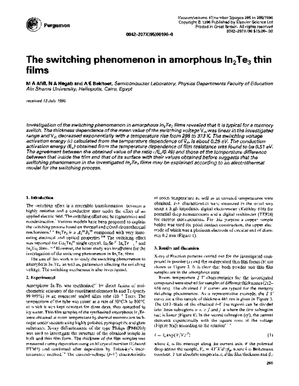
holder was used for point contact construction, the upper electrode of which was a platinum electrode of circular end of diameter 0.2 mm (Figure 1).
3. Results and discussion
X-ray diffraction patterns carried out for the investigated compound in powder (a) and the as-deposited thin film forms (b) are
shown in Figure 2. It is clear that both powder and thin film
samples are in the amorphous state.
Room temperature Z-I/ characteristics for the investigated
compound were studied for samples of different thicknesses (212654 nm). The obtained Z-V curves are typical for the memory
switching phenomenon. As a representative example, the Z-V
curve for a film sample of thickness 461 nm is given in Figure 3.
The OFF-State of the obtained Z-V (oa region) can be divided
into three subregions o-e, e-f andf-a where the first subregion
(ae) is linear (Figure 4). In the second subregion (ef), the current
increases exponentially with the square root of the voltage
(Figure 5(a)) according to the relation”~‘*
Z = Z, exp( V/ VJ”)
(1)
where Z, is the intercept along the current axis, I’ the potential
drop across the sample, V, = 4T2k2d2/&,f where k is Boltzmann
constant, T the absolute temperature, d the film thickness and &r
265
�MA Afifi et al: In,Te, thin films
n
d = 461 nm
Figure 3. I-V
characteristic curve for InzTe, film of thickness 461 nm.
Figure 1. Schematic representation of the cell used for I-V measurements
1--co-axial cable, 2 -a brass plate, 3 -teflon plated 4 -two brass rods,
5 -base of the cell made of brass, 6 -holder of platinum electrode, 7 slight spring, 8 - the platinum electrode, 9 -lower copper brass electrode, IO -the substrate and 11-the thin film layer.
&/@
A0
5
l
10
I
15
I
20
I
25
I
30
v (volts)
Figure 4. OFF state I-V characteristic curve for In,Te, film of thickness
461 nm.
-
80
70
60
50
40
30
20
Figure 2. X-ray diffraction patterns for In,Te, (a) Powder form (b) Asdeposited films.
the Poole-Frenkel
coefficient. It was found that values of Z, and
V,, in eqn (1) are 2 x lo-’ A and 1.07 V, respectively as obtained
from Figure 5(a). In the third subregion (fu) the current is an
exponential function of voltage (Figure 5(b)) according to the
relation:“,”
I = Z, exp( V/V,)
(2)
where values of I, and V, are 1.7 x lo-’ A and 8.89 V, respectively.
The switching voltage was measured for every film sample at
different points uniformly distributed throughout the surface of
the film and their mean value was calculated. The mean value of
switching voltage Ythwas determined for film samples of different
thicknesses in the range (212-654 nm) at room temperature. Z-V
characteristic curves for which Vth,
is equal to p,;h, were obtained
and are illustrated in Figure 6 for all the investigated thicknesses.
266
The obtained thickness dependence of vL;his linear in the investigated range as is clear from Figure 7. The slope of the obtained
line of thickness dependence represents the mean value of the
threshold field &,, (6.67 x lo7 V/m). The observed relation of
thickness dependence of rC,, agrees with previous observations
for different amorphous systems. “Jo” The variation of PC,,with
thickness is investigated
also at elevated temperatures.
The
obtained results are also illustrated in Figure 7. It is clear that
vt,, increased also linearly with thickness at elevated temperatures
in the investigated range. Values of &, decreased from 6.67 x 10’
to 9.1 x lo6 V/m with increasing temperature from 298 to 373 K.
The temperature dependence of the Z-V characteristics
of the
investigated In,Te, compound was studied in the range 298-378
K for films of different thicknesses in the range 212-654 nm. As
a representative
example the obtained Z-V curves for a film
sample of thickness 461 nm are shown in Figure 8. The obtained
parallel straight lines for the relation of In vt,, vs l/r (Figure 9)
indicates that vrh decreases exponentially
in the investigated
ranges of temperature
and thickness satisfying the following
relation:
�MA Afifi et al: InZTe, thin films
-12
r
(b)
I
0
I
I
200
400
Thickness
I
600
d (nm)
Figure 7. Thickness dependence of the mean value of the switching
for In,Te, films at different temperatures.
-13
voltage
5
I-50
-
-14
.
10
t P-2
I
I
I
I
l
15
20
25
30
+
o
A
0
v
I.oo
(volts)
Figure 5. (a) Dependence of In I on V ‘P for In,Te, film of thickness 461
nm. (b) Dependence of In I on V for In,Te, film of thickness 461 nm.
-
?
5%
25
40
60
80
105
50-
l 212
A 255
+ 315
0 390
o 461
0 523
x 654
3
10
20
30
L
0
v
40
v (volts)
Figure 6. I-V characteristic
nesses.
Fth = V,exp(~/kT)
(volts)
Figure 8. I-V characteristic
curves for film In*Te, films of thickness
nm at different temperatures.
curves for film In*Te, films of different
thick-
461
of the obtained lines of Figure 9 (0.255 eV) is thickness independent in the investigated range.
The mean value of the film resistance R was measured as a
function of temperature
in the range 298-378 K for different
film thicknesses in the range 212-654 nm simply by dividing the
potential drop across the sample by the current passing through
it within the linear part of the OFF-State
of the corresponding
I-V characteristic
curves for different points uniformly
distributed on the whole surface of the film and taking their mean
value. The results obtained for the temperature
dependence of
sample resistance are illustrated in Figure 10 as In R vs 1/T which
yields straight lines satisfying the following relation:
(3)
Where E is the switching voltage activation energy, and 1 the
absolute temperature.
The value of E calculated from the slopes
i? = Cexp(E,/kT)
Where E,, is the electrical
(4)
conduction
activation
energy, and C a
267
�MA AMi et al: In2Te3 thin films
Table 1. Values of ATbrea,.dawn
for In,Te, films at different temperatures
d W)
212
A 255
+ 315
0 390
0 461
0 523
x 654
l
I-
T W)
ATbreakdown
W)
298
313
333
353
373
14.7
16.9
19.1
21.5
24.0
can be understood
in terms of an electrothermal
model which
can be solved to a certain extent by finding a stationary state
solution for the heat transport equation.
= aE2 + V(uVT)
Cg
the charge conservation
!.5
I
I
I
I
2.7
2.9
3.1
3.3
ldp-_=
-idE
1000/T (K-l)
Figure 9. Plots of In vt;hvs lOOO/Tfor In,Te, films of different thicknesses.
d @ml
(6)
equation:
v
‘E
where C is the heat capacity, u the thermal conductivity,
E the
electric field, p the charge density and cr the electrical conductivity
which is given by:
o = (T, exp(E,/kT)
212
A 255
+ 315
o 390
0 461
(7)
(8)
l
In the case of steady state breakdown,
the time derivative of
temperature (dT/dt) can be neglected for the solution of eqn (6).
Hence, the heat conduction
equation for a small difference
(AT = T,,,- TS) between the temperature
at the middle of the
specimen T,,, and that of the surface T, gives?
lp:
8r~+aE2=0
9
(9)
where d is the thickness of the sample.
The steady state breakdown occurs when the amount of heat
generated by Joule-heating
cannot be removed by thermal conduction and the temperature difference necessary for breakdown
can be obtained from the equation:24,2s
A Tbreakdown= T21(-Wk)
I
I
I
I
2.7
2.9
3.1
3.3
1000/T
(K-t)
Figure 10. Plots of In R vs lOOO/Tfor In,Te, films of different thicknesses.
constant.
The value of E,, calculated from the slopes of the
parallel lines obtained (0.51 eV) is independent
of sample thickness in the investigated ranges. The calculated value of the ratio
c/E, (0.49) agrees well with that obtained previously”S’9-25 for
other amorphous semiconducting
films. It is also in good agreement with the value of (t/E,) derived theoretically on the basis of
an electro-thermal
model23 for the switching process. From eqns
(3) and (4) and taking into account that ~/E,,=0.5, we obtain the
following equation:
V&/R
= constant
(5)
This implies that the power dissipated during the switching process is constant.
The observed temperature
dependence
of switching voltage
268
(10)
According to this equation and using the value of E,, ATbreakdown
was calculated for In,Te, films at different temperatures
and the
obtained values are given in Table 1. It is clear that the obtained
with previous
values of ATbreakdownare in good agreement
for amorphous semiconducting
films. Also taking
results ‘9-22,2G26
into account the good agreement
of the obtained value of
(c/E,,=O.49)
mentioned
above with both values obtained
earlier ‘S22.24--26
and its value derived theoretically for the breakdown process, it can be concluded that the observed memory
type switching in In2Te, films can be satisfactorily explained according to electrothermal
breakdown process.
References
‘S R Ovshinsky, Phys Rev Left, 21, 1450 (1968).
’ H Fritzsche, S R Ovshinsky, J Non-tryst solids, 4,464 (1970).
’ K W Boer, S R Ovshinsky, J App Phys, 41,6 (1970).
4 D M Kroll, M H Coher, J Non-Crysf Solids, S-10, 544 (1972).
5 S A Hussein and A T Nagat, Phys St Sol (a), 114, K205 (1989).
6A A Zahab, M Abd-Lefdil and M Cadene, Phys St Sol (a), 115, 49 1
(1989).
�MA AMi et al: In,Te, thin films
7V A Petrusevich and V M Sergeeva, Sov Phys -Solid
State 2, 2562
(1961).
a A A Zahab, M Abd-Elfddil and M Cadene, Phys St Sol (a), 117, K103
‘* G A Denton, G M Friedman and I F Schetzima, J App Phys, 46,3044
(1975).
I9M A Afifi, N A Hegab, H H Labib and M Fadel, Ind J Pure and Applied
(1990).
9S Sen and D N Bose, Solid State Comm, 50, 39 (1984).
‘OS I Aliev, G M Niftiev, F I Pliev and B G Tagiev, Sov Phys Sem, 13,
Phys, 30,211 (1992).
“M A Kenawy, A E El-Shazly, M A At%, M A Zayed and H A ElZahid, Thin Solid Films, 200,203 (199 1).
” M A Afifi, H H Labib, A H Abou El-Ela and K A Sharaf, App Phys
A, 46, 113 (1988).
22F Abd El-Salam, M A Afili and E Abd El-Wahab, Vacuum, 41, 17
(1993).
23M Fadel, PhD Thesis, Ain Shams University, 1987.
24R Mehra, R Shyam and P C Mathur, J Non-tryst Solids, 31,435 (1979).
2sK Shimakova, Y Inagaki and T Arizumi, Jup J App Phys, 12, 1043
340 (1977).
I’ M A Afifi, H H Labib, N A Hegab, M Fade1 and A E Bekheet, Indian
J Pure and Appiied Physics, 33, 129 (1995).
‘*A Chenys and V Lisauskas, Lith Phys J, 31,237 (1991).
I3S Balevicius, A Cesnys and A Deksnys Phys St Sol (a), 35, K41 (1976).
I4S Balevicius, A Cesnys and A Deksnys Phys St Sol (a), 32, Kl 1 (1975).
“V P Zhuze, V M Sergeeva and A I Shelykh, Sov Phys -Solid State, 2,
2545 (1961).
16S Tolansky, Introduction to Interferometry.
Longman Group (1955).
“M Burglman Solid State Electronics, 20, 523 (1977).
(1973).
x G C Vezzoli and I M Pratt, Thin solidfi/ms,
14, 161 (1972).
269
�
 Ashraf Bekheet