IEEE TRANSACTIONS ON INSTRUMENTATION AND MEASUREMENT, VOL. 53, NO. 6, DECEMBER 2004
1479
Detective Quantum Efficiency [DQE(0)] of CZT
Semiconductor Detectors for Digital Radiography
G. C. Giakos, S. Suryanarayanan, R. Guntupalli, J. Odogba, N. Shah, S. Vedantham, S. Chowdhury, K. Mehta,
S. Sumrain, N. Patnekar, A. Moholkar, V. Kumar, and R. E. Endorf
Abstract—In this paper, the detective quantum efficiency (DQE)
of cadmium zinc telluride (CZT) detector samples for digital radiography has been measured. Specifically, this study is aimed at investigating the zero-frequency DQE(0) under different X-ray tube
and detector parameters. The experimental results of this study indicate that the DQE(0) of the CZT samples is strongly dependent
upon the irradiation geometry. This is attributed to the incomplete
charge collection process, which can be further improved by controlling the purity of the samples and the contact type.
Index Terms—Detective quantum efficiency, digital radiography, semiconductor detectors.
I. INTRODUCTION
LAT-PANEL image sensor arrays are being developed for
medical imaging applications [1]–[5], [7]–[12], [17]–[32].
These systems are comprised of large-area pixel arrays that use
matrix addressing to read out charges resulting from X-ray absorption in the detector medium. There are two methods for
making flat panel image sensors. In the indirect method [1], [9],
[10], a phosphor converter absorbs the incident X-rays and emits
visible light, which is converted by an a-Si:H p-i-n photodiode
into an electronic image. This process is inefficient and can lead
to increased image noise, particularly when signals are low. The
direct method [2], [17]–[32] uses a photoconductive layer to
absorb X-rays and collect the ionization charge which is subsequently read out by an active matrix array. The direct method
has a higher intrinsic resolution compared to the indirect method
because it avoids the X-ray to light conversion stage.
The primary advantages of photoconductors for good quality
imaging include efficient radiation absorption, large band gap
energy which limits the thermal generation of charge carriers
in the bulk, good linearity, good charge transport properties,
high stability, high sensitivity, and wide dynamic range. Lead
F
Manuscript received June 15, 2003; revised June 15, 2004.
G. C. Giakos and S. Sumrain, are with the Imaging Systems, Detectors
and Sensors Laboratory, Department of Electrical and Computer Engineering, The University of Akron, Akron, OH 44325-3904 USA (e-mail:
giakos@uakron.edu).
S. Suryanarayanan, R. Guntupalli, J. Odogba, N. Shah, S. Vedantham,
S. Chowdhury, K. Mehta, N. Patnekar, and A. Moholkar are with the Department of Biomedical Engineering, The University of Akron, Akron, OH
44325-0302 USA.
V. Kumar is with the Imaging Systems, Detectors and Sensors Laboratory,
Department of Electrical and Computer Engineering, Department of Electrical
and Computer Engineering, The University of Akron, and the Division of Engineering and Applied Mathematics, The University of Akron, Akron, OH 443250302 USA.
R. E. Endorf is with the Department of Physics, University of Cincinnati,
Cincinnati, OH 45221 USA.
Digital Object Identifier 10.1109/TIM.2004.834590
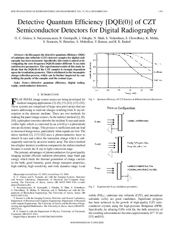
Fig. 1.
Quantum efficiency of CZT detectors at different detector thicknesses.
Fig. 2.
Experimental X-ray irradiation geometries.
iodide PbI , cadmium zinc telluride (CZT), and amorphous
selenium (a-Se) are good candidates. Significant progress
has been achieved in the growth of high-quality CZT semiconductor crystals using the high-pressure Bridgman (HPB).
Specifically, by alloying CdTe with Zn, the bulk resistivity of
-cm
the resulting semiconductor becomes approximately
[13] and[14].
0018-9456/04$20.00 © 2004 IEEE
�1480
IEEE TRANSACTIONS ON INSTRUMENTATION AND MEASUREMENT, VOL. 53, NO. 6, DECEMBER 2004
CZT semiconductor detectors are potential candidates for
medical imaging applications [29]–[32] due to the high energy
absorption efficiency (high atomic number and high density)
Zn Te (CZT) has
of the semiconductor medium. In fact, Cd
high stopping power due to its high mass density (5.8 g/cm )
, Zn
,
and effective atomic number Z of 49.6 (Cd
and Te: 52) [31]. In fact, the plot of Fig. 1 highlights the
high quantum efficiency of CZT systems at different detector
thicknesses. In general, comparing the performance of CZT
detectors with other photoconductors, the conversion energy
W is 20 eV at an applied electric field of 30
m for a-Se;
5 eV for CZT and PbI . Furthermore, the conversion energy
of a-Se is a function of the applied electric field. Because of
high W , the DQE of the a-Se-based system is less tolerant to
electronic noise than PbI and CZT. In addition, the DQE(0)
of the a-Se-based fluoroscopic system is
compared to
for the CZT-based system. Though the leakage current
in the CZT-based system is higher (
times) compared
to the a-Se-based system, the low W of 5 eV and the short
integration time of 33 ms/frame (at a frame rate of 30 frames/s)
negates, to a certain extent, the detrimental effects of the larger
leakage current and does not degrade the DQE significantly,
particularly for exposure levels between 0.5 and 2 R.
In this paper, the zero-frequency detective quantum efficiency
[DQE(0)] of a solid-state CdZnTe detector was measured under
different experimental conditions, and the system’s DQE was
measured under each of those conditions. A strong dependence
of the DQE with the irradiation geometry is observed which is
attributed to the poor collection efficiency of the CZT samples.
II. ZERO-FREQUENCY DETECTIVE QUANTUM
EFFICIENCY [DQE(0)]
DQE is a measure of the incident quanta detected by any
imaging system. It gives an indication of the system’s effectiveness in detecting an input signal and faithfully reproducing it
at the output stage. The DQE depends upon a number of inherent detector factors, such as the quantum efficiency, absorption efficiency, and collection efficiency of the detecting system.
The static or zero-frequency DQE implies that the source and
the detecting element are always static with respect to each
other.
In simple terms, the basic definition of DQE can be stated as
the ratio of the signal to noise at the detector’s output to that of
the signal-to-noise ratio (SNR) at the input of the detector. It is
represented as follows:
DQE
SNR
SNR
(1)
If we consider an ideal quantum process, the input SNR can be
represented as
SNR
(2)
Hence
SNR
(3)
TABLE I
Fig. 3.
Schematics of the current-sensitive preamplifier electronics.
where
is the number of incident X-ray quanta. For a conventional film, the slope of the characteristic curve is given as
, where
is the change in output density level, and
is the fraction of incident quanta.
represents the output noise over this range, the output
If
noise in terms of exposure can be represented as
Output noise
(4)
Hence, the output SNR can be represented as
SNR
(5)
is the X-ray signal.
where
The DQE can be defined as
DQE
SNR
SNR
(6)
III. EXPERIMENTAL DETERMINATION OF DQE(0)
In this paper, the output SNR from three different detector
configurations was studied based on the detector’s irradiation
geometry.
1) The X-ray beam was incident to the negative electrode of
the detector, and the signal was collected from the X-ray
incident surface. (Configuration 1).
�GIAKOS et al.: DETECTIVE QUANTUM EFFICIENCY [DQE(0)] OF CZT SEMICONDUCTOR DETECTORS.
Fig. 4. DQE(0) of a 0.3-mm-thick detector versus applied peak voltage at
100 mAs, with a 75-�m slit, and a voltage-to-voltage-instrumentation amplifier
(INA111) at different irradiation geometries.
2) The X-ray beam was incident to the positive electrode of
the detector, and the signal was collected from the X-ray
incident surface. (Configuration 2).
3) The X-ray beam was incident to the negative electrode of
the detector, and the signal was collected from the side
opposite to the X-ray incident surface (Configuration 3).
The three configurations presented in this paper are shown in
Fig. 2.
In this paper, the DQE(0) of a solid-state CdZnTe detector
was measured under different experimental conditions, and the
system’s DQE was measured under each of those conditions. To
measure the performance characteristics of the detector under
these conditions, a technique was adopted in which the DQE of
a photodiode or phosphor screen is defined as
DQE
SNR
(7)
where SNR is the output SNR at the preamplifier output, A
is the incident photon
is the active area of the detector,
fluence over a period of 1 s, and is the noise bandwidth of
the preamplifier and sampling noise bandwidth. can also be
represented as
(8)
1481
Fig. 5. DQE(0) of a 0.3-mm-thick detector versus square root of tube current
at 100 mAs with a 75-�m slit and a voltage-to-voltage-instrumentation amplifier
(INA111) at different irradiation geometries.
where
is the preamplifier and sampling transfer function,
is the initial value at zero frequency, and is the sampling
interval. The experimental parameters of the detector system are
tabulated in Table I.
The amplifiers were selected on the basis of their low noise,
high input impedance, sensitivity, and good overall performance characteristics. A fourth-order Butterworth filter with
a 3-dB rolloff frequency at 25 kHz was designed. The filter
incorporated LM358P and AD820 operational amplifiers. Care
was taken to minimize stray capacitance by using cables of
short length. Resistors with low noise (less than 0.5 dB above
thermal noise) were chosen to reduce the overall system noise.
Guarding was employed around the amplifier inputs in order to
decrease the noise and baseline instability caused by the surface
leakage current of the circuit board. The complete electronics
system was housed in an electromagnetically shielded box
to avoid interference from external sources. In Figs. 4–6, the
DQE(0) characteristics of a 0.3-mm detector, with a 75- m
slit and a voltage-to-voltage amplifier electronics system, are
shown for three different detector configurations. Similarly, the
DQE(0) characteristics of a 0.3-mm detector, with a 75- m slit
and a current-sensitive A250 amplifier electronics system, are
shown for three different detector configurations in Figs. 7–9.
�1482
IEEE TRANSACTIONS ON INSTRUMENTATION AND MEASUREMENT, VOL. 53, NO. 6, DECEMBER 2004
Fig. 6. DQE(0) of a 0.3–mm-thick detector versus applied bias voltage at
100 mAs with a 75-�m slit and a voltage-to-voltage-instrumentation amplifier
(INA111) at different irradiation geometries.
It is observed that the configuration two exhibits a statistically
higher DQE(0) when compared to the other configurations.
This is attributed to the fact that the detected signal contains
contributions from detected electrons and induced charge from
the electrons moving in opposite directions. Preliminary measurements indicate that for larger drift distances, the opposite
phenomenon is true. The DQE dependence upon the irradiation
geometry can be explained in terms of Hecht’s [31]. This is
an indicator of an incomplete collection process due to the
impurities in the CZT samples and because of the ion transport
parameters, such as low ion mobility.
The SNR of the preamplifier output is related to the quantum
noise and preamplifier noise bandwidth. The effects of the
system electronics on SNR were studied by assessing the
performance of a voltage-to-voltage instrumentation amplifier
(INA111) and a current-sensitive preamplifier (A250) on the
basis of their output SNR. A schematic of the current-sensitive
A250 preamplifier is shown in Fig. 3. The noise of each preamplifier system and electronics were recorded and stored on a
PC. The analog-to-digital converter sampling rate remained the
same for all measurements. The data were later imported into a
signal processing package (MATLAB), and a Fourier transform
was performed to obtain the frequency spectrum of the noise.
The sampling interval was determined by using the sampling
rate and number of data points recorded. Equation (8) was used
to determine the noise bandwidth.
Fig. 7. DQE(0) of a 0.3-mm-thick detector versus applied peak voltage at 100
mAs with a 75-�m slit and a current-sensitive preamplifier (A250) at different
irradiation geometries.
The incident fluence was computed experimentally from the
values of incident exposure over a period of 1 s. A Nuclear
Associates (Cleveland, OH) exposure meter, Red Check Plus
was used for this purpose. An active area equivalent to the
area of the detector was exposed to incident radiation from
the X-ray system over a period of 1 s. The exposure readings
were recorded in terms of milliroentgens per second and later
converted into fluence by using the following conversion:
J kg R
(9)
where
J, kg, and R Joules, kilograms, and Roentgen, respectively;
incident photon fluence (photons per square
centimeter);
incident exposure (Roentgen);
energy (Joules);
attenuation coefficient in air cm g .
The value of
and
were determined from single
photon emission computed tomography (SPECT) simulations.
Hence, by estimating all the above parameters, the DQE was
determined by means of (6).
�GIAKOS et al.: DETECTIVE QUANTUM EFFICIENCY [DQE(0)] OF CZT SEMICONDUCTOR DETECTORS.
Fig. 8. DQE(0) of a 0.3-mm-thick detector versus square root of tube current
at 100 mAs with a 75-�m slit and a current-sensitive preamplifier (A250) at
different irradiation geometries.
An X-ray system manufactured by Philips Medical Systems
was used as the source of radiation. The X-ray system generator tube was a three-phase 12-pulse PICKER 612 and Dunlee
PX-18K2-AQ, respectively. The intrinsic filter of the X-ray
tube was 3 mm of aluminum. The anode target angle of the
. In this paper, an X-ray tube focal spot
X-ray system was
of 0.6 mm was used.
An adjustable collimator was set at 75 m. The collimator’s
edges were made from 2–mm-thick tungsten rods and were
rounded to minimize scattering. The height of the collimator
was 10 cm.
As mentioned earlier, two preamplifier systems, namely, a
voltage-to-voltage-instrumentation amplifier INA111 manufactured by Burr-Brown and a current-sensitive preamplifier
A250 manufactured by AMTEK, were used in this study. A
field-effect transistor (FET) 3SK156 was placed at the input
of the preamplifier. This serves to increase the input resistance
of the preamplifier, as well as to achieve the lowest noise
performance, by matching with the detector capacitance. This
experimental evaluation was conducted under the same conditions, and their performance characteristics in terms of output
SNR were evaluated.
A statistical analysis of the data was done with a null hypothesis that the treatments had no significant effect on the
1483
Fig. 9. DQE(0) of a 0.3-mm-thick detector versus applied bias voltage at 100
mAs, with a 75-�m slit and a current-sensitive preamplifier (A250) at different
irradiation geometries.
DQE(0) with a level of significance of 0.05. The data were
analyzed by using a randomized complete block analysis of
variance (ANOVA). An analysis was performed to check for
significant differences between the three configurations for a
0.3-mm detector. The analysis was done separately for each
of the amplifier electronics. A significant difference was obtained, and hence, the null hypothesis was rejected. Further,
a post-priori Tukey test of the means was performed at a
significance level of 0.05, and results indicated the presence of
significant differences between detector configurations for both
amplifier electronics. A similar analysis was also carried out
to identify significant differences between the DQE(0) values
for the same configuration between two different amplifier
electronics under the same experimental conditions. The results
indicated a significant difference in each case at a level of 0.05,
thus rejecting the null hypothesis that no difference was present
among the treatments.
IV. CONCLUSION
The experimental results of this study indicate that the
DQE(0) of the CZT samples is strongly dependent upon the
irradiation geometry. This is attributed to the incomplete charge
collection process, which can be further improved by controlling the purity of the samples and the contact type.
�1484
IEEE TRANSACTIONS ON INSTRUMENTATION AND MEASUREMENT, VOL. 53, NO. 6, DECEMBER 2004
REFERENCES
[1] L. E. Antonuk, J. Yorkston, and W. Huang, “A real time, flat-panel,
amorphous silicon, digital X-ray imager,” Radiographics, vol. 15, pp.
993–1000, 1995.
[2] G. C. Giakos, “Multimedia Detectors for Medical Imaging,” U.S. Patent,
6 207 958, Mar. 23, 2001.
[3] P. C. Jones, D. J. Drost, M. J. Yaffe, and A. Fenster, “Dual-energy
mammography: Initial experimental results,” Med. Phys., vol. 12, pp.
297–304, 1985.
[4] P. C. Jones and M. J. Yaffe, “X-ray characterization of normal and neoplastic breast tissues,” Phys. Med. Biol., vol. 32, pp. 675–695, 1987.
[5] G. C. Giakos, “Hybrid detection trends in medical imaging,” in Physics
Seminar Series. Ottawa, ON, Canada: Herzberg Lab. Phys., Carleton
Univ., 1997.
[6] D. Allison, A. Epenetos, P. Jalas, Z. Karim, M. Meyers, R. Orava, J.
Pythia, J. Salonen, B. Sanghera, M. Sarakinos, T. Schulman, K. Spartiotis, I. Suni, and C. Tieliang, “A novel semiconductor pixel device and
system for X-ray and gamma ray imaging,” in Proc. IEEE Nucl. Sci.
Symp., vol. 2, 1997, pp. 1248–1250.
[7] T. Asaga et al., “Breast imaging: Dual-energy projection radiography
with digital radiography,” Radiology, vol. 164, pp. 869–870, 1987.
[8] L. E. Antonuk et al., “Performance evaluation of a large area, 97 �m
pitch: Indirect detection active matrix flat-panel imager (AMFPI) for
radiography and fluoroscopy,” Radiology, vol. 209, pp. 357–357, 1998.
[9] L. E. Antonuk et al., “Performance limits of high resolution large area
active matrix flat-panel imagers (AMFPI’s),” Radiology, vol. 209, pp.
581–581, 1998.
[10] L. E. Antonuk et al., “Strategies to significantly enhance performance
of active matrix flat-panel imagers (AMFPI’s),” Radiology, vol. 209, pp.
358–358, 1998.
[11] E. L. Baker, A. R. Cowen, R. Kemner, and R. Bastiaens, “A physical
image quality evaluation of a CCD-based X-ray image intensifier digital
fluorography system for cardiac applications,” Proc. Int. Soc. Opt. Eng.,
vol. 3336, pp. 430–441, 1998.
[12] C. D. Bradford, W. W. Peppler, and J. T. Dobbins, “Performance characteristics of a kodak computed radiography system,” Med. Phys., vol.
26, no. (1), pp. 27–37, 1999.
[13] J. F. Butler, F. P. Doty, and C. L. Lingren, “CdZnTe gamma ray detectors,” IEEE Trans. Nucl. Sci., vol. 39, pp. 605–609, Aug. 1992.
[14] J. F. Butler, S. J. Friesenhahn, C. Lingren, W. L. Ashburn, and W. Dillon,
“CdZnTe detector imaging array,” Proc. Int. Soc. Opt. Eng. , vol. 1896,
pp. 30–37, 1993.
[15] J. F. Butler and B. Apotovsky, “Sub-keV resolution detection with
Cd
zn Te detectors,” Proc. Int. Soc. Opt. Eng., vol. 2009, pp.
121–127, 1994.
[16] J. W. Byng, J. G. Mainprize, and M. J. Yaffe, “X-ray characterization
of breast phantom materials,” Phys. Med. Biol., vol. 43, pp. 1367–1377,
1998.
[17] S. Chowdhury, “Signal production of gas-microstrip detectors for medical [14] imaging,” M.S. Thesis, Univ. Akron, Akron, OH, 1997.
[18] G. C. Giakos, F. A. DiBianca, R. J. Endorf, D. J. Wagenaar, S. Devidas,
H. Zeman, J. Laughter, S. Nagarajan, A. Mahmud, and S. Collipara, “Engineering aspects of a kinestatic charge detector,” J. X-ray Sci. Tech., vol.
5, pp. 181–201, 1995.
[19] P. C. Jones and M. J. Yaffe, “Theoretical optimization of dual-energy
X-ray imaging with application to mammography,” Med. Phys., vol. 12,
pp. 289–296, 1985.
[20] G. C. Giakos, “Multidensity and Multi-atomic Number Detector Media
for Applications,” U.S. Patent 6, 069, 362, May 30, 2000.
[21]
, “Multidensity and Multi-Atomic Number Detector Media for Applications,” Eur. Patent 99 918 933.5-2213, Dec. 28, 2000.
[22] G. C. Giakos, S. Chowdhury, N. Shah, K. Mehta, S. Sumrain, N. Patnekar, L. Fraiwan, and R. Nemer, “Signal evaluation of a novel dual-energy multimedia imaging sensor,” IEEE Trans. Instrum. Meas., vol. 51,
pp. 949–953, Oct. 2002.
[23] G. C. Giakos, S. Chowdhury, N. Shah, S. Vedantham, A. G. Passerini,
S. Suryanarayanan, N. Shah, K. Mehya, S. Sumrain, and C. Scheiber,
“Signal-to-noise measurements utilizing a novel dual-energy multimedia detector,” IEEE Trans. Instrum. Meas., vol. 50, pp. 911–914,
Aug. 2001.
[24] G. C. Giakos, “Hybrid detection trends in medical imaging,” in Physics
Seminar Series. Ottawa, ON, Canada: Herzberg Lab. Phys., Carleton
Univ., 1997.
[25]
, “A slot-scanned detector operating on gas-solid state imaging
principles,” in Proc. IEEE Instrum. Meas. Tech., vol. 1, 1998, pp.
352–357.
[26] G. C. Giakos, S. Chowdhuri, B. Pillai, P. Ghotra, S. Vedantham, and A.
Dasgupta, “Novel multimedia detectors for medical imaging,” Proc. Int.
Soc. Opt. Eng., vol. 2708, pp. 759–767, 1996.
[27] G. C. Giakos, S. Vedantham, S. Chowdhury, and B. Pillai, “Novel hybrid
imaging modalities,” Proc. Int. Soc. Opt. Eng., vol. 3032, pp. 476–476,
1997.
[28] G. C. Giakos, S. Chowdhury, A. Dasgupta, A. Dasgupta, P. Pillai, P.
Ghotra, S. Suryanarayanan, and J. Odogba, “Study of a gas microstrip
detector for medical applications,” Proc. Int. Soc. Opt. Eng. (SPIE), pp.
459–468, 1997.
[29] G. C. Giakos, B. Pillai, S. Vedantham, S. Chowdhury, A. Dasgupta, D.
B. Richardson, P. Ghotra, R. J. Endorf, A. Passalaqua, and W. J. Davros,
Zn Te detectors for digital radiography,” J.
“Optimization of Cd
X-ray Sci. Tech., pp. 37–49, 1997.
[30] G. C. Giakos, B. Pillai, S. Vedantham, S. Chowdhury, J. Odogba, A. Dasgupta, V. Vega-Lozada, R. Guntupalli, S. Suryanarayanan, R. J. Endorf,
A. Passalaqua, and S. Kollipara, “Electric field dependence on charge
collection of CdZnTe X-ray detectors,” J. X-ray Sci. Tech., pp. 198–210,
1997.
[31] G. C. Giakos, S. Vedantham, S. Chowdhury, J. Odogba, A. Dasgupta,
B. Pillai, D. B. Sheffer, R. E. Nemer, R. Guntupalli, S. Suryanarayanan,
Zn Te deand V. Vega-Lozada, “Study of detection efficiency of Cd
tectors for digital radiography,” IEEE Trans. Instrum. Meas., vol. 47, pp.
244–251, Feb. 1998.
[32] G. C. Giakos, A. Dasgupta, S. Suryanarayanan, S. Chowdhury, S. VedanZn Te detectham, and B. Pillai, “Sensitometric response of Cd
tors for chest radiography,” IEEE Trans. Instrum. Meas., vol. 47, pp.
252–255, Feb. 1998.
G.C. Giakos Photograph and biography not provided at the time of publication.
S. Suryanarayanan Photograph and biography not provided at the time of publication.
R. Guntupalli Photograph and biography not provided at the time of publication.
J. Odogba Photograph and biography not provided at the time of publication.
N. Shah Photograph and biography not provided at the time of publication..
S. Vedantham Photograph and biography not provided at the time of publication.
S. Chowdhury Photograph and biography not provided at the time of publication..
K. Mehta Photograph and biography not provided at the time of publication.
S. Sumrain Photograph and biography not provided at the time of publication.
N. Patnekar Photograph and biography not provided at the time of publication.
A. Moholkar Photograph and biography not provided at the time of publication.
V. Kumar Photograph and biography not provided at the time of publication..
R.E. Endorf Photograph and biography not provided at the time of publication.
�
 George Giakos