Illlll llllllll II llllll lllll lllll lllll lllll lllll lllll lllll 111111111111111111111111111111111
US 20130089968Al
United States
c12) Patent Application Publication
c19)
Usenko
c10)
(43)
Pub. No.: US
Pub. Date:
2013/0089968 Al
Apr. 11, 2013
(54)
METHOD FOR FINISHING SILICON ON
INSULATOR SUBSTRATES
(76)
Inventor:
(21)
Appl. No.:
13/805,143
(57)
(22)
PCT Filed:
Jun.28,2011
(86)
PCT No.:
PCT/USll/42168
§ 371 (c)(l),
(2), (4) Date:
Dec.18,2012
A process for finishing an as transferred layer on a semiconductor-on-insulator structure or a semiconductor-on-glass (or
other insulator substrate) structure is provided by removing
the damaged surface portion of a semiconductor layer while a
leaving a smooth, finished semiconductor film on the glass.
The damaged surface layer is treated with an oxygen plasma
to oxidize the damaged layer and convert the damaged layer
into an oxide layer. The oxide layer is then stripped in a wet
bath, such as hydrofluoric acid bath, thereby removing the
damaged portion of the semiconductor layer. The damaged
layer may be an ion implantation damaged layer resulting
from a thin film transfer processes used to make the semiconductor-on-insulator structure or the semiconductor-on-glass
structure.
Provisional application No. 61/360,300, filed on Jun.
30, 2010.
Publication Classification
(51)
U.S. Cl.
CPC .................................. HOJL 2113065 (2013.01)
USPC .......................................................... 438/458
Alex Usenko, Painted Post, NY (US)
Related U.S. Application Data
(60)
(52)
Int. Cl.
HOJL 2113065
(2006.01)
ABSTRACT
121
122
- - - - - - - - - - - - - - - -
------
123
120
124
�Patent Application Publication
Apr. 11, 2013 Sheet 1 of 7
US 2013/0089968 Al
/100
104
102
Fig. 1
121
122
123
120
124
Fig. 2
�Patent Application Publication
Apr. 11, 2013 Sheet 2 of 7
US 2013/0089968 Al
-"'-124
122
t - - - - - - - - - - - - - - - - : f______ -132
- - - - - - - - - - - - - - - - - __,______ 134
102
-k.130
QRTセ@
Fig. 3
I
Mセ@
100{-=================- ZQセイR@
136
Fig. 4
125
�Patent Application Publication
Apr. 11, 2013 Sheet 3 of 7
US 2013/0089968 Al
Fig. 5
122C
Fig. 6
100
i22B
125
セ@
)
セ@
102
122C
Fig. 7
�Patent Application Publication
セPXN@
US 2013/0089968 Al
ii
1
.
セ@ セZ@ セ@
i'
i
v
'
セ@
ii i
ii i
/ii I
'' i
ir - - - --n-
i
- ---------- ---- ------+t _L____________L -- -- - -
-1
i
ii i
ii i
!
ii i
·セ@ セ@ - - - - - - - - - - --n-10 セiヲG@ --- - ---:i- - - - - - - - -- ---ri- ·t
10 0
セ@
;li i
ii
•
16.0
Thickness (nm)
Apr. 11, 2013 Sheet 4 of 7
4:0
0.1
,....セ@
;
1
10
100
Time {seconds)
Fig. 8
8.5
'
a.o - Mセ
i
''
i
::
!
! !
---- - - - - ---1--------------- ------- ------ ----- --H- -
7 .5
' '
70
セqLN@
Thickness (11 m) 6: 5 - --------------- ______J _____
--- =: セ@ セ@
!\---------- - - - --- - - ---L+-- -
セ@50Zセ@ - --------------- --------i-------- --- --- -- MKセ
i
!
4:5
セ@
)0
I
10
---- - - --
·100
---l---1- -- ii
l
i
1000
Pressure (rn Torr)
Fig. 9
YNPセM@
8.0-+-----+---+---+---1=-'e::............--l
WNPMKセ^Bャ@
Thickness (nm) 6.0
5. PMK⦅Lセャ@
4. PMセK\@
3.0-+---'---+---l----+---+----l
0
200
400
600
Power (watts)
Fig. 10
800
1000
�Patent Application Publication
Apr. 11, 2013 Sheet 5 of 7
US 2013/0089968 Al
/
/
/
..........
.,....
t::
N⦅セ@
c
(}';
(j)
iD
c
.Y..
0
/
102
..c
!-(I)
u
·x
0
/
/
,..
101
Oxidation Time (rnin)
.
,
Fig. 11
�""O
セ@
......
('D
=
......
セ@
'e
-........
Fig. 12
(')
セ@
......
0
Area 1
Area 2
Z--Rm1ge(nrn)
RMS (nrn)
Ra(nrn)
Z- RangEi(nrn)
Rrv'!S (nrn)
S",,_)
90.93
189.31
102.31
8.56
9.55
8.44
6J4
7.34
6.60
92.37
192.97
94.76
8.33
9.30
8.74
6.5f:i
7.23
6.85
80.96
185.60
85.18
S4
185.26
9.93
7.67
229.49
9.82
7.52
193.22
S1
S2
=
""O
=
O"
....
Area 3
Ra(nn1)
Z-Range(nrn)
rヲ|セs@
-....
sエ、セカ@
Ra(nrn)
f\veragE;
8.38
9.47
8.70
6.59
7.29
6.84
6.63
7.29
6.76
0.10
0.06
0.14
9.41
7.31
7.50
0.18
(nrn)
(')
セ@
......
0
=
セ@
セ@
:-:
......
......
N
0
......
(.H
1J1
Average Surface Roughness (nm)
nm
rnt---+-i ; セ@
6.75
6.50
セZ⦅Li@
.J...
1 I . l
81
1 .
S2
T
.L
'
l S3 I . l
f§
B
84
=-
('D
('D
......
O'I
0
......
......:i
c
1J1
N
0
......
(.H
---00
QO
"°
O'I
"°
>
......
QO
�Patent Application Publication
Apr. 11, 2013 Sheet 7 of 7
US 2013/0089968 Al
250
200
150
100
/
//
50
0
1
sn
S2
.j
0 left
!J Middle
D Right
Fig. 13
84
�US 2013/0089968 Al
Apr. 11, 2013
1
METHOD FOR FINISHING SILICON ON
INSULATOR SUBSTRATES
CLAIMING BENEFIT OF PRIOR FILED U.S.
APPLICATION
[0001] This application claims the benefit of priority under
35 U.S.C. §119 of U.S. Provisional Application Ser. No.
61/360300 filed on Jun. 30, 2010, entitled "METHOD FOR
FINISHING SILICON ON INSULATOR SUBSTRATES".
BACKGROUND
[0002] The present invention relates generally to an
improved finishing process for manufacturing semiconductor-on-insulator (SOI) substrates, more particularly for
removing damaged surface portions of semiconductor films
on SOI substrates produced using a thin film transfer process
to provide an undamaged, smoothened surface.
[0003] To date, the semiconductor material most commonly used in semiconductor-on-insulator structures has
been single crystalline silicon. Such structures have been
referred to in the literature as silicon-on-insulator structures
and the abbreviation "SOI" has been applied to such structures. Silicon-on-insulator technology is becoming increasingly important for high performance thin film transistors,
solar cells, and displays. Silicon-on-insulator wafers consist
of a thin layer of substantially single crystal silicon 0.01-1
microns in thickness on an insulating material. As used
herein, SOI shall be construed more broadly to include a thin
layer of material on insulating materials other than and
including silicon.
[0004] Various ways of obtaining SOI structures include
epitaxial growth of silicon on lattice matched substrates. An
alternative process includes the bonding of a single crystal
silicon wafer to another silicon wafer on which an oxide layer
of Si02 has been grown, followed by polishing or etching of
the top wafer down to a layer of single crystal silicon having
a thickness of several microns or greater. Further methods
include "thin film transfer" methods in which ions of gases
are implanted in a silicon donor wafer to create a weakened
layer in the donor wafer for separation (exfoliation) of a thin
silicon layer that is transferred and bonded to a handle or
support wafer. The support wafer can be another silicon
wafer, glass sheet, etc. The latter method of thin film transfer
involving gas ion implantation is currently considered advantageous over the former methods for producing thin films on
insulating handle substrates.
[0005] U.S. Pat. No. 5,374,564 discloses a thin film transfer
and thermal bonding process for producing SOI substrates
called "Smart Cut." Thin film exfoliation and transfer by the
hydrogen ion implantation method typically consists of the
following steps. A thermal oxide film is grown on a single
crystal silicon wafer (the donor wafer). The thermal oxide
film becomes a buried insulator or barrier layer between the
insulator/support wafer and the single crystal film layer in the
resulting of SOI structure. Hydrogen ions are then implanted
into the donor wafer to generate subsurface flaws. Helium
ions may also be co-implanted with the Hydrogen ions. The
implantation energy determines the depth at which the flaws
are generated and the dosage determines flaw density at this
depth. The donor wafer is then placed into contact and "prebonded" with another silicon support wafer (the insulating
support, receiver or handle substrate or wafer) at room temperature to form a tentative bond between the donor wafer and
the support wafer. The pre-bonded wafers are then heattreated to about 600° C. to cause growth of the subsurface
flaws resulting in separation of a thin layer or film of silicon
from the donor wafer. The assembly is then heated to a temperature above 1000° C. to fully bond the silicon to the
support wafer. This thin film transfer process forms an SOI
structure with a thin film of silicon bonded to a silicon support
wafer with an oxide insulator or barrier layer in between the
film of silicon and the support wafer.
[0006] As described in U.S. Pat. No. 7,176,528, thin film
transfer techniques have been applied more recently to SOI
structures wherein the support substrate is a glass or glass
ceramic sheet rather than another silicon wafer. This kind of
structure is further referred to as silicon-on-glass (SiOG),
although semiconductor materials other than silicon may be
employed to form a semiconductor-on-glass (SOG) structure.
Glass provides a cheaper handle substrate than silicon. Also,
due to the transparent nature of the glass, the applications for
SOI can be expanded to areas such as displays, image detectors, thermoelectric devices, photovoltaic devices, solar cells,
photonic devices, etc, that may benefit from a transparent
substrate.
[0007] The thin layer of semiconductor material (e.g., silicon) can be amorphous, polycrystalline, or of the single crystalline type. The amorphous and polycrystalline types of
devices are less expensive than their single crystal counterparts, but they also exhibit lower electrical performance characteristics. The manufacturing processes for making SOI
structures with amorphous or polycrystalline layers are relatively mature, and the performance of final products employing them is limited by the properties of the semiconductor
material. In contrast to the amorphous and polycrystalline
semiconductor materials, which are low quality semiconductors, single crystalline semiconductor material (such as silicon) is considered ofrelatively higher quality. Thus, the use of
such higher quality single crystalline semiconductor materials will enable the manufacture of higher quality, higher performance devices.
[0008] In thin film transfer fabrication processes for fabricating SOI and SOG substrates, a semiconductor film or layer
is exfoliated from a semiconductor donor wafer and bonded
to an insulating support substrate, such as a silicon wafer or
glass sheet. The surface of the exfoliated or "as transferred"
semiconductor film is not perfectly smooth. The as transferred film typically has a surface roughness of about 10 nm.
Moreover, the top portion of the as transferred film, for
example, tens of nm deep into the as transferred film, has a
large degree of crystal structure damage. This damage is a
result of the high dose ion implantation and the heat induced
exfoliation that are required to enable the film transfer process. During implantation, the ion species (e.g., hydrogen
ions, or hydrogen and helium ions) are accelerated into the
semiconductor crystal lattice. While moving through the
crystal lattice, the ions displace semiconductor atoms from
their regular locations in the lattice. The displaced semiconductor atoms are thus disruptions or damage in a properly
ordered lattice, i.e. they are defects in or damage to the overall
single crystalline media. Implanted ions eventually lose their
kinetic energy and come to rest in the lattice. These ions are
also defects in the crystal lattice, as they are not semiconductor atoms and they are not located in proper lattice locations.
Therefore, after ion implantation, the donor silicon substrate
will have hydrogen contaminated and displaced semiconductor atom damaged crystal regions within and around a range
�Apr. 11, 2013
US 2013/0089968 Al
2
of depths. Following exfoliation of the silicon exfoliation
layer, a portion of this contaminated and damaged region
remains on the as transferred semiconductor film or layer. As
a result, the surface of the as transferred semiconductor film
exhibits excessive surface roughness and crystal damage. The
surface roughness and crystal damage detrimentally effects
the fabrication and performance of electrical device formed
on or in the as transferred layer. Therefore, the rough and
damage portion of the surface of the as transferred semiconductor layer or film must be removed and the surface must be
smoothened.
[0009] There are several known surface removal and
smoothing methods. Chemical-mechanical polishing (CMP)
removal of damaged silicon is described in U.S. Pat. No.
3,841,031. The CMP polishing process involves holding and
rotating a thin flat wafer of semiconductor material against a
polishing surface under controlled pressure and temperature
in the presence of a flow of polishing slurry. When polishing
a relatively thin transferred semiconductor film on a relatively
thick substrate, however, the polishing action degrades the
thickness uniformity of the transferred film. Glass surface
variations are in orders of microns, while the film to be
smoothed is only fraction of a micron thick. Due to the relatively large size of the glass surface variations relative to the
thickness of the thin film, some areas of the transferred film
may get polished off completely with typical mechanical
polishing processes forming holes in areas of the film, while
other areas of the film may not be polished at all. A modified
CMP method for smoothing silicon-on-glass uses a small
computer-controlled polishing head, as is described, for
example, in U.S. Pat. No. 7,312,154, in order to uniformly
thin the film over high and low spots on the glass. This method
is not advantageous, as it has a low throughput and volume
manufacturing is not possible with this method.
[0010] Another problem with mechanical polishing processes is that they exhibit particularly poor results when rectangular SOI structures (e.g., those having sharp comers) are
polished. Indeed, the aforementioned surface non-uniformities are amplified at the comers of the SO I structure compared
with those at the center. Still further, when large SOI structures are contemplated (e.g., for photovoltaic applications),
the resulting rectangular SOI structures are too large for typical polishing equipment (which are usually designed for the
300 mm standard wafer size). Cost is also an important consideration for commercial applications of SOI structures. The
polishing process, however, is costly both in terms of time and
money. The cost problem may be significantly exacerbated if
non-conventional polishing machines are required to accommodate large SOI structure sizes.
[0011] Removal of the damaged portion of silicon film can
also be performed by etching, either wet or dry. For wet etch
of silicon, KOH can be used. For dry etch of silicon processing in CF4 plasma can be used. However, even though the
etching techniques provide removal of the damaged silicon,
they typically provide a conformal removal (e.g. the same
thickness of material is removed from high spots on the
surface as is removed from low spots on the surface), so the
surface of an etched silicon film remains rough and no
smoothening effect is achieved.
[0012] Isotropic etching of silicon would provide both
damaged material removal and surface smoothening. Isotropic etching of silicon can be performed in, for example,
so-called HNA solution, which is a mixture of hydrofluoric,
nitric, and acetic acids. However, the HNA is highly danger-
ous and toxic, and therefore it does not fit well to large scale
manufacturing. Also, a nitric oxide (laughing gas) is a
byproduct of silicon etching in the HNA. The nitric oxide is
highly aggressive and toxic, which make it not well suited for
the large scale manufacturing.
[0013] Also, in silicon-on-insulator (SOI) technology, thermal oxidation/strip cycles have been used to obtain SOI
wafers with a very thin top silicon film, much thinner than the
as-transferred silicon film. Thermal oxidation is a process
requiring temperatures 900° C. or higher. This cannot be used
for SiOG, as most glasses can only withstand temperatures up
to about 600° C.
[0014] Further steps in the process of fabricating SOI substrates, such as bonding, exfoliation, annealing and/ or polishing, may result in partial or total removal of implantationinduced crystal damage. Bonding and exfoliation steps are
usually performed at elevated temperatures, which drive any
residual hydrogen ions out of the lattice due to diffusion. In
order to completely heal the implant-induced damaged by
heating (e.g., annealing), the crystal has to be heated to a
temperature approaching the melting temperature of the crystal semiconductor material. For silicon, the melting temperature is 1412° C., and heating to about 1100° C. is required to
almost completely heal the post-implantation crystal damage.
During the process of fabricating a silicon-on-glass device,
annealing to temperatures above about 600° C. is prohibited
because most glasses can only withstand such high temperatures
[0015] Melting and re-crystallization of the exfoliated
semiconductor layer using excimer laser annealing is
described in international publication W0/2007 /142911. The
excimer laser beam melts a top portion of the semiconductor
layer while maintaining the glass substrate at a cooler temperature. This method results in poorer electrical characteristics within the annealed semiconductor material because the
melted part of the single crystalline material solidifies too
fast. In a regular Czochralski method of silicon growth, the
rate of growth is around 1 millimeter per minute. In contrast,
the re-growth rate of silicon melted and re-crystallized via an
excimer laser is about 1OE!4 times faster. The relatively slow
growth rate of the Czochralski method allows a nearly ideal
crystal lattice to grow. At faster growth rates, there is not
enough time for individual silicon atoms to diffuse to proper
positions. Many silicon atoms are thus frozen at irregular
locations, which means that they are structural defects in the
newly formed lattice.
[0016] In commonly owned U.S. patent application Ser.
No. 12/391,340 filed on Feb. 42, 1009, entitled Semiconductor on Insulator Made Using Improved Defect Healing Process, the damaged, single crystalline silicon layer of a siliconon-glass structure is implanted with silicon in a dose and at an
energy sufficient to amorphize an upper, damaged portion of
the single crystal silicon material, but not sufficient to amorphize the entire single crystal silicon layer. The pre-implanted
substrates are then annealed at a temperature in a range
between about 550° C. and 650° C. to transform the amorphous layer into a single crystalline layer. The lower, nonamorphized portion of the silicon layer serves as a seed for
solid phase epitaxial re-growth of the single crystal material.
This method reduces the amount of structural defects in the
damaged portion of silicon film, but it does not improve
surface roughness much. Thus, only one of two required
actions of film finishing is accomplished with this method.
�Apr. 11, 2013
US 2013/0089968 Al
3
[0017] For polysilicon annealing, the excimer laser technique is effective, as the polysilicon can be approximated as a
crystal with a very high level of structural defects. In an SOI
obtained by exfoliation of a single crystal semiconductor
layer, however, the initial number of defects of the semiconductor material is not as high as in polysilicon. While the
excimer laser annealing technique may heal some or all of the
initial defects in the semiconductor material, it introduces
new defects in about the same concentration as before the
annealing, or even higher. Thus, the excimer laser annealing
technique results in only a marginal improvement in the electrical properties of the exfoliated semiconductor layer.
[0018] An additional problem with laser annealing is that
the melted semiconductor material, such as silicon, is significantly denser than crystalline silicon (2.33 and 2.57 g/cm3
respectively). When the melted silicon solidifies after the
excimer laser scan, the difference between the respective
densities results in a characteristic, periodic fluctuation in the
thickness of the re-melted silicon. Thus, the excimer laser
annealed films are inherently non-smooth, which is a disadvantage.
[0019] For the reasons discussed above, none of the aforementioned techniques and processes for removing or otherwise correcting for damage to the semiconductor lattice structure has been satisfactory in the context of manufacturing
SOG structures. Thus, there is a need in the art for an
improved and economical process for finishing SOI structures, and in particular SOG structures, in order to both (1)
remove the damaged portion in the surface of the as transferred semiconductor layer created during ion implantation
and (2) smoothen (or finish) the surface of the as transferred
semiconductor layer.
SUMMARY
[0020] One or more features disclosed herein include
removal of the ion implant damaged surface portion or layer
of the exfoliated semiconductor layer obtained using a thin
film transfer process or other layer formation process. The
damaged layer is removed in a manner that will not degrade,
or otherwise damage a glass substrate supporting the semiconductor layer. In accordance with one or more embodiments disclosed herein, methods of forming a semiconductor
on glass structure, include: subjecting the as transferred semiconductor film to an oxygen plasma treatment to oxidize the
ion implant damaged layer, region or portion of the exfoliated
semiconductor layer; and then stripping the oxidized layer in
a wet bath, such as with a hydrofluoric acid solution, thereby
removing the damaged portion of the as transferred exfoliated
semiconductor layer.
[0021] According to an embodiment hereof, the method of
forming a semiconductor on glass structure may include the
steps of: subjecting an implantation surface of a semiconductor donor wafer to an ion implantation process to create an
exfoliation layer of the semiconductor donor wafer; bonding
the implantation surface of the exfoliation layer to a glass or
glass-ceramic substrate; separating the exfoliation layer from
the semiconductor donor wafer, thereby exposing a rough,
ion implantation damaged surface layer on the exfoliation
layer; subjecting the rough, damaged surface layer to oxygen
plasma to oxidize the damaged surface layer and convert the
damaged layer to an oxide layer; and stripping the oxide layer,
thereby removing the damaged layer and leaving a smoothened, finished surface on the exfoliation layer bonded to the
glass or glass ceramic substrate.
[0022] The exfoliation layer may be oxidized and stripped
to a depth sufficient to thin the exfoliation layer substantially
to a desired final or finished thickness in a single oxidize/strip
step or in multiple oxidize/strip steps or cycles.
[0023] The exfoliation layer may be oxidized and stripped
to a depth sufficient to remove the entire damaged layer in a
single oxidize/strip step. Alternatively, multiple oxidize/strip
steps or cycles may be employed to remove the damaged layer
bit by bit.
[0024] The oxygen plasma processing parameters is in a
range sufficient to oxidize an upper portion of exfoliation
layer closest to the at least one cleaved surface, while not
oxidizing a lower portion of the semiconductor material farther from the at least one cleaved surface.
[0025] The oxygen plasma treatment may be conducted in
a plasma generated at a frequency of 1 MHz or lower, from 1
MHz to 1 kHz, or about 30 kHz or lower.
[0026] The semiconductor donor wafer may be formed of
silicon (Si), germanium-doped silicon (Si Ge), silicon carbide
(SiC), germanium (Ge), gallium arsenide (GaAs), gallium
nitride (GaN), GaP, or InP.
[0027] According to other embodiments hereof, a method
is provided that includes forming a semiconductor on glass
structure, including the steps of: subjecting an implantation
surface of a semiconductor donor wafer to an ion implantation process to create an exfoliation layer of the semiconductor donor wafer; bonding the implantation surface of the
exfoliation layer to a glass substrate; separating the exfoliation layer from the semiconductor donor wafer, thereby
exposing an ion implantation damaged layer on the surface of
the exfoliation layer; characterized by the steps of: the subjecting the exposed damaged layer to oxygen plasma to oxidize the exposed damaged layer and convert at least a portion
of the exposed damaged layer to an oxide layer; and stripping
the oxide layer, thereby removing at least a portion of the
damaged layer.
[0028] The oxygen plasma processing parameters may be
one of: in a range sufficient to oxidize at least a portion of the
exposed damaged layer, while leaving at least a portion of an
undamaged lower portion of the semiconductor exfoliation
layer unoxidized; in a range sufficient to oxidize the exposed
damaged layer to a depth that is at least equal to or slightly
greater than a depth of the damaged layer; or selected to
oxidize the exposed damaged layer to a depth in a range from
about 10 nm to about 20 nm.
[0029] The plasma treatment may be conducted in a plasma
generated at one of: a frequency of 1 MHz or lower; a frequency of from 1 MHz to 1 kHz; a frequency of about 30 kHz
or lower; a frequency of about 13.56 MHz; or a frequency of
about 30 kHz.
[0030] The plasma treatment may be conducted in a direct
current plasma (zero frequency) with at least one of: a power
in a range from about 1 Watt/cm2 to about 50 Watts/cm2 ; a
pressure in a range from about 0.3 mTorrto about 300 mTorr;
and for a time in a range from about 0.5 minutes to about 50
minutes.
[0031] The semiconductor donor wafer may be formed of a
material selected from the group consisting of: gallium
nitride (GaN), silicon (Si), germanium-doped silicon (Si Ge),
silicon carbide (SiC), germanium (Ge), gallium arsenide
(GaAs), GaP, and InP.
[0032] A portion of the damaged layer may remain on the
exfoliation layer following oxygen plasma oxidizing and
stripping steps, and the process may further include the steps
�US 2013/0089968 Al
Apr. 11, 2013
4
of: the subjecting the remaining portion of the damaged layer
to oxygen plasma to oxidize the remaining portion of the
damaged layer and convert at least a portion of the remaining
portion of the exposed damaged layer to an oxide layer; and
stripping the oxide layer, thereby removing at least a portion
of the remaining portion of the damaged layer. The oxygen
plasma processing parameters when oxidizing the remaining
portion of the damaged layer may be in a range sufficient to
oxidize the remaining portion of the damaged layer to a depth
that is at least equal to or slightly greater than a depth of the
remaining portion of the damaged layer.
[0033] According to other embodiments hereof, a method
is provided that includes the steps of providing a semiconductor donor structure having weakened damaged layer
therein defining an exfoliation layer between the damaged
layer and a bonding surface of the donor wafer; bonding the
bonding surface of the donor semiconductor structure to an
insulating support substrate; separating the exfoliation layer,
bonded to the support substrate, from the donor semiconductor structure along the damaged layer, thereby exposing a
damaged surface on the separated exfoliation layer, the damaged surface including damage to a first depth below the
damaged surface; subjecting the at least one damaged surface
to an oxygen plasma treatment to oxidize the damages surface
to at least a second depth of the semiconductor material; and
removing the oxide layer, thereby removing the damaged
layer from the semiconductor layer. The insulating support
substrate is a glass or glass-ceramic substrate.
[0034] Other aspects, features, advantages, etc. will
become apparent to one skilled in the art when the description
herein is taken in conjunction with the accompanying drawings.
BRIEF DESCRIPTION OF THE DRAWINGS
[0035] The accompanying drawings are included to provide a further understanding, and are incorporated in and
constitute a part ofthis specification. The drawings illustrate
one or more embodiment( s), and together with the description
serve to explain principles and operation of the various
embodiments.
[0036] FIG. 1 is a schematic side view of an SOG substrate
fabricated using a conventional thin film transfer processes;
[0037] FIG. 2 is a schematic side view of a semiconductor
donor wafer being implanted with ions in a conventional thin
film transfer processes;
[0038] FIG. 3 is a schematic side view of an implanted
semiconductor donor wafer being bonded to a glass support
or handle substrate in a conventional thin film transfer processes;
[0039] FIG. 4 is a schematic side view of the remaining
portion of the semiconductor donor wafer separated from the
semiconductor exfoliation layer bonded to the glass substrate
in a conventional thin film transfer processes;
[0040] FIG. 5 is a schematic side view of an SOG substrate
fabricated using a conventional thin film transfer processes;
[0041] FIG. 6 is a schematic side view of the surface of the
SOG substrate undergoing an oxygen plasma oxidation/conversion treatment according to one embodiment described
herein;
[0042] FIG. 7 is a schematic side view of a finished SOG
substrate produced as described herein;
[0043] FIG. 8 is a plot showing the thickness of the converted oxidized layer in the exfoliation layer as a function of
oxygen plasma treatment time;
[0044] FIG. 9 is a plot showing the thickness of the converted oxidized layer in the exfoliation layer as a function of
oxygen plasma treatment pressure;
[0045] FIG. 10 is a plot showing the thickness of the converted oxidized layer in the exfoliation layer as a function of
oxygen plasma treatment power;
[0046] FIG. 11 is a plot illustrating the oxidation growth
kinetics in a process in accordance with an embodiment
hereof;
[0047] FIG. 12 is a plot showing the average surface roughness of the as transferred surface of various test samples
before and after processing in accordance with an embodiment hereof in comparison to a control sample; and
[0048] FIG. 13 is a plot showing peak-to-valley surface
roughness of the as transferred surface of various test samples
before and after processing in accordance with an embodiment hereof.
DETAILED DESCRIPTION
[0049] Although the features, aspects and embodiments
disclosed herein may be discussed in relation to silicon-on
glass (SiOG) structures and the manufacture of SiOG structures, skilled artisans will understand that this disclosure need
not be and is not limited to SiOG structures. Indeed, the
broadest protectable features and aspects disclosed herein are
applicable to any process in which thin film transfer or other
techniques are employed to transfer and bond a thin film of a
semiconductor material on a glass or glass-ceramic support or
handle substrate to produce a semiconductor-on-glass (SOG)
structure. For ease of presentation, however, the disclosure
herein is primarily made in relation to the manufacture of
SiOG structures. The specific references made herein to
SiOG structures are to facilitate the explanation of the disclosed embodiments and are not intended to, and should not
be interpreted as, limiting the scope of the claims in any way
to SiOG substrates. The processes described for the fabrication of SiOG substrates are equally applicable the manufacture of other SOG substrates and to semiconductor-on-insulator (SOI) substrates where the insulator substrate is another
semiconductor substrate such as a silicon wafer. The SOI,
SiOG and SOG abbreviations as used herein should be
viewed as referring not just to semiconductor-on-glass (SOG)
structures, but also to semiconductor-on-insulator (SOI)
structures in general, including, but not limited to, single
crystal silicon-on-silicon (SOI) structures.
[0050] With reference to the drawings, wherein like numerals indicate like elements, there is schematically shown in
FIG. 1 an SOG structure 100 in accordance with one or more
embodiments disclosed herein. The SOG structure 100 may
include a glass substrate 102 and a semiconductor layer 104.
The SOG structure 100 has suitable uses in connection with
fabricating thin film transistors (TFTs ), e.g., for display applications, including organic light-emitting diode (OLED) displays and liquid crystal displays (LCDs ), integrated circuits,
photovoltaic devices, solar cells, thermoelectric devices, etc.
[0051] The semiconductor material of the layer 104 may be
in the form of a substantially single-crystal material. The term
"substantially" is used in describing the layer 104 to take
account of the fact that semiconductor materials normally
contain at least some internal or surface defects either inherently or purposely added, such as lattice defects. The term
substantially also reflects the fact that certain dopants may
distort or otherwise affect the crystal structure of the semiconductor material.
�Apr. 11, 2013
US 2013/0089968 Al
5
[0052] For the purposes of discussion, it is assumed that the
semiconductor layer 104 is formed from silicon. It is understood, however, that the semiconductor material may be a
silicon-based semiconductor or any other type of semiconductor, such as III-V, II-IV, II-IV-V, etc. classes of semiconductors.
[0053] By way of example only, regular round 300 mm
prime grade silicon wafers may be chosen for use as donor
wafers or substrates 120 forthe fabrication ofSiOG structures
or substrates. The donor wafers may have <001> crystalline
orientation and 8-12 Ohm/cm resistivity, and be Cz grown,
p-type, boron doped wafers. Crystal Originated Particle
(COP) free wafers may be chosen, because the COPs might
obstruct the film transfer process or disturb transistor operation. Alternatively, standard 300 mm size low doped p-type
with boron concentration between 10E15 cm-3 and 10E16
cm-3 wafers manufactured by MEMC, Optia type (perfect
silicon+magic denuded zone) may be used. Doping type and
level in the wafers may be chosen to obtain desirable threshold voltages in eventual transistors to subsequently be made
on the SiOG substrates. The largest available wafer size 300
mm may be chosen, because this will allow economical SiOG
mass production. 180x230 mm rectangular donor wafers or
donor tiles may be cut from the initially round wafers. The
donor tile edges may be processed with a grinding tool, lasers,
or other known techniques, in order to profile the edges and
obtain a round or chamfered profile similar to SEMI standard
edge profile. Other required machining steps, such as corner
chamfering or rounding and surface polishing, may also be
performed. Such donor wafer substrates or tiles may also be
used to fabricate rectangular SOG structures in accordance
with a further embodiment hereof. Alternatively, the donor
wafer may be left as round wafers and be used to transfer
round semiconductor films/exfoliation layers to square or
round glass or glass ceramic substrates.
[0054] The bonding surface of the donor wafers may
optionally be coated with a stiffener film, as described in
contemporaneously filed, co-pending U.S. patent application
Ser. No. 12/827,582 entitled Silicon On Glass Substrate With
Stiffening Layer and Process of Making the Same.
[0055] The glass substrate 102 may be formed from a glass,
glass-ceramic, oxide glass or an oxide glass-ceramic.
Although not required, the embodiments described herein
may include an oxide glass or glass-ceramic exhibiting a
strain point ofless than about 1,000 degrees C. As is conventional in the glass making art, the strain point is the temperature at which the glass or glass-ceramic has a viscosity of
10 14 · 6 poise (10 13 · 6 Pa.s ). As between oxide glasses and oxide
glass-ceramics, the glasses may have the advantage of being
simpler to manufacture, thus making them more widely available and less expensive. By way of example, a glass substrate
may be formed from glass containing alkaline earth ions, such
as Gen 2 size substrates made of Corning Incorporated glass
composition no. 1737, Corning Incorporated Eagle 2000™
glass, or Corning Incorporated Eagle XG™ glass. These
Corning Incorporated fusion formed glasses have particular
use in, for example, the production ofliquid crystal displays.
Moreover, the low surface roughness of these glasses that is
required for fabrication of liquid crystal display backplanes
on the glass is also advantageous for effective bonding as
described herein. Eagle glass is also free from heavy metals
and other impurities, such as arsenic, antimony, barium, that
can adversely affect the silicon exfoliation/device layer.
Being designed forthe manufacture offlat panel displays with
polysilicon thin film transistors, Corning® Eagle glass has a
carefully adjusted coefficient of thermal expansion (CTE)
that substantially matches the CTE of silicon, e.g. a Eagle
glass has a CTE of 3.18x10⁻⁶ C-1 at 400° C. and silicon has
a CTE of 3.2538x10⁻⁶ at 400° C. Eagle glass also has a
relatively high strain point of 666° C., which is higherthan the
temperature needed to trigger exfoliation (typically around
500° C.). These two features, e.g. ability to survive exfoliation temperatures and CTE match with silicon, make Corning
Eagle glass a good choice as a substrate for silicon layer
transfer and bonding.
[0056] The glass substrate 102 may have a thickness in the
range of about 0.1 mm to about 10 mm, such as in the range
of about 0.5 mm to about 3 mm. In general, the glass substrate
102 should be thick enough to support the semiconductor
layer 104 through the bonding process steps, as well as subsequent processing performed on the SiOG structure 100.
Although there is no theoretical upper limit on the thickness
of the glass substrate 102, a thickness beyond that needed for
the support function or that desired for the ultimate SOG
structure 100 might not be advantageous since the greater the
thickness of the glass substrate 102, the more difficult it will
be to accomplish at least some of the process steps in forming
the SOG structure 100.
[0057] The glass substrates may be rectangular in shape
and may be large enough to hold several donor wafers arrayed
on the bonding surface of the glass. In which case, at least one
donor wafer-glass assembly, that includes a plurality of donor
wafers arrayed on the surface of a single glass sheet, may be
placed into the furnace/bonder for film transfer. The donor
wafers may be round semiconductor donor wafers or they
may be rectangular semiconductor donor wafers/tiles. The
resulting SOG product would comprise a single glass sheet
with a plurality of round or rectangular silicon films bonded
thereto.
[0058] Reference is now made to FIGS. 2-7, which schematically illustrate intermediate structures that may be
formed in carrying out the process of manufacturing the SOG
structure 100 of FIG. 1 in accordance with one or more
aspects of the present invention.
[0059] Turning first to FIG. 2, an implantation surface 121
of a semiconductor donor wafer 120 is prepared, such as by
polishing, cleaning, etc. to produce a relatively flat and uniform implantation surface 121 suitable for bonding to the
glass or glass-ceramic substrate 102. In preparation for bonding, the bonding surface 121 of the donor wafer 120 is first
cleaned to remove dust and contaminants and is activated.
The donor wafer may be cleaned by processing the donor
wafer in an RCA solution and drying. Activation is the formation of adsorbed hydroxyl groups and further adsorbed
water molecules on the surface of the donor wafer, which may
be done by performing a plasma treatment on the bonding
surface. For the purposes of discussion, the semiconductor
donor wafer 120 may be a substantially single crystal Si
wafer, although as discussed above any other suitable semiconductor conductor material may be employed.
[0060] The glass sheets 102, or other material substrates to
be used as the support substrate, are also cleaned to remove
dust and contaminants and activated in preparation for bonding. A wet ammonia process may be used to clean the glass,
render the surface of the glass hydrophilic, and terminate the
glass surface with hydroxyl groups (i.e. activate the surface of
the glass) for enhanced bonding of the glass 102 to the bonding surface 121 of the donor wafer 120. The glass sheets may
�Apr. 11, 2013
US 2013/0089968 Al
6
then be rinsed in de-ionized water and dried. One of skill in
the art will understand how to formulate suitable washing and
activating solutions and procedures for the donor wafers and
the glass (or other material) support substrates.
[0061] An exfoliation layer 122 is created in the donor
wafer 120 by subjecting the implantation surface 121 to one
or more ion implantation processes to create a weakened
region or layer 123 below the implantation surface 121 of the
semiconductor donor wafer 120. Although the embodiments
of the present invention are not limited to any particular
method of forming the exfoliation layer 122, Hydrogen ions
(such as H- and/or H 2 + ions) may be implanted (as indicated
by the arrows in FIG. 2) into the bonding surface 121 of the
donor wafer 120 to a desired depth to form a damage/weakened zone or layer 123 in the silicon donor wafer 120. Coimplantation of Helium ions and Hydrogen ions into the
bonding surface 121 of the donor wafer, may also be
employed to form the weakened layer 123. An exfoliation
layer 122 is thereby defined in the donor wafer 120 between
the weakened layer 123 and the bonding surface 121 of the
donor wafer. As is well understood in the art, the ion implantation energy and density may be adjusted to achieve a desired
thickness of the exfoliation layer 122, such as between about
300-500 nm, although any reasonable thickness may be
achieved, and to accommodate for any additional layers, such
as oxide barrier or Si 3 N 4 stiffening layers, that may be on the
bonding surface of the donor wafer. Appropriate implantation
energies for a desired thickness of transferred film (e.g.
implantation depth) can be calculated using a SRIM simulation tool. For example, for H 2 + ions implanted at an energy of
60 keV through a 100 nm Si 3 N 4 barrier layer into the donor
wafer 120 will form an exfoliation layer 122, including the
Si 3 N 4 barrier layer.
[0062] Regardless of the nature of the implanted ion species, the effect of implantation on the exfoliation layer 122 is
the displacement of atoms in the crystal lattice from their
regular locations. When the atom in the lattice is hit by an ion,
the atom is forced out of position and a primary defect, a
vacancy and an interstitial atom, is created, which is called a
Frenkel's pair. If the implantation is performed near room
temperature, the components of the primary defect move and
create many types of secondary defects, such as vacancy
clusters, etc. The vacancy clusters may be annealed at temperatures exceeding 900° C.; however, as discussed above, to
completely heal implant-induced damaged by annealing, the
exfoliation layer 122 would have to be heated to a temperature
approaching the melting temperature of the semiconductor
material, which would warp or even melt the glass substrate
102 (which is added later in the manufacturing process). If
annealing was carried out at a lower temperature, such as 600°
C., the exfoliation layer 122 would still contain defects, such
as the aforementioned vacancy clusters and other impurityvacancy clusters. Most of these types of defects are electrically active, and serve as traps for major carriers in the semiconductor lattice. Therefore, the concentration of free carriers
in the exfoliation layer 122 is lower when post-implantation
defects are present. The electrical resistivity of defect laden
semiconductor material is also worsened compared to defectfree semiconductor material. A process for removing the
implantation-induced defects will be discussed later in this
description.
[0063] With reference now to FIG. 3, the bonding surface
121 of the exfoliation layer 122 (with the barrier layer 142
thereon) is then pre-bonded to the glass support substrate 102.
The glass and the donor wafer, especially in the case of
rectangular donor wafers or tiles, may be pre-bonded by
initially contacting them at one edge, thereby initiating a
bonding wave at the one edge, and propagating the bonding
wave across the donor wafer and support substrate to establish a void free pre-bond. Alternatively, pre-bonding may be
performed by mating the glass substrates and donor tiles or
wafers at desired point and applying pressure at the desired
point of the contacted pair to initiate a bonding wave. The
bonding wave proceeds across entire contacted surfaces in
about 10 to 20 seconds. The resulting intermediate structure is
thus a stack including the exfoliation layer 122 of the semiconductor donor wafer 120, a remaining portion 124 of the
donor wafer 120, and the glass support substrate 102.
[0064] The glass substrate 102 may now be bonded to the
exfoliation layer 122 using an electrolysis process (also
referred to herein as an anodic bonding process) by applying
a voltage across the intermediate assembly, as illustrated by
the + and - symbols in FIG. 3, while heating the assembly.
Alternatively, bonding is achieved by a thermal bonding process, such as a "Smart Cut" thermal bonding process. A basis
for a suitable anodic bonding process may be found in U.S.
Pat. No. 7,176,528, the entire disclosure of which is hereby
incorporated herein by reference. Portions of this process are
discussed below. A basis for a suitable Smart Cut thermal
bondingprocessmaybefoundin U.S. Pat. No. 5,374,564, the
entire disclosure of which is hereby incorporated herein by
reference.
[0065] According to one embodiment disclosed herein, the
pre-bonded glass-donor wafer assemblies are placed in a
furnace/bonder for bonding and film transfer/exfoliation. The
glass-donor wafer assemblies may be placed horizontally in a
furnace or bonder in order to prevent the remaining portions
of the donor wafers from sliding on the newly transferred
exfoliation layer following exfoliation and scratching the
newly created silicon film 122 on the glass substrate substrates 102. The glass-donor wafer assemblies may be
arranged in the furnace with the silicon donor wafer 120 on
the bottom, downward facing side of the glass support substrate 102. With this arrangement, the remaining portion 124
of the silicon donor wafer may be allowed to simply drop
down away from the newly exfoliated and transferred exfoliation layer 122 following exfoliation or cleaving of the
exfoliation layer 122. Scratching of the newly created silicon
film (the exfoliation layer) on the glass may thus be prevented. Alternatively, the glass-donor wafer assemblies may
be placed horizontally in the furnace with the donor wafer on
top of the glass substrate. In which case, the remaining portion 124 of the donor wafer must be carefully lifted from the
glass substrate to avoid scratching the newly exfoliated silicon film 122 on the glass.
[0066] Once the pre-bonded glass-silicon assembly is
loaded into the furnace, the furnace may be heated to 1002000 C. and maintained at that temperature for about 1 hour,
for example, during a first heating step. This first heating step
increases the bonding strength between the silicon and the
glass thus eventually improving layer transfer yield. The temperature may then be ramped at slow rate of about 10° C. per
minute up to as high as 600° C. to cause exfoliation during a
second heating step. Ramping the temperature too quickly
may result in temperature gradients that cause mechanical
stresses. The stresses may cause various defects in the SiOG
substrates as canyons, sheet warpage, etc. When temperature
reaches about 300 to 500° C., the exfoliation layer 122 sepa-
�Apr. 11, 2013
US 2013/0089968 Al
7
rates or exfoliates from the remaining portion 124 of the
semiconductor donor wafer 120. The result is an SOG structure 100, including a glass substrate 102 with the relatively
thin exfoliation layer 122 (formed of semiconductor material
of the semiconductor donor wafer 120) bonded thereto. The
separation may be accomplished via fracture of the exfoliation layer 122 due to thermal stresses. Alternatively or in
addition, mechanical stresses such as water jet cutting, localized heating, or chemical etching may be used to facilitate the
separation.
[0067] By way of example, the temperature during the second heating step may be within about ±350° C. of a strain
point of the glass substrate 102, more particularly between
about -250° C. and 0° C. of the strain point, and/or between
about -100° C. and -50° C. of the strain point. Depending on
the type of glass, such temperature may be in the range of
about 500-600° C. One skilled in the art can properly design
furnace processing for exfoliation as it is described herein and
as described, for example, in U.S. Pat. Nos. 7,176,528 and
5,374,564, and U.S. published patent application Nos. 2007/
0246450 and 2007/0249139.
[0068] After exfoliation, the newly formed SOG substrate
100 and the remaining portion of the donor wafers or tiles
may optionally be annealed, for example, by increasing the
temperature to about 600° C. in and thermally treating the
substrate 100 in an inert atmosphere for about 12 hours.
During this annealing step the implantation-induced defects
are partially annealed. It is not possible to anneal all the
defects. Some of the defects are stable at temperature above
600° C., whereas Eagle glass and other glasses can only
withstand temperatures up to about 600° C. The non-annealed
defects are typically electrically active and adversely affect
the electrical properties of the SiOG structure. Also, during
this annealing step, hydrogen is completely removed from
silicon donor wafer and the exfoliation layer. The Si film on
SiOG substrates 100 obtained this way has electrical properties that are close to electrical properties of the bulk silicon
tiles from which the film was delaminated. The furnace is
cooled down, and SiOG substrates and the remaining portions
of the donor leftover tiles are unloaded from the furnace.
[0069] According to one embodiment hereof, anodic bonding may be employed. In the case of anodic bonding, a voltage
potential (as indicated by the arrows and the+ and - in FIG.
3) is applied across the intermediate assembly during the
second heating step. For example a positive electrode is
placed in contact with the semiconductor donor wafer 120
and a negative electrode is placed in contact with the glass
substrate 102. The application of a voltage potential across
the stack at the elevated bonding temperature during the second heating step induces alkali, alkaline earth ions or alkali
metal ions (modifier ions) in the glass substrate 102 adjacent
to the donor wafer 120 to move away from the semiconductor/
glass interface further into the glass substrate 102. More
particularly, positive ions of the glass substrate 102, including
substantially all modifier ions, migrate away from the higher
voltage potential of the semiconductor donor wafer 120,
forming: (1) a reduced (or relatively low as compared to the
original glass 136/102) positive ion concentration layer 132
in the glass substrate 102 adjacent the exfoliation layer 122;
(2) an enhanced (or relatively high as compared to the original
glass 136/102) positive ion concentration layer 134 in the
glass substrate 102 adjacent the reduced positive ion concentration layer; while leaving (3) a remaining portion 136 of the
glass substrate 102 with an unchanged ion concentration (e.g.
the ion concentration of remaining layer 136 is the same as the
original "bulk glass" substrate 102). The reduced positive ion
concentration layer 132 in the glass support substrate performs a barrier function by preventing positive ion migration
from the oxide glass or oxide glass-ceramic into the exfoliation layer 122.
[0070] With reference now to FIG. 4, afterthe intermediate
assembly is held under the conditions of temperature, pressure and voltage for a sufficient time (such as about an hour),
the voltage is removed and the intermediate assembly is
allowed to cool to room temperature. The remaining portion
124 of the donor wafer 120 is removed from the exfoliation
layer 122, leaving the exfoliation layer bonded to the glass
substrate 102. The result is an SOG structure or substrate 100,
e.g. a glass substrate 102 with the relatively thin exfoliation
layer or film 122 of semiconductor material bonded to the
glass substrate 102.
[0071] As illustrated in FIG. 5, after separation of the exfoliation layer 122 from the remaining portion 124 of the donor
wafer, the resulting SOG structure 100 includes the glass
substrate 102 and the exfoliation layer 122 of semiconductor
material bonded thereto. The as transferred cleaved or exfoliated surface 125 of the SO I structure, just after exfoliation,
typically exhibits excessive surface roughness as schematically illustrated by the dashed line 125 in FIGS. 4-6, and
excessive silicon layer thickness. The as transferred exfoliation layer 122 of the intermediate structure includes two
layers 122A, 122B. A first rough, damaged portion or layer
122A, closest to the rough cleaved surface 125, that includes
implantation-induce and separation-induced defects and
damage resulting from the ion implantation and layer transfer/exfoliation process as previously described, which damage extends to a first damaged depth below the surface of the
as transferred silicon layer 122. A second undamaged portion
or layer 122B, below the damaged portion 122A, is substantially free from any implantation-induced defects. The highest concentration of defects within the first layer 122A is
expected nearest to the as transferred, exfoliated surface 125.
[0072] Transmission electron microscopy (TEM) analysis
of a damaged layer 122A of the as transferred Si exfoliation
layer or film 122 obtained in a thin film transfer process using
a single hydrogen implant at energy 30 keV reveals that the
damaged layer 122A has a thickness within a range from
about 20 nm to about 100 nm thick, such as a thickness of
about a 70 nm. The damage layer 122A will be thicker if
hydrogen implantation energy is higher and thinner if the
implantation energy is lower. The damaged layer 122A will
be thinner when helium ion and hydrogen ion co-implantation techniques are employed than when just hydrogen ion
implantation is employed. A thickness of the damaged layer
122A formed with co-implantation of hydrogen ions and
helium ions typically falls into a range of from about 10 nm to
about 20 nm thick. The surface of the as-transferred film
typically has significant roughness, for example a roughness
of about 10 nm RMS, as can be verified using atomic force
microscopy (AFM). The surface roughness can be lower or
higher then 10 nm, depending on film transfer process conditions, but it is typically undesirably high for effective further semiconductor device fabrication on the SOG structure
100.
[0073] With reference now to FIG. 6, according to an
embodiment hereof, the rough, surface 125 of the as transferred exfoliated layer/film 122 is treated with oxygen
plasma. The oxygen plasma treatment oxidizes the near sur-
�Apr. 11, 2013
US 2013/0089968 Al
8
face region of the damaged layer 122A of the as transferred
layer 122 and converts it to a sacrificial Si0 2 layer. The
plasma oxidation process can be performed in a reactive ion
etch (RIE) type plasma etching setup. In this type of a tool, the
SOG substrate is plasma oxidized while the SOG substrate
remains near-room temperature. This is beneficial for SiOG
substrates, as there is no thermally-induced stress in the SOG
substrate. Optionally, the plasma oxidation can be performed
using PECVD tools, which can produce a controlled heating
of the processed substrates. With PECVD tools, plasma oxidation can be performed at elevated temperatures, while only
heating the glass substrate up to a temperature that glass
material can withstand, e.g. up to about 600° C. Plasma oxidation at elevated temperatures allows for faster oxide growth
and increased throughput. RF, microwave, and other types of
plasma equipment and processes can be employed as well.
Through routine experimentation, one skilled in the art can
select proper plasma equipment and conditions, such as
plasma power, processing time, oxygen flow, and pressure in
the chamber, required to convert the desired thicknesses of the
Si or semiconductor exfoliation layer into a silicon oxide
layer of a sufficient depth or thickness for removal of the
entire damaged layer 122A.
[0074] The finishing process in accordance with an
embodiment hereof may include subjecting the as transferred
surface 125 of the silicon exfoliation layer 122 to an oxygen
plasma treatment process sufficient to oxidize the near surface region of the exfoliation layer to that is at least coextensive with or below the first damaged layer 122A of the exfoliation layer 122, thereby converting the entire damaged layer
122A of the as transferred semiconductor exfoliation layer
122 into a sacrificial oxide layer 122A. Thereafter, the sacrificial oxide layer, and therefore the entire previously damaged
Si layer 122A, is stripped by bathing the SOG substrate 100 in
a hydrofluoric acid (HF) or other suitable acid or etching
solution as illustrated in FIG. 7. The damaged layer 122A is
thus effectively removed from the surface 125 of the exfoliation layer 125 in a single oxygen plasma oxidation treatment
and oxide layer strip cycle. The underlying Si layer 122B acts
as an etch stop for halting the removal of material at the
correct depth, e.g. at the surface of the Si layer 122B.
[0075] One skilled in the art can also properly choose suitable HF concentrations, or other acid or etchant concentrations in the bath, and etching time. After the oxide stripping,
the SiOG substrate is cleaned and the process is complete.
The processed SiOG substrate has no damaged portion of the
silicon film and the roughness of the transferred silicon film
surface is improved. AFM analysis of the processed SiOG
substrate showed that both, RMS roughness and peak-tovalley roughness improved.
[0076] Removal of the entire damaged layer 122A in a
single plasma oxidation and strip cycle may only be achievable in the case of co-implantation of H and He ions. Coimplantation of H and He ions produces a damaged layer
122A having a depth in a range from about 10 nm to about 20
nm. Plasma processing conditions may be chosen such that a
thickness or depth of the oxidized Si0 2 layer is equal to or
slightly greater than the thickness of the damaged layer 122A
of the as transferred silicon film, i.e. equal to or greater than
from about 10 nm to about 20 nm thick, such that the entire
damaged layer 122A is oxidized in a single plasma oxidation
step. To determine the right thickness to be oxidized, the
thickness of the damaged silicon may first be measured using
an appropriate technique, for example, with a transmission
electron microscope.
[0077] In order to convert the entire depth of the damaged
layer 122A into a Si0 2 sacrificial layer 148, the exfoliation
surface 125 of the SOG substrate 100 may be processed in a
low frequency plasma. According to an embodiment hereof,
in order for the oxygen plasma treatment to oxidize and
convert the damaged surface of the exfoliation to a depth of
about 10 nm to about 20 nm thick, (as is require to completely
remove the damaged layer) the oxygen plasma is generated at
a relatively low frequency in the kHz range. In order to
achieve this depth of oxidation, the oxygen plasma may be
generated at a frequency of 1 MHz or lower, from 1 kHz to 1
MHz, at about 13.56 MHz, or at about 30 kHz. However, only
some frequencies within this range may be allowed by law,
depending on where the oxygen plasma treatment is being
performed. In the United States for example, only 13.56 MHz
plasma may be legally employed in the MHz range and in the
low frequency kHz range (i.e., low frequencies) 30 kHz is one
of several allowed frequencies. DC plasma, i.e. zero frequency plasma, is also permissible in the United States. The
plasma may be generated using a power in a range from about
1 Watt/cm2 to about 50 Watts/cm2 at a pressure in a range of
from about 0.3 mTorr to about 300 mTorr, for a time of about
0.5 minutes to about 50 minutes. One of skill in the art will
understand how to select safe and legal frequencies for
plasma generation.
[0078] One skilled in the art can properly choose the proper
plasma conditions for oxidizing/converting the as transferred
surface 125 of the exfoliation layer 122 to the proper depth
may be chosen using calibration curves similar to ones shown
in FIG. 8 through FIG. 10. FIGS. 8 through 10 show calibration curves for the thickness of the converted oxide layer in
the surface of a silicon film as a function of three main plasma
processing parameters. FIG. 8 is a calibration curve for the
thickness in nanometers of the converted/oxidized layer
obtained in the surface of an as-exfoliated silicon film as a
function plasma processing time in seconds. FIG. 8 shows
that the thickness in nanometers of the oxidized layer in a
silicon film monotonically increases with plasma processing
time. FIG. 9 and FIG. 10 are similar calibration curves forthe
thickness of the oxidized layer as a function of plasma pressure and as a function of plasma power, respectively, in the
plasma chamber. The calibration curves in FIGS. 8 through
10 were obtained using a plasma tool having 30 kHz plasma
generator. For plasma tools having a different type of excitation, such as DC generators, 13.56 MHz generators, or microwave generators, the proper calibration curves can be easily
obtained by one skilled in the art.
[0079] FIG. 11 is a plot illustrating the oxidation growth
kinetics in a process in accordance with an embodiment
hereof. FIG. 11 plots oxide thickness against processing time
in the plasma, as described in a review of the plasma oxidation
of silicon and its applications, Semicond. Sci. Technol. 8, by
S Taylor, J F Zhang and W Eccleston, (1993) 1426-1433. As
can be seen from the FIG. 1, oxidized layer thicknesses from
10 nm to 1 micron can be obtained by plasma oxidation. A
thickness of the damaged portion 122A of the as transferred
silicon film typically falls into a range from 10 nm to 100 nm.
As illustrated by the plot in FIG. 11, there are plasma processing conditions that are capable complete oxidizing of the
damaged portion 122A of the typical as transferred silicon
film.
�Apr. 11, 2013
US 2013/0089968 Al
9
[0080] A thickness of the damaged portion or layer 122A
on the surface of the transferred silicon film 122 formed
during implantation of hydrogen ions only typically has a
thickness in a range from 20 nm to 100 nm. In some instances,
plasma processing conditions may not be obtainable that
allow for complete oxidizing of a damaged portion 122A of
the silicon film of this thickness. According to another
embodiment hereof, a first portion of the damaged layer 122A
may be oxidized in a first plasma oxidation step. The first
oxidized portion of the damaged layer 122A is then stripped
as described above, in a first stripping step completing a first
plasma oxidation and strip cycle. A remaining or second
portion of the damaged layer 122A may then be oxidized in a
second plasma oxidation step. The remaining or second oxidized portion of the damaged layer 122A is then stripped in a
second stripping step as described above, completing a second plasma oxidation and strip cycle that completely removes
the remaining portion of the damaged layer 122A, leaving
just a smooth, finished undamaged Si layer 122B as illustrated in FIG. 7. It will be appreciated that 3 or more plasma
oxidation and strip cycles may be employed to remove the
entire damaged layer if required. However, as the number of
required cycles increases, the process as described herein
may begin to lose its advantages over other available layer
removal and smoothening techniques.
[0081] FIGS. 12 and 13 are plots showing the average surface roughness of the as transferred surface of various test
samples before and after processing in accordance with an
embodiment hereof in comparison to a control sample.
Sample Sl, the as transferred surface was oxidized using an
oxygen plasma treatment in a PECVD #201800 machine at
20 m Torr and 650 watts for 70 minutes and the oxidized layer
stripped as described herein. Sample S2 is a control sample
with an untreated as transferred surface. Sample S3, the as
transferred surface was oxidized using an oxygen plasma
treatment in a LPCVD #201798 machine at 20 mTorr and 650
watts for 70 minutes. Sample S4 is a control sample with an
untreated as transferred surface. As can be seen in FIG. 12, the
surface roughness was improved using the oxygen plasma
oxidation and stripping process as described herein. FIG. 13
is a plot showing peak-to-valley surface roughness of the as
transferred surface of various test samples.
[0082] Compared to prior art techniques of addressing the
implantation and separation damage problem, the embodiments of the present invention are less expensive to implement and are relatively straight forward and simple. For
example, prior art polishing techniques typically require at
least one hour per square foot of polishing time, resulting in
only a 50 nm or less material removal. In contrast, the techniques of one or more embodiments of the present invention
require a few minutes in a plasma chamber followed by an
acid strip. Moreover, compared to the prior art polishing
technique, the one or more methods of the present invention
result in higher quality final products. Indeed, mechanical
polishing processes typically result in degradation of thickness uniformity of the exfoliation layer 122, while the process
disclosed herein does not. This advantage is more pronounced for very thin exfoliation layers of about 100 nanometers and less. Moreover, oxidation of silicon is an isotropic
process. As a result, the interface between transferred silicon
122 and the oxidized layer 122A is much smoother compared
to the surface of the as-transferred silicon film, thereby producing a smoother surface when the oxide layer is stripped.
After the plasma oxidation and stripping cycles as disclosed
herein, the silicon film in the SiOG has no damaged portions,
and it has a smoother, finished surface. Both plasma processing and HF strip are routine manufacturing processes that can
be easily adopted by those skilled in the art and scaled up for
volume manufacturing. Also, the plasma oxidation and wet
HF strip may both be room temperature processes, which is
beneficial for use with SiOG substrates that cannot tolerate
high temperatures.
[0083] Although the invention herein has been described
with reference to particular embodiments, it is to be understood that these embodiments are merely illustrative of the
principles and applications of the present invention. It is
therefore to be understood that numerous modifications may
be made to the illustrative embodiments and that other
arrangements may be devised without departing from the
spirit and scope of the present invention as defined by the
appended claims.
1. A method of forming a semiconductor on glass structure,
comprising:
subjecting an implantation surface of a semiconductor
donor wafer to an ion implantation process to create an
exfoliation layer of the semiconductor donor wafer;
bonding the implantation surface of the exfoliation layer to
a glass substrate;
separating the exfoliation layer from the semiconductor
donor wafer, thereby exposing an ion implantation damaged layer on the surface of the exfoliation layer;
the subjecting the exposed damaged layer to oxygen
plasma to oxidize the exposed damaged layer and convert at least a portion of the exposed damaged layer to an
oxide layer; and
stripping the oxide layer, thereby removing at least a portion of the damaged layer.
2. The method of claim 1, wherein the oxygen plasma
processing parameters are in a range sufficient to oxidize at
least a portion of the exposed damaged layer, while leaving at
least a portion of an undamaged lower portion of the semiconductor exfoliation layer unoxidized.
3. The method of claim 2, wherein the oxygen plasma
processing parameters are in a range sufficient to oxidize the
exposed damaged layer to a depth that is at least equal to or
slightly greater than a depth of the damaged layer.
4. The method of claim 3, wherein the oxygen plasma
processing parameters are selected to oxidize the exposed
damaged layer to a depth in a range from about 10 nm to about
20nm.
5. The process of claim 3, wherein the plasma treatment is
conducted in a plasma generated at a frequency of 1 MHz or
lower.
6. The process of claim 5, wherein the plasma treatment is
conducted in a plasma generate at a frequency of from 1 MHz
to 1 kHz, or about 30 kHz or lower.
7. The process of claim 5, wherein the plasma treatment is
conducted in a plasma generate at a frequency of 13.56 MHz,
or30kHz.
8. The process of claim 5, wherein the plasma treatment is
conducted in a direct current plasma (zero frequency) with at
least one of:
a power in a range from about 1 Watt/cm2 to about 50
Watts/cm2 ;
a pressure in a range from about 0.3 mTorr to about 300
mTorr; and
for a time in a range from about 0.5 minutes to about 50
minutes.
�US 2013/0089968 Al
Apr. 11, 2013
10
9. The method of claim 1, wherein the semiconductor
donor wafer is taken from the group consisting of: gallium
nitride (GaN), silicon (Si), germanium-doped silicon (Si Ge),
silicon carbide (SiC), germanium (Ge), gallium arsenide
(GaAs), GaP, and InP.
10. The method of claim 1, wherein a portion of the damaged layer remains on the exfoliation layer following oxygen
plasma oxidizing and stripping steps, and further comprising
the steps of:
the subjecting the remaining portion of the damaged layer
to oxygen plasma to oxidize the remaining portion of the
damaged layer and convert at least a portion of the
remaining portion of the exposed damaged layer to an
oxide layer; and
stripping the oxide layer, thereby removing at least a portion of the remaining portion of the damaged layer.
11. The method of claim 10, wherein the oxygen plasma
processing parameters when oxidizing the remaining portion
of the damaged layer are in a range sufficient to oxidize the
remaining portion of the damaged layer to a depth that is at
least equal to or slightly greater than a depth of the remaining
portion of the damaged layer.
12. A method of forming a semiconductor on glass structure, comprising: providing a semiconductor donor structure
having weakened damaged layer therein defining an exfoliation layer between the damaged layer and a bonding surface
of the donor wafer;
bonding the bonding surface of the donor semiconductor
structure to an insulating support substrate;
separating the exfoliation layer, bonded to the support substrate, from the donor semiconductor structure along the
damaged layer, thereby exposing a damaged surface on
the exfoliation layer, the damaged surface including
damage to a first depth below the damaged surface;
subjecting the at least one damaged surface to an oxygen
plasma treatment to oxidize the damages surface to at
least a second depth of the semiconductor material; and
removing the oxide layer, thereby removing the damaged
layer from the semiconductor layer.
13. The method of claim 12, wherein the oxygen plasma
parameters are in a range sufficient to oxidize the exposed
damaged layer to a depth that is at least equal to or slightly
greater than the second depth.
14. The method of claim 12, wherein the oxygen plasma
processing parameters are selected to oxidize the exposed
damaged layer to a depth in a range from about 10 nm to about
20nm.
15. The process of claim 12, wherein the plasma treatment
is conducted in a plasma generated at a frequency of 1 MHz
or lower.
16. The process of claim 15, wherein the plasma treatment
is conducted in a plasma generate at a frequency of from 1
MHz to 1 kHz, or about 30 kHz or lower.
17. The process of claim 16, wherein the plasma treatment
is conducted in a plasma generate at a frequency of 13.56
MHz, or 30 kHz.
18. The process of claim 15, wherein the plasma treatment
is conducted in a direct current plasma (zero frequency) with
at least one of:
a power in a range from about 1 Watt/cm2 to about 50
Watts/cm2 ;
a pressure in a range from about 0.3 mTorr to about 300
mTorr; and
for a time in a range from about 0.5 minutes to about 50
minutes.
19. The process of claim 12, wherein the insulating support
substrate is a glass or glass-ceramic substrate.
* * * * *
�
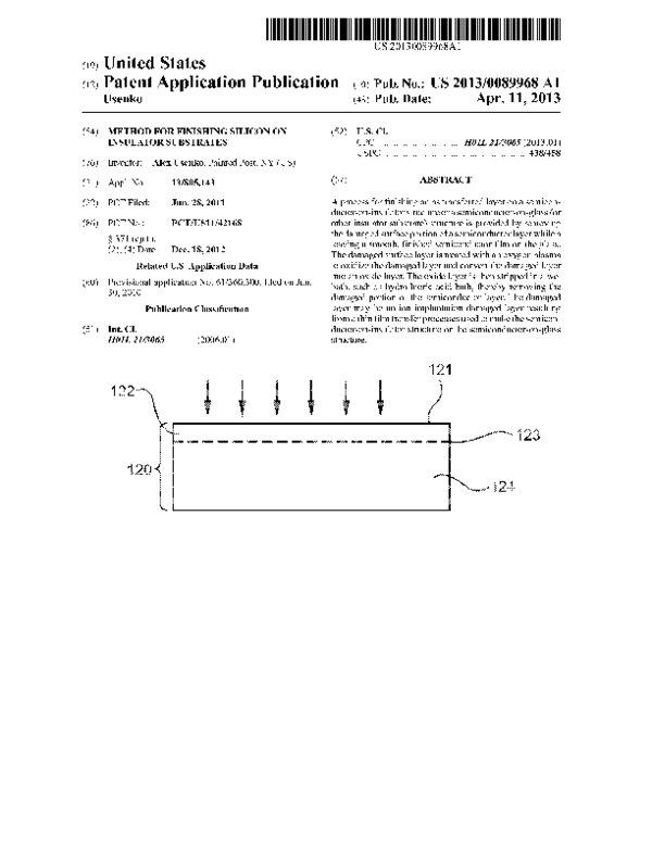
 Alex Usenko