JP7554208B2 - Method and mold for providing a MEMS device including pyramidal protrusions - Google Patents
Method and mold for providing a MEMS device including pyramidal protrusions Download PDFInfo
- Publication number
- JP7554208B2 JP7554208B2 JP2021560709A JP2021560709A JP7554208B2 JP 7554208 B2 JP7554208 B2 JP 7554208B2 JP 2021560709 A JP2021560709 A JP 2021560709A JP 2021560709 A JP2021560709 A JP 2021560709A JP 7554208 B2 JP7554208 B2 JP 7554208B2
- Authority
- JP
- Japan
- Prior art keywords
- layer
- silicon
- mold
- base substrate
- pit
- Prior art date
- Legal status (The legal status is an assumption and is not a legal conclusion. Google has not performed a legal analysis and makes no representation as to the accuracy of the status listed.)
- Active
Links
- 238000000034 method Methods 0.000 title claims description 59
- 239000000758 substrate Substances 0.000 claims description 54
- 239000000463 material Substances 0.000 claims description 41
- XUIMIQQOPSSXEZ-UHFFFAOYSA-N Silicon Chemical compound [Si] XUIMIQQOPSSXEZ-UHFFFAOYSA-N 0.000 claims description 38
- 239000000523 sample Substances 0.000 claims description 38
- 229910052710 silicon Inorganic materials 0.000 claims description 38
- 239000010703 silicon Substances 0.000 claims description 38
- 238000005530 etching Methods 0.000 claims description 37
- 238000004519 manufacturing process Methods 0.000 claims description 32
- 229910021420 polycrystalline silicon Inorganic materials 0.000 claims description 23
- 239000013067 intermediate product Substances 0.000 claims description 19
- VYPSYNLAJGMNEJ-UHFFFAOYSA-N Silicium dioxide Chemical compound O=[Si]=O VYPSYNLAJGMNEJ-UHFFFAOYSA-N 0.000 claims description 17
- 229910052814 silicon oxide Inorganic materials 0.000 claims description 17
- 238000000465 moulding Methods 0.000 claims description 16
- 230000000873 masking effect Effects 0.000 claims description 15
- 229910052581 Si3N4 Inorganic materials 0.000 claims description 12
- HQVNEWCFYHHQES-UHFFFAOYSA-N silicon nitride Chemical compound N12[Si]34N5[Si]62N3[Si]51N64 HQVNEWCFYHHQES-UHFFFAOYSA-N 0.000 claims description 12
- 229910021421 monocrystalline silicon Inorganic materials 0.000 claims description 10
- 229910003460 diamond Inorganic materials 0.000 claims description 5
- 239000010432 diamond Substances 0.000 claims description 5
- 238000000059 patterning Methods 0.000 claims description 5
- 229910021417 amorphous silicon Inorganic materials 0.000 claims description 4
- 238000000926 separation method Methods 0.000 claims description 3
- 229920005591 polysilicon Polymers 0.000 description 17
- KWYUFKZDYYNOTN-UHFFFAOYSA-M Potassium hydroxide Chemical compound [OH-].[K+] KWYUFKZDYYNOTN-UHFFFAOYSA-M 0.000 description 16
- 235000012431 wafers Nutrition 0.000 description 15
- 238000007493 shaping process Methods 0.000 description 11
- 238000000151 deposition Methods 0.000 description 9
- WGTYBPLFGIVFAS-UHFFFAOYSA-M tetramethylammonium hydroxide Chemical compound [OH-].C[N+](C)(C)C WGTYBPLFGIVFAS-UHFFFAOYSA-M 0.000 description 8
- 239000013078 crystal Substances 0.000 description 7
- 238000004518 low pressure chemical vapour deposition Methods 0.000 description 7
- 230000008021 deposition Effects 0.000 description 6
- 239000011888 foil Substances 0.000 description 6
- 230000003647 oxidation Effects 0.000 description 6
- 238000007254 oxidation reaction Methods 0.000 description 6
- 238000001020 plasma etching Methods 0.000 description 5
- KRHYYFGTRYWZRS-UHFFFAOYSA-N Fluorane Chemical compound F KRHYYFGTRYWZRS-UHFFFAOYSA-N 0.000 description 4
- 238000000708 deep reactive-ion etching Methods 0.000 description 4
- 229910052751 metal Inorganic materials 0.000 description 4
- 239000002184 metal Substances 0.000 description 4
- 238000001039 wet etching Methods 0.000 description 4
- BOTDANWDWHJENH-UHFFFAOYSA-N Tetraethyl orthosilicate Chemical compound CCO[Si](OCC)(OCC)OCC BOTDANWDWHJENH-UHFFFAOYSA-N 0.000 description 3
- 239000011521 glass Substances 0.000 description 3
- 238000004621 scanning probe microscopy Methods 0.000 description 3
- 229910004298 SiO 2 Inorganic materials 0.000 description 2
- 238000001312 dry etching Methods 0.000 description 2
- 239000010931 gold Substances 0.000 description 2
- 239000000126 substance Substances 0.000 description 2
- 230000002411 adverse Effects 0.000 description 1
- 238000000347 anisotropic wet etching Methods 0.000 description 1
- 239000011248 coating agent Substances 0.000 description 1
- 238000000576 coating method Methods 0.000 description 1
- 238000002508 contact lithography Methods 0.000 description 1
- 238000005516 engineering process Methods 0.000 description 1
- 230000002349 favourable effect Effects 0.000 description 1
- PCHJSUWPFVWCPO-UHFFFAOYSA-N gold Chemical compound [Au] PCHJSUWPFVWCPO-UHFFFAOYSA-N 0.000 description 1
- 229910052737 gold Inorganic materials 0.000 description 1
- 238000003384 imaging method Methods 0.000 description 1
- 238000007373 indentation Methods 0.000 description 1
- 238000001459 lithography Methods 0.000 description 1
- 238000005259 measurement Methods 0.000 description 1
- 238000005459 micromachining Methods 0.000 description 1
- 229920000642 polymer Polymers 0.000 description 1
- 239000000047 product Substances 0.000 description 1
- 239000004065 semiconductor Substances 0.000 description 1
- 239000007858 starting material Substances 0.000 description 1
- 238000003860 storage Methods 0.000 description 1
- 239000010409 thin film Substances 0.000 description 1
- 230000005641 tunneling Effects 0.000 description 1
- 238000009279 wet oxidation reaction Methods 0.000 description 1
Images


Classifications
-
- G—PHYSICS
- G01—MEASURING; TESTING
- G01Q—SCANNING-PROBE TECHNIQUES OR APPARATUS; APPLICATIONS OF SCANNING-PROBE TECHNIQUES, e.g. SCANNING PROBE MICROSCOPY [SPM]
- G01Q70/00—General aspects of SPM probes, their manufacture or their related instrumentation, insofar as they are not specially adapted to a single SPM technique covered by group G01Q60/00
- G01Q70/08—Probe characteristics
- G01Q70/10—Shape or taper
-
- G—PHYSICS
- G01—MEASURING; TESTING
- G01Q—SCANNING-PROBE TECHNIQUES OR APPARATUS; APPLICATIONS OF SCANNING-PROBE TECHNIQUES, e.g. SCANNING PROBE MICROSCOPY [SPM]
- G01Q70/00—General aspects of SPM probes, their manufacture or their related instrumentation, insofar as they are not specially adapted to a single SPM technique covered by group G01Q60/00
- G01Q70/16—Probe manufacture
-
- B—PERFORMING OPERATIONS; TRANSPORTING
- B81—MICROSTRUCTURAL TECHNOLOGY
- B81B—MICROSTRUCTURAL DEVICES OR SYSTEMS, e.g. MICROMECHANICAL DEVICES
- B81B2201/00—Specific applications of microelectromechanical systems
- B81B2201/12—STM or AFM microtips
Landscapes
- Physics & Mathematics (AREA)
- Health & Medical Sciences (AREA)
- General Health & Medical Sciences (AREA)
- General Physics & Mathematics (AREA)
- Nuclear Medicine, Radiotherapy & Molecular Imaging (AREA)
- Radiology & Medical Imaging (AREA)
- Micromachines (AREA)
Description
本発明は、多数のMEMS方法ステップを使用して、三角錐状突起を含むMEMSデバイスを提供する方法に関する。 The present invention relates to a method for providing a MEMS device including triangular pyramidal protrusions using multiple MEMS method steps.
当該技術分野では、突起を含むMEMSデバイスを製造する方法が知られている。この典型例は、プローブ、例えば走査に使用されるプローブである。近頃では、そのようなプローブは、基材として<100>シリコンウエハを用い、異方性エッチングを使用して、大量生産される。 Methods are known in the art for manufacturing MEMS devices that include protrusions. A typical example of this is a probe, for example a probe used for scanning. Nowadays, such probes are mass-produced using <100> silicon wafers as substrate and anisotropic etching.
概して、ピラミッド状チップを製造するために、2つの方法が認められ得る:
1)シリコンエッチングによってチップを生じるシリコンチップの製造。
2)走査型プローブ顕微鏡法(SPM:scanning probe microscopy)電界エミッター、真空エレクトロニクス、又はトンネリングベースのデバイスで使用されるもののような、非常に鋭いチップを生産するための、周知のナノファブリケーション方法であるチップ成形。チップ成形は、犠牲基板(一般にシリコン)にピラミッド状のピットをエッチングすること、型に所望の薄膜材料を堆積すること、堆積した材料に、片持ちアームなどの他の特徴を画成するようにさらに処理すること、その後、犠牲基板を除去して、ピラミッド状のチップの姿を見せるようにすることからなる。最も一般的な型の幾何学的形状は、<100>Siウエハが異方性エッチングによってエッチングされて得られる方錐(四角錐)である。
Generally, two methods can be recognized for producing pyramidal tips:
1) Silicon chip manufacturing, where the chips are produced by silicon etching.
2) Tip molding, a well-known nanofabrication method for producing very sharp tips, such as those used in scanning probe microscopy (SPM) field emitters, vacuum electronics, or tunneling-based devices. Tip molding consists of etching pyramidal pits in a sacrificial substrate (typically silicon), depositing the desired thin-film material on the mold, further processing the deposited material to define other features such as cantilever arms, and then removing the sacrificial substrate to reveal the pyramidal tip. The most common mold geometry is a square pyramid, obtained by anisotropically etching a <100> Si wafer.
チップ成形技術にはいくつかの利点がある:
1)チップ材料は、用途に応じて選択できる。材料は、シリコンよりも硬質に/より耐摩耗性を高くできる。チップ材料はまた、シリコンとは異なる誘電特性を有してもよい。チップ材料は、例えば、窒化ケイ素、ダイアモンド、金属又はポリマーとし得る。
2)片持ち梁特性は、より良好に制御できる。それらは、剛性がより正確に定義された、より小さい及び/又はより軟質の片持ち梁とし得る(成形プローブの厚さは、エッチングによるよりも堆積による方が、簡単に制御できるため)。
3)いずれの能動構成要素も、MEMSデバイス(プローブ)に簡単に組み込まれる。そのような能動構成要素の例は、ヒータ、センサー、及びアクチュエータである。
Chip forming technology has several advantages:
1) The tip material can be chosen depending on the application. The material can be harder/more wear resistant than silicon. The tip material may also have different dielectric properties than silicon. The tip material can be, for example, silicon nitride, diamond, metal or polymer.
2) The cantilever properties can be better controlled: they can be smaller and/or softer cantilevers with more precisely defined stiffness (because the thickness of the shaped probes can be more easily controlled by deposition than by etching).
3) Any active components are easily integrated into the MEMS device (probe). Examples of such active components are heaters, sensors, and actuators.
公知の方法の欠点は、4つの平面を含むピラミッド形状の、結果として生じる突起が、1つの先端を有するのではなく、2つの先端か(それぞれ3つの平面によって形成される)又は1つのリッジを有することである。換言すると、ピラミッド状チップは、先端が1つのみであった場合ほどには鋭くない。これは、3つの<111>平面によって画成されたピットを形成するために、Si(311)ウエハをエッチングすることによって三面チップを製造することについて開示している論文“Advances in Manufacturing of Molded Tips for Scanning Probe Microscopy”([2012] N. Moldovan et al in JOURNAL OF MICROELECTROMECHANICAL SYSTEMS, VOL. 21, NO. 2, APRIL 2012では、楔と呼ばれている。この方法を使用して生産されたチップは比較的大きい円錐角を有し、それらのチップを、AFMプローブなどの走査目的にはあまり適さないものにする。この問題は、“Advanced Micromachining Schemed for Scanning Probe Tips”(PhD Thesis Rolf Vermeer [2016])において、及び論文“Fabrication of novel AFM probe with High-Aspect-Ratio Ultra-Sharp Three-Face Silicon Nitride Tips”(R. Vermeer et al in 14TH IEEE INTERNATIONAL CONFERENCE ON NANOTECHNOLOGY, IEEE, 18 August 2014, pages 229-233, XP032690978, 001: 10.11 09/NANO.2014.6967957)から、取り組まれており、これは、プローブ用の三角錐チップの製造のために<111>シリコンを使用することを開示している。このプロセスは、基材を除去するためにドライエッチングを使用しているので、製造のコスト及び速度に悪影響を与える。 A disadvantage of the known method is that the resulting protrusion, in the shape of a pyramid containing four planes, has not one tip, but two tips (each formed by three planes) or one ridge. In other words, the pyramidal tip is not as sharp as it would be if there was only one tip. This is called a wedge in the paper “Advances in Manufacturing of Molded Tips for Scanning Probe Microscopy” ([2012] N. Moldovan et al in JOURNAL OF MICROELECTROMECHANICAL SYSTEMS, VOL. 21, NO. 2, APRIL 2012) which discloses the fabrication of three-sided tips by etching a Si(311) wafer to form a pit defined by three <111> planes. Tips produced using this method have a relatively large cone angle, making them less suitable for scanning purposes such as AFM probes. This problem is discussed in “Advanced Micromachining Schemed for Scanning Probe Tips” (PhD Thesis Rolf Vermeer [2016]) and in the paper “Fabrication of novel AFM probe with High-Aspect-Ratio Ultra-Sharp Three-Face Silicon Nitride Tips” (R. Vermeer et al in 14TH IEEE INTERNATIONAL CONFERENCE ON NANOTECHNOLOGY, IEEE, 18 August 2014, pages 229-233, XP032690978, 001: 10.11 09/NANO.2014.6967957), which discloses the use of <111> silicon for the fabrication of triangular pyramidal tips for probes. This process uses dry etching to remove the substrate, which adversely affects the cost and speed of fabrication.
本発明の目的は、三面突起を含むMEMSデバイスの信頼性高く且つ迅速な製造を大規模で可能にする方法を提供することにあり、突起は、比較的小さいハーフコーンアングル(half-cone angle)及び単一の先端を有する。 The object of the present invention is to provide a method that allows for reliable and rapid large-scale manufacturing of MEMS devices that include three-sided protrusions, the protrusions having a relatively small half-cone angle and a single tip.
この目的に向けて、前文による方法は、型が使用され、前記型は、
- 第1の側面及び第2の側面を画成し、
- ベース基板を含み、型の第1の側面では、ベース基板の表面が、第1の側面と平行な主平面を画成し、前記主平面が、単結晶シリコンの<111>平面を画成し、
- 型の第1の側面において、ベース基板の上部に犠牲層を含み、前記犠牲層は、多結晶シリコン及び非晶質シリコンから選択され;
- 型の第1の側面にピットを含み、前記ピットは、
- 犠牲層を通って[出願時の本出願のpage 3 lines 18-19]ベース基板内へと延在し、及び
- <111>結晶面と平行な3つの壁部分を含み、3つの壁部分のそれぞれは、他の2つの壁部分と交差し、及び
- ピットの底部分の頂点を含み;
MEMSデバイスを提供する方法は、
- 型の第1の側面において、ピット外の第1の副区域から、ピットの頂点を含む第2の副区域まで延在する区域に、突起材料の層を提供すること、
- 突起材料の層を所望の形状にパターニングすること、及び
- MEMSデバイスを少なくとも型のベース基板から分離するために、犠牲層をエッチングできる等方性エッチャントによって、型の犠牲層を等方的にエッチングすること
を含むことを特徴とする。
To this end, the method according to the preamble uses a mold, said mold comprising:
- defining a first side and a second side;
- a base substrate, at a first side of the mold, the surface of the base substrate defines a main plane parallel to the first side, said main plane defining a <111> plane of monocrystalline silicon;
- in a first aspect of the mold, a sacrificial layer on top of a base substrate, said sacrificial layer being selected from polycrystalline silicon and amorphous silicon;
- a pit in a first side of the mould, said pit comprising:
- extending through the sacrificial layer [page 3 lines 18-19 of this application as filed] into the base substrate, and - including three wall portions parallel to the <111> crystal planes, each of the three wall portions intersecting the other two wall portions, and - including an apex at the bottom of the pit;
A method of providing a MEMS device includes:
providing a layer of protruding material on a first side of the mould in an area extending from a first sub-area outside the pits to a second sub-area including the apex of the pits;
- patterning a layer of protruding material into a desired shape; and - isotropically etching a sacrificial layer of the mold by an isotropic etchant capable of etching the sacrificial layer, in order to separate the MEMS device from at least the base substrate of the mold.
それゆえ、鋭い先端を含む突起を含むMEMSデバイスが生産され得る。ベース基板は、突起を含む多数のMEMSデバイスを好都合に生産するために使用され得る。 Therefore, MEMS devices can be produced that include protrusions that include sharp tips. The base substrate can be used to conveniently produce a large number of MEMS devices that include protrusions.
本方法の別の利点は、シリコン基材全体を溶解することなくデバイスを得ることができることであり、シリコン基材全体の溶解は、<111>方位のシリコンであることを考えると、幾分時間がかかる。 Another advantage of this method is that the device can be obtained without dissolving the entire silicon substrate, which takes some time given the <111> orientation of the silicon.
典型的な方法は、MEMSデバイスを最終加工するためのさらなるステップを含む。 Typical methods include further steps for final processing of the MEMS device.
ピットは、第1から犠牲層を通ってベース基板まで延在する。 The pits extend from the first through the sacrificial layer to the base substrate.
プローブを含む大容量記憶デバイスの製作方法が、米国特許出願公開第2006/003493A1号から知られており、ここでは、プローブは、基板に動作可能に接続された第1の端部領域と、第1の端部領域の反対側になるような方向に回転される第2の端部領域とを有する、片持ち梁を有する。第2の端部領域にはチップが配置され、チップは、第1の端部領域とは反対側の方向を指している。 A method for fabricating a mass storage device including a probe is known from US 2006/003493 A1, in which the probe has a cantilever having a first end region operably connected to a substrate and a second end region rotated in an orientation opposite the first end region. A tip is disposed at the second end region, the tip pointing in a direction opposite the first end region.
鋭いチップを生産する方法が、米国特許第8701211B2号から知られている。チップは、3面の、1つ又は複数の三面体若しくは三角錐状型、又は1つ若しくは複数の刻み目を形成するために結晶エッチャントによってエッチングされている、露出{311}面を備える犠牲結晶性半導体基板に形成された1つ又は複数の型に堆積することによって、形成される。 A method for producing sharp tips is known from US Pat. No. 8,701,211 B2. The tips are formed by depositing on one or more three-sided trihedral or pyramidal tips or tips formed on a sacrificial crystalline semiconductor substrate with exposed {311} faces that are etched by a crystal etchant to form one or more indentations.
好都合な実施形態によれば、型は、中間生成物に複数の方法ステップを受けさせて型を形成することによって準備され、中間生成物は、
- 第1の側面及び第2の側面を画成し、及び
- ベース基板を含み、中間生成物の第1の側面では、ベース基板の表面が、第1の側面と平行な主平面を画成し、前記主平面が、単結晶シリコンの<111>平面を画成し;
複数の方法ステップは、
- 第1の側面において、中間生成物のベース基板に第1の材料の犠牲層を提供するステップであって、前記第1の材料は非単結晶シリコンであるステップ、
- 中間生成物の犠牲層に、第1の材料とは異なる第2の材料のマスキング層を提供するステップ、
- 中間生成物に、第1の側面からベース基板内へと延在する止まり穴を提供するステップ、
- 中間生成物に、シリコン基材層の<111>結晶面の異方性エッチングの速度と少なくとも同じ速度で、主平面に対して平行ないずれの方向においても犠牲層をエッチングできるエッチャントを使用して、シリコンの異方性エッチングを受けさせるステップであって、3つのピラミッド状の壁部分を含むピットを形成するようにするステップ、
- 第2の材料のマスキング層を除去するステップ、
- 中間生成物のピットに、成形層を提供するステップであって、成形層は、型を形成するために、3つの壁部分によってピットの頂点を形成するステップ
を含む。
According to an advantageous embodiment, the mould is prepared by subjecting an intermediate product to a number of method steps to form the mould, the intermediate product comprising:
- defining a first side and a second side; and - comprising a base substrate, wherein at the first side of the intermediate product, a surface of the base substrate defines a major plane parallel to the first side, said major plane defining a <111> plane of monocrystalline silicon;
The method steps include:
- in a first aspect, providing a sacrificial layer of a first material on the base substrate of the intermediate product, said first material being non-monocrystalline silicon;
providing the sacrificial layer of the intermediate product with a masking layer of a second material different from the first material;
- providing the intermediate product with a blind hole extending from a first side into the base substrate;
- subjecting the intermediate product to anisotropic etching of silicon using an etchant capable of etching the sacrificial layer in any direction parallel to the main surface at least as fast as the rate of anisotropic etching of the <111> crystal planes of the silicon substrate layer, so as to form pits comprising three pyramidal wall portions;
- removing the masking layer of the second material;
providing a shaping layer in the pit of the intermediate product, the shaping layer comprising a vertex of the pit formed by three wall portions to form a mould;
低圧化学蒸着(LPCVD:Low Pressure Chemical Vapor Deposition)は、犠牲層として多結晶シリコンの層を堆積するために使用され得る。これは、多結晶シリコン及び<111>シリコン基材をエッチングするためのTMAH又はKOHなどの異方性エッチャントによって、等方的にエッチングされる。 Low Pressure Chemical Vapor Deposition (LPCVD) can be used to deposit a layer of polysilicon as a sacrificial layer. This is isotropically etched with anisotropic etchants such as TMAH or KOH to etch polysilicon and <111> silicon substrates.
ピットに成形層を提供するステップは、成形層を堆積すること、又は成形層を成長させることを含み得る。 The step of providing the shaped layer in the pit may include depositing the shaped layer or growing the shaped layer.
一般に、マスキング層は、成形層を提供するステップの前に除去される。 Typically, the masking layer is removed prior to the step of providing the molding layer.
止まり穴を形成するために、開口部、一般に円形開口部がマスキング層に作られ得る。その後、止まり穴が、複数層スタック(例えば酸化ケイ素、多結晶シリコン及び単結晶シリコン)の方向性エッチングによって、例えば反応性イオンエッチング(RIE:Reactive Ion Etching)及びディープ反応性イオンエッチング(DRIE:Deep Reactive Ion Etching)と組み合わせて作られて、主平面に直角の壁のある止まり穴を得ることができる。止まり穴の深さは、後で突起の高さを決定する。 To form the blind hole, an opening, typically a circular opening, can be made in the masking layer. The blind hole is then made by directional etching of the multilayer stack (e.g. silicon oxide, polycrystalline silicon and monocrystalline silicon), e.g. in combination with reactive ion etching (RIE) and deep reactive ion etching (DRIE) to obtain a blind hole with walls perpendicular to the main plane. The depth of the blind hole determines the height of the protrusion later.
基材からMEMSデバイスを分離する際に成形層が除去されていない場合、このステップは、単一の先端を有する突起を含むMEMSデバイスを生じるように、実施される。 If the molding layer is not removed when separating the MEMS device from the substrate, this step is performed to yield a MEMS device that includes a protrusion having a single tip.
成形層は、一般に、比較的薄く(例えば1um)、且つ大きな表面領域が露出されているため、ここは、非常に時間のかかる<111>平面に沿ったエッチングを必要とするVermeerの方法(上記)における基材の除去と比べて、比較的迅速に行われ得る。 Because the shaping layer is generally relatively thin (e.g., 1 um) and has a large surface area exposed, this can be accomplished relatively quickly compared to the substrate removal in the Vermeer method (mentioned above), which requires etching along the <111> planes, which is very time consuming.
成形層として、酸化ケイ素の場合、好都合なことに、ウェットエッチングによって除去される。好適なエッチャントはバッファードフッ酸(BHF:Buffered HydroFluoric acid)である。 In the case of silicon oxide as the molding layer, it is conveniently removed by wet etching. A suitable etchant is buffered hydrofluoric acid (BHF).
好都合な実施形態によれば、成形層を提供するステップは、成形層を成長させることを含む。 According to an advantageous embodiment, the step of providing the shaped layer includes growing the shaped layer.
これは、最終的な突起の先端を非常に鋭く画成するのを支援する。 This helps define the tip of the final projection very sharply.
成形層は、酸化ケイ素を含み得、これは、シリコンベースの犠牲層及び<111>シリコンから簡単に成長する。 The shaping layer can include silicon oxide, which is easily grown from silicon-based sacrificial layers and <111> silicon.
好都合な実施形態によれば、中間生成物に、主平面に対して平行ないずれの方向においても犠牲層をエッチングできるエッチャントを使用して、シリコンの異方性エッチングを受けさせるステップは、ピットを形成するために、<111>シリコン基材層の異方性エッチングの速度よりも速い速度で、エッチングすることを含む。 According to an advantageous embodiment, the step of subjecting the intermediate product to anisotropic etching of silicon using an etchant capable of etching the sacrificial layer in any direction parallel to the major surface includes etching at a rate faster than the rate of anisotropic etching of the <111> silicon substrate layer to form pits.
形成されたピットは、ピラミッド状チップ壁部分によって画成された平面を越えて(平面外へ)延在するチップ底面部分を含む。換言すると、比較的広いチップ底面部分が形成され、これは、チップの強度に関して好都合である。 The pits formed include chip bottom portions that extend beyond (out of) the plane defined by the pyramidal chip wall portions. In other words, a relatively wide chip bottom portion is formed, which is favorable with respect to chip strength.
好都合な実施形態によれば、MEMSデバイスと型の分離後、成形層は、エッチングによって除去される。 According to an advantageous embodiment, after separation of the MEMS device and the mold, the molding layer is removed by etching.
成形層は、一般に、比較的薄く(例えば1um)、大きな表面領域が露出されているため、ここは、Vermeerの方法(上記)における(111)の除去と比較して、比較的迅速に行われ得る。 The shaping layer is generally relatively thin (e.g., 1 um) and has a large surface area exposed, so this can be done relatively quickly compared to removing (111) in the Vermeer method (above).
成形層として、酸化ケイ素の場合、ウェットエッチングによって好都合に除去される。好適なエッチャントはバッファードフッ酸(BHF)である。 In the case of silicon oxide as the molding layer, it is conveniently removed by wet etching. A suitable etchant is buffered hydrofluoric acid (BHF).
好都合な実施形態によれば、マスキング層は、i)窒化ケイ素、及びii)酸化ケイ素から選択される。 According to an advantageous embodiment, the masking layer is selected from i) silicon nitride, and ii) silicon oxide.
成形層は酸化ケイ素であり、及び突起材料は窒化ケイ素であることが好ましい。そのようなマスキング層は、バッファードHF(BHF)によって簡単に除去され得るが、犠牲層及びシリコン基材を残す。 The molding layer is preferably silicon oxide and the protrusion material is silicon nitride. Such a masking layer can be easily removed with buffered HF (BHF), leaving behind the sacrificial layer and the silicon substrate.
好都合な実施形態によれば、突起材料の層は、i)窒化ケイ素、及びii)ダイアモンドから選択される材料を含む。 According to an advantageous embodiment, the layer of protrusion material comprises a material selected from i) silicon nitride, and ii) diamond.
これらは、鋭くて耐摩耗性の突起を作るのに優れた硬質材料である。 These are hard materials that are excellent for making sharp, wear-resistant protrusions.
好都合な実施形態によれば、突起材料の層は、副層のスタックとして形成され、方法は、第1の突起材料の第1の副層を提供すること、それに続いて、第1の突起材料とは異なる第2の突起材料の第2の副層を提供することを含む。 According to an advantageous embodiment, the layer of protrusion material is formed as a stack of sublayers, and the method includes providing a first sublayer of a first protrusion material, followed by providing a second sublayer of a second protrusion material different from the first protrusion material.
それゆえ、突起の特性は、MEMSデバイスに対する特定の要件に合わせられ得る。第1の副層は、例えば、耐摩耗性の層を提供するためにダイアモンドとしてもよい。第1の副層はまた、導電層を提供するために金属としてもよい。 The properties of the protrusions can therefore be tailored to the specific requirements for the MEMS device. The first sublayer may, for example, be diamond to provide a wear-resistant layer. The first sublayer may also be metal to provide a conductive layer.
第2の材料は、例えば、第1の材料によっては得られない所望の機械的特性を備えた、MEMSプローブのチップ及び片持ち梁を提供するために、窒化ケイ素としてもよい。 The second material may be, for example, silicon nitride to provide the tip and cantilever of the MEMS probe with desired mechanical properties not available from the first material.
好都合な実施形態によれば、MEMSデバイスはプローブである。 According to an advantageous embodiment, the MEMS device is a probe.
これは、本発明の方法には非常に重要な応用分野である。突起の鋭い先端は、より正確な測定を可能にする。 This is a very important application area for the method of the present invention. The sharp tip of the protrusion allows for more accurate measurements.
最後に、本発明は、MEMSデバイスを製造するための型に関し;
前記型は、
- 第1の側面及び第2の側面を画成し、
- ベース基板を含み、型の第1の側面では、ベース基板の表面が、第1の側面と平行な主平面を画成し、前記主平面が、単結晶シリコンの<111>平面を画成し、
- 型の第1の側面では、ベース基板の上部に犠牲層を含み、前記犠牲層は、多結晶シリコン及び非晶質シリコンから選択され、
及び
- 型の第1の側面にピットを含み、前記ピットは、
- 犠牲層を通ってベース基板内へと延在し、及び
- <111>結晶面と平行な3つの壁部分を含み、3つの壁部分のそれぞれは、他の2つの壁部分と交差し、及び
- ピットの底部分の頂点を含む。
Finally, the invention relates to a mould for manufacturing a MEMS device;
The mold is
- defining a first side and a second side;
- a base substrate, at a first side of the mold, the surface of the base substrate defines a main plane parallel to the first side, said main plane defining a <111> plane of monocrystalline silicon;
In a first aspect of the mold, the mold includes a sacrificial layer on top of a base substrate, the sacrificial layer being selected from polycrystalline silicon and amorphous silicon;
and - a pit on the first side of the mold, said pit comprising:
- extends through the sacrificial layer into the base substrate; and - includes three wall portions parallel to the <111> crystal planes, each of the three wall portions intersecting the other two wall portions; and - includes an apex at the bottom of the pit.
そのような型は、本発明による方法に非常に有用である。一般に、ウエハは、複数の型を含み、且つ本発明による方法において使用され得る。 Such moulds are very useful in the method according to the invention. Generally, a wafer may contain multiple moulds and be used in the method according to the invention.
ピットは、第1から犠牲層を通ってベース基板内へ延在する。 The pits extend from the first through the sacrificial layer into the base substrate.
好都合な実施形態によれば、犠牲層は、成形層によって少なくとも部分的に覆われ、成形層は、ピットの頂点を形成する。 According to an advantageous embodiment, the sacrificial layer is at least partially covered by a molding layer, which forms the apex of the pit.
そのため、形成されるべきチップの形状は、正に犠牲層のみで可能であるよりも大幅に制御され得、及び/又は犠牲層は、分離速度に関してより選択され得、且つ成形層は、チップの形状をより良好に制御するために選択され得る。 Thus, the shape of the chip to be formed can be controlled to a greater extent than is possible with just the sacrificial layer alone, and/or the sacrificial layer can be more selective with respect to separation speed and the molding layer can be selected to better control the shape of the chip.
本発明を、ここで、図面を参照して説明する。 The present invention will now be described with reference to the drawings.
図1は、MEMSデバイス100の断面図を示し、ここで、プローブ100は、プローブ本体110と、近位端121及び遠位端122のある片持ち梁120と、遠位端部分に、チップユニット130とを含む。
Figure 1 shows a cross-sectional view of a
チップユニット130は、チップ底面131と、先端133を備えるピラミッド状チップ132とを含む。ピラミッド状チップ132は、四面体チップ132である、すなわち先端133で接する3つの側面を有する。ハーフコーンアングルは20°である。
The
本発明による方法を、ここで、図2A~図2Nを使用して説明し、ここで、各図面は、ステップを、上面図及び断面図の双方で示す。方法ステップは、図1のプローブ100の製造を例示する。
The method according to the invention will now be described using Figures 2A-2N, where each figure shows steps in both top and cross-sectional views. The method steps illustrate the manufacture of the
製作プロセスは、出発原料として<111>シリコンウエハ210(図2A)を使用して、型200の製造から始まる。型200が完成するまで、型の半生成物を、中間生成物200’と呼ぶ。ウエハ210は、第1の主側面211及び第2の主側面212を含む。
The fabrication process begins with the fabrication of
ウエハ210上には、低圧化学蒸着(LPCVD)を使用して、厚さ1umの多結晶シリコン(ポリシリコン)犠牲層220が堆積される(図2B)。
A 1 um thick polycrystalline silicon (polysilicon)
概して、ポリシリコン層の厚さが選択されるとき、成形層が堆積される方法が考慮される必要がある。成形層(酸化ケイ素)が熱成長すると、ポリシリコン層は、熱酸化プロセス中に壊されて(consumed)しまう。ポリシリコン層は、熱酸化後に、ポリシリコン層の一部がウエハ上に残るように、十分に厚い必要がある。現実的なアプローチは、1umのポリシリコンで始まり、且つ熱酸化による約1um厚さの酸化ケイ素層の成長後、約500nm厚さのポリシリコンがウエハに残ることである。その後、この残っている層を、MEMSプローブ放出のための犠牲層として使用する。 In general, when the thickness of the polysilicon layer is selected, the way in which the shaping layer is deposited needs to be considered. If the shaping layer (silicon oxide) is thermally grown, the polysilicon layer will be consumed during the thermal oxidation process. The polysilicon layer needs to be thick enough so that after thermal oxidation, a portion of the polysilicon layer remains on the wafer. A practical approach is to start with 1 um of polysilicon, and after growth of a silicon oxide layer about 1 um thick by thermal oxidation, about 500 nm of polysilicon remains on the wafer. This remaining layer is then used as a sacrificial layer for the MEMS probe release.
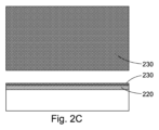
続いて、マスキング層230が堆積される(図2C)。この層は、後で、シリコンの異方性ウェットエッチング中に、ポリシリコン層を保護する働きをする。この実施形態では、酸化ケイ素は、高温熱酸化(15分間の1000℃でのウェット酸化、約150nmのSiO2層を生じる)を使用してポリシリコン犠牲層220上で成長されたマスキング層として使用される。代替的な方法は、SiO2を堆積するために、LPCVD堆積を使用することである。別のオプションは、マスキング層として窒化ケイ素を使用することである。酸化ケイ素及び窒化ケイ素は双方とも、後で、シリコンの異方性エッチング(例えばKOH又はTMAHによる)に使用される化学エッチャントに対して、安定したマスキング材料である。
A
標準的なリソグラフィー技術(図示せず)による円形開口部のパターニング後、反応性イオンエッチング(RIE)とディープ反応性イオンエッチング(DRIE)の組み合わせを使用して、複数層スタックの方向性エッチングによって、シリンダー状穴235が作られる(図2D)。シリンダー状ピット235の寸法(及び下記で説明する成形層240の厚さ)は、チップユニット130の高さ(片持ち梁120から先端133まで)を決定する要因である。シリンダー状ピット235の底部は、ピラミッド状チップ132の三角形の底面の正三角形の辺長を決定する要因である。ピット235のシリコンの異方性エッチング中、ピラミッド状チップ132の三角形の辺は、最も遠い<111>平面に到達するときに、決定される。3つの側面全てでこれが発生すると、正三角形がチップ底面131に形成される。それは、ピット235の形状が、正三角形を得るために完全にシリンダー状である必要はないことを意味する。<111>平面間の角度は、単結晶シリコン基材の結晶構造によって決定される。シリコンの<111>平面はまた、異方性エッチャントでエッチングされ(平面の他の迅速なエッチングよりも遥かにゆっくりではあるが)、そのため、三角形の底面の辺の最終的な長さは、シリンダー状ピットの初期形状によって決まるだけでなく、異方性エッチング時間によっても決まる。
After patterning the circular opening by standard lithography techniques (not shown), a
シリンダー状ピット235の方向性エッチング後、ウエハは、水酸化カリウム(KOH)に浸された。KOHは、ポリシリコンを同位体的に(topically)、すなわち全ての方向において同じエッチ速度で、エッチングする。他方では、基材層110の<111>シリコンは、非同位体的に(anisotopically)エッチングされる。その場合には、<111>平面は、他の結晶平面よりも遥かにゆっくりとエッチングされる。このようにして、四面体チップユニット型250が形成される(図2E)。
After the directional etching of the
チップユニット型250の底部分は、非常に滑らかな壁を有する四面体型部分250’である。四面体型のこの底部分は、正三角形である。
The bottom portion of the
ポリシリコン犠牲層と<111>シリコンの同時エッチングは、チップユニット型250の最上部分をより幅広にする。その理由は、ポリシリコンのエッチ速度が速いため、(111)結晶面にエッチング速度が追い付かない、第1の側面から、基材の<111>シリコンのエッチングを可能にするからである。
Simultaneous etching of the polysilicon sacrificial layer and the <111> silicon makes the top portion of the
シリコンの他の異方性エッチャントは、型を形成するために使用され得る(例えばTMAH)。 Other anisotropic etchants for silicon can be used to form the mold (e.g. TMAH).
KOHエッチングの期間中にポリシリコン層220を保護したマスキング層230の酸化ケイ素は、高濃度のHF(50%HF)を使用して除去され、ポリシリコン及び<111>シリコン基材を残す。
The silicon oxide of the
次いで、酸化ケイ素成形層240が、堆積によって、成長されることによって、又はそれら双方によって、共形的に(すなわち、水平面部分上又は傾斜面部分上にあるかどうかに関わらず、同じ厚さを有する)提供される(図2G)。酸化ケイ素層は、LPCVDによって堆積され得るか(オルトケイ酸テトラエチルから堆積された酸化ケイ素、いわゆるTEOS堆積)、又は熱酸化によって成長され得る。TEOS堆積と熱酸化の組み合わせも使用できる。成形に関するより多くの情報は、VermeerのPhD論文(上記のchapter 3.3参照)に見出され得る。酸化ケイ素層は、底のチップユニット型部分250’の底を完全に補充し、チップユニット型の頂点251’が形成されるように、十分に厚い必要があり、それにより、鋭いAFMチップ132を得ることができるようにする。ここで型200は、MEMSデバイスの製造準備が整う。
Then, a silicon
鋭いピットを備えるチップユニット型250を含む型200が作られた後、突起材料の構造層260が堆積され(図2H)、この実施形態では、窒化ケイ素がLPCVDによって厚さ600nmで堆積される。
After the
構造層がパターニングされて(図2I)、標準的なコンタクトリソグラフィをRIEと組み合わせて使用して、片持ち梁120及び片持ち梁基部271を作り出す。
The structural layer is patterned (FIG. 2I) using standard contact lithography in combination with RIE to create the
パターニング後、シリコンウエハは、陽極ボンディングによって予備的にさいの目に切り込みが入れられたガラスウエハ280にボンディングされる(図2J)。
After patterning, the silicon wafer is bonded to a
ここで、MEMSデバイスは、型200の基材から分離される(すなわち解放される)必要がある。
The MEMS device now needs to be separated (i.e., released) from the substrate of the
この目的に向けて、片持ち梁120及び片持ち梁基部271の真下にある犠牲ポリシリコン層220が、ウェット化学エッチングを使用して除去され(この実施形態では90℃で25重量%のTMAH)、これはまた、チップユニット130の周りのシリコンベース基板をエッチングする。このようにして、基材を完全にエッチングする必要なく、プローブ全体が基材から放出される-すなわち型200のほとんどが除去される(図2K)。これは時間を節約する、なぜなら、特に、ウェットエッチングによるか又はドライエッチングによるかに関わらず、<111>方位のシリコンはゆっくりとエッチングされるためである。500um厚さの(100)シリコンウエハを完全に溶解する-これは、四角錐状チップを有するMEMSデバイスの製造中に行われる-ためには、約8時間のウェットエッチングを要する。<111>シリコンウエハ材料の完全な除去は、100倍時間がかかり、それゆえ、800時間程度かかる。
To this end, the
放出されたMEMSデバイスは、それ自体当該技術分野で公知のように、ガラス基板がいくつかの方向において完全にさいの目に切られていないため(図示せず)、依然として一緒に接続されている。また、シリコンウエハのエッジは、型200の製造中にそこに犠牲シリコン層が堆積されなかったため、依然としてガラス基板と接続されている(図示せず)。
The released MEMS devices are still connected together because the glass substrate is not perfectly diced in some directions (not shown), as is known per se in the art. Also, the edges of the silicon wafer are still connected to the glass substrate (not shown), because no sacrificial silicon layer was deposited there during the manufacture of the
型200からのMEMSデバイスの放出後、バッファードHF(BHF)を使用して酸化ケイ素成形層240が除去される(図2L)。
After release of the MEMS device from the
この実施形態では、MEMSプローブは、金属層290の堆積によって金属化される(本出願人らは、反射コーティングとしてTi/Au二層を使用する。Ti層は、厚さ10nmの接着層である。金の反射層は50nm厚さである)。この金属層290は、AFM撮像用の片持ち梁120上の反射層の働きをする。
In this embodiment, the MEMS probe is metallized by deposition of a metal layer 290 (we use a Ti/Au bilayer as the reflective coating. The Ti layer is an adhesion layer with a thickness of 10 nm. The gold reflective layer is 50 nm thick). This
或いは、パターニングにより多くの加工ステップを費やすことで、プロセスの早期にそのような反射層を(窒化ケイ素構造層260の上部に)堆積することが可能である。いずれの場合も、副層のスタックが形成される。 Alternatively, such a reflective layer can be deposited earlier in the process (on top of the silicon nitride structural layer 260) by devoting more processing steps to patterning. In either case, a stack of sublayers is formed.
プロセスのさらに早期に副層を、例えば成形層240の上部の第1の副層として、堆積することも可能である。これは例えば、突起に、片持ち梁の構造材料とは異なる材料でコーティングされている先端を設ける必要がある場合に、例えばダイアモンドでコーティングされているチップを有することが望ましい場合に、行われる。
It is also possible to deposit a sublayer earlier in the process, for example as a first sublayer on top of shaping
ここで、MEMSデバイス100は使用準備が整い、且つダイシングによって取り外され得る。片持ち梁が折れるリスクを低下させるために、第1の主側面に粘着性のある箔(UVダイシング箔)を貼る公知の技術が使用される。箔を除去することによって、MEMSプローブが取り外される。このようにして、全MEMSプローブが箔へ移される。UV箔をUV光へ曝露することによって、箔の粘着性が低下される。曝露後、個々のMEMSプローブが、ピンセットを使用して、箔から集められ得る。
The
図3は、第1の主側面211から第2の主側面212の方へ向かって見るような、KOHエッチングによるマスキング層の除去後(図2F)の、チップユニット型250のチップユニット型部分250’の走査型電子顕微鏡の写真である。中心には、チップユニット型部分250’を画成する3つの<111>平面があり、且つその周りには、チップユニット型250のより幅広の最上部分がある。第1の主側面211では、チップユニット型250のより幅広の最上部分は、(実質的に)円形の外周を有している。
3 is a scanning electron microscope photograph of the chip unit mold portion 250' of the
Claims (11)
型(200)が使用され、前記型(200)は、
- 第1の側面(211)及び第2の側面(212)を画成し、
- ベース基板を含み、前記型の前記第1の側面(211)では、前記ベース基板の表面が、前記第1の側面(211)と平行な主平面を画成し、前記主平面が、単結晶シリコンの<111>平面を画成し、
- 前記型(200)の前記第1の側面において、前記ベース基板の上部に犠牲層(220)を含み、前記犠牲層(220)は、多結晶シリコン及び非晶質シリコンから選択され;
- 前記型(200)の前記第1の側面(211)にピット(235)を含み、前記ピット(235)は、
- 前記犠牲層(220)を通って前記ベース基板内へと延在し、及び
- <111>結晶面と平行な3つの壁部分を含み、前記3つの壁部分のそれぞれは、他の2つの壁部分と交差し、及び
- 前記ピット(235)の底部分の頂点(251’)を含み;
前記MEMSデバイス(100)を提供する前記方法は、
- 前記型(200)の前記第1の側面(211)において、前記ピット(235)外の第1の副区域から、前記ピット(235)の前記頂点(251’)を含む第2の副区域まで延在する区域に、突起材料の層を提供すること、
- 前記突起材料の層を所望の形状にパターニングすること、及び
- 前記MEMSデバイス(100)を少なくとも前記型(200)の前記ベース基板から分離するために、前記犠牲層(220)をエッチングできる等方性エッチャントによって、前記型の前記犠牲層(220)を等方的にエッチングすること
を含む、方法。 A method of providing a MEMS device (100) including triangular pyramidal protrusions using a number of MEMS method steps;
A mold (200) is used, said mold (200) comprising:
- defining a first side (211) and a second side (212);
- a base substrate, at said first side (211) of said mould, a surface of said base substrate defines a main plane parallel to said first side (211), said main plane defining a <111> plane of monocrystalline silicon;
- at said first side of said mold (200), comprising a sacrificial layer (220) on top of said base substrate, said sacrificial layer (220) being selected from polycrystalline silicon and amorphous silicon;
- said first side (211) of said mould (200) comprises a pit (235), said pit (235) comprising:
- extending through the sacrificial layer (220) into the base substrate, and - including three wall portions parallel to a <111> crystallographic plane, each of the three wall portions intersecting the other two wall portions, and - including an apex (251') at the bottom of the pit (235);
The method of providing the MEMS device (100) comprises:
providing a layer of projection material on said first side (211) of said mould (200) in an area extending from a first subarea outside said pits (235) to a second subarea including said apex (251') of said pits (235);
- patterning the layer of protrusion material into a desired shape; and - isotropically etching the sacrificial layer (220) of the mold by an isotropic etchant capable of etching the sacrificial layer (220) to separate the MEMS device (100) from at least the base substrate of the mold (200).
- 第1の側面(211)及び第2の側面(212)を画成し、及び
- ベース基板を含み、前記中間生成物(200’)の前記第1の側面(211)では、前記ベース基板の前記表面が、前記第1の側面(211)と平行な主平面を画成し、前記主平面が、単結晶シリコンの<111>平面を画成し;
前記複数の方法ステップは、
- 前記中間生成物(200’)の前記ベース基板に、前記第1の側面(211)において、第1の材料の犠牲層(220)を提供するステップであって、前記第1の材料は、非単結晶シリコンであるステップ、
- 前記中間生成物(200’)の前記犠牲層(220)に、前記第1の材料とは異なる第2の材料のマスキング層(230)を提供するステップ、
- 前記中間生成物(200’)に、前記第1の側面(211)から前記ベース基板内へ延在する止まり穴(235)を提供するステップ、
- 前記中間生成物(200’)に、シリコン基材層(110)の前記<111>結晶面の異方性エッチングの速度と少なくとも同じ速度で、前記主平面に対して平行ないずれの方向においても前記犠牲層(220)をエッチングできるエッチャントを使用して、前記シリコンの異方性エッチングを受けさせるステップであって、3つのピラミッド状の壁部分を含むピット(235)を形成するようにするステップ、
- 前記第2の材料の前記マスキング層(230)を除去するステップ、
- 前記中間生成物(200’)の前記ピット(235)に成形層(240)を提供するステップであって、前記成形層(240)は、前記型を形成するために、前記3つの壁部分によって画成された前記ピット(235)の頂点(251’)を形成するステップ
を含む、請求項1に記載の方法。 The mould is prepared by subjecting an intermediate product (200') to a number of method steps to form a mould, the intermediate product (200') comprising:
- defining a first side (211) and a second side (212), and - comprising a base substrate, wherein at said first side (211) of said intermediate product (200') said surface of said base substrate defines a main plane parallel to said first side (211), said main plane defining a <111> plane of monocrystalline silicon;
The method steps include:
providing said base substrate of said intermediate product (200') at said first side (211) with a sacrificial layer (220) of a first material, said first material being non-monocrystalline silicon;
providing said sacrificial layer (220) of said intermediate product (200') with a masking layer (230) of a second material different from said first material;
- providing said intermediate product (200') with a blind hole (235) extending from said first side (211) into said base substrate;
- subjecting said intermediate product (200') to anisotropic etching of said silicon using an etchant capable of etching said sacrificial layer (220) in any direction parallel to said main surface at least as fast as the rate of anisotropic etching of said <111> crystallographic planes of said silicon substrate layer (110), so as to form a pit (235) comprising three pyramidal wall portions;
- removing said masking layer (230) of said second material,
The method according to claim 1, comprising the step of providing a molding layer (240) in the pit (235) of the intermediate product (200'), the molding layer (240) forming an apex (251') of the pit (235) defined by the three wall portions to form the mould.
前記型(200)は、
- 第1の側面(211)及び第2の側面(212)を画成し、
- ベース基板を含み、前記型(200)の前記第1の側面(211)では、前記ベース基板は、前記第1の側面(211)と平行な主平面を画成する表面を含み、前記主平面が、単結晶シリコンの<111>平面を画成し、
- 前記型(200)の前記第1の側面では、前記ベース基板の上部に犠牲層(220)を含み、前記犠牲層(220)は、多結晶シリコン及び非晶質シリコンから選択され、
及び
- 前記型(200)の前記第1の側面(211)にピット(235)を含み、前記ピット(235)は、
- 前記犠牲層(220)を通って前記ベース基板内へと延在し、及び
- <111>結晶面と平行な3つの壁部分を含み、前記3つの壁部分のそれぞれは、他の2つの壁部分と交差し、及び
- 前記ピット(235)の底部分の頂点(251’)を含むことを特徴とする、型(200)。 A mold (200) for manufacturing a MEMS device, comprising:
The mold (200) is
- defining a first side (211) and a second side (212);
- a base substrate, at said first side (211) of said mould (200), said base substrate comprising a surface defining a main plane parallel to said first side (211), said main plane defining a <111> plane of monocrystalline silicon;
the first side of the mold (200) comprises a sacrificial layer (220) on top of the base substrate, the sacrificial layer (220) being selected from polycrystalline silicon and amorphous silicon;
and - comprising a pit (235) in said first side (211) of said mould (200), said pit (235) comprising:
- extending through said sacrificial layer (220) into said base substrate; and - including three wall portions parallel to a <111> crystallographic plane, each of said three wall portions intersecting the other two wall portions; and - including an apex (251') of the bottom portion of said pit (235).
Applications Claiming Priority (3)
| Application Number | Priority Date | Filing Date | Title |
|---|---|---|---|
| NL2022939A NL2022939B1 (en) | 2019-04-12 | 2019-04-12 | A method of providing a MEMS device comprising a pyramidal protrusion, and a mold |
| NL2022939 | 2019-04-12 | ||
| PCT/NL2020/050237 WO2020209716A1 (en) | 2019-04-12 | 2020-04-07 | A method of providing a mems device comprising a pyramidal protrusion, and a mold |
Publications (2)
| Publication Number | Publication Date |
|---|---|
| JP2022528781A JP2022528781A (en) | 2022-06-15 |
| JP7554208B2 true JP7554208B2 (en) | 2024-09-19 |
Family
ID=70476302
Family Applications (1)
| Application Number | Title | Priority Date | Filing Date |
|---|---|---|---|
| JP2021560709A Active JP7554208B2 (en) | 2019-04-12 | 2020-04-07 | Method and mold for providing a MEMS device including pyramidal protrusions |
Country Status (6)
| Country | Link |
|---|---|
| US (1) | US12013415B2 (en) |
| EP (1) | EP3953716B1 (en) |
| JP (1) | JP7554208B2 (en) |
| KR (1) | KR20210151165A (en) |
| NL (1) | NL2022939B1 (en) |
| WO (1) | WO2020209716A1 (en) |
Citations (2)
| Publication number | Priority date | Publication date | Assignee | Title |
|---|---|---|---|---|
| JP2011038780A (en) | 2009-08-06 | 2011-02-24 | Rohm Co Ltd | Semiconductor device and method of manufacturing the same |
| JP2011511270A (en) | 2008-01-06 | 2011-04-07 | ユニフェルジテイト・トウェンテ | Method for fabricating a three-dimensional nanostructure with nanosubstructures, and an insulating pyramid with a metal tip obtainable by this method, a pyramid with a nanoaperture, and a pyramid with horizontal and / or vertical nanowires |
Family Cites Families (3)
| Publication number | Priority date | Publication date | Assignee | Title |
|---|---|---|---|---|
| US7765607B2 (en) * | 2001-09-12 | 2010-07-27 | Faris Sadeg M | Probes and methods of making probes using folding techniques |
| US7541219B2 (en) * | 2004-07-02 | 2009-06-02 | Seagate Technology Llc | Integrated metallic contact probe storage device |
| US8701211B2 (en) * | 2009-08-26 | 2014-04-15 | Advanced Diamond Technologies, Inc. | Method to reduce wedge effects in molded trigonal tips |
-
2019
- 2019-04-12 NL NL2022939A patent/NL2022939B1/en not_active IP Right Cessation
-
2020
- 2020-04-07 KR KR1020217036589A patent/KR20210151165A/en unknown
- 2020-04-07 EP EP20722686.1A patent/EP3953716B1/en active Active
- 2020-04-07 JP JP2021560709A patent/JP7554208B2/en active Active
- 2020-04-07 WO PCT/NL2020/050237 patent/WO2020209716A1/en active Search and Examination
- 2020-04-07 US US17/603,226 patent/US12013415B2/en active Active
Patent Citations (2)
| Publication number | Priority date | Publication date | Assignee | Title |
|---|---|---|---|---|
| JP2011511270A (en) | 2008-01-06 | 2011-04-07 | ユニフェルジテイト・トウェンテ | Method for fabricating a three-dimensional nanostructure with nanosubstructures, and an insulating pyramid with a metal tip obtainable by this method, a pyramid with a nanoaperture, and a pyramid with horizontal and / or vertical nanowires |
| JP2011038780A (en) | 2009-08-06 | 2011-02-24 | Rohm Co Ltd | Semiconductor device and method of manufacturing the same |
Non-Patent Citations (1)
| Title |
|---|
| VERMEER, Rolf , et al.,Fabrication of Novel AFM Probe with High-Aspect-Ratio Ultra-Sharp Three -Face Silicon Nitride Tips,Proceedings of the 14th IEEE International Conference on Nanotechnology,2014年08月,pp. 229-233 |
Also Published As
| Publication number | Publication date |
|---|---|
| EP3953716A1 (en) | 2022-02-16 |
| US20220187336A1 (en) | 2022-06-16 |
| WO2020209716A1 (en) | 2020-10-15 |
| US12013415B2 (en) | 2024-06-18 |
| EP3953716B1 (en) | 2023-09-06 |
| NL2022939B1 (en) | 2020-10-20 |
| KR20210151165A (en) | 2021-12-13 |
| JP2022528781A (en) | 2022-06-15 |
Similar Documents
| Publication | Publication Date | Title |
|---|---|---|
| EP0413042A1 (en) | Method of producing micromechanical sensors for the AFM/STM profilometry and micromechanical AFM/STM sensor head | |
| US8828243B2 (en) | Scanning probe having integrated silicon tip with cantilever | |
| JP4431502B2 (en) | Method of forming a semiconductor device by epitaxy | |
| JP5501250B2 (en) | Method for fabricating a three-dimensional nanostructure with nanosubstructures, and an insulating pyramid with a metal tip obtainable by this method, a pyramid with a nanoaperture, and a pyramid with horizontal and / or vertical nanowires | |
| US6291140B1 (en) | Low-cost photoplastic cantilever | |
| JP5249245B2 (en) | A probe capable of video rates for atomic force microscopy | |
| JP7554208B2 (en) | Method and mold for providing a MEMS device including pyramidal protrusions | |
| EP3210936B1 (en) | A method of manufacturing a plurality of through-holes in a layer | |
| EP1532637B1 (en) | Method of forming atomic force microscope tips | |
| US20230416080A1 (en) | A Method of Manufacturing a MEMS Device | |
| JP2004004052A (en) | Spm sensor and method for manufacturing the same | |
| Vermeer et al. | Fabrication of novel AFM probe with high-aspect-ratio ultra-sharp three-face silicon nitride tips | |
| EP3210935B1 (en) | A method of manufacturing a plurality of through-holes in a layer of material | |
| JP2003329567A (en) | Method of producing spm sensor | |
| JPH10300762A (en) | Manufacturing method of cantilever | |
| CN112158795B (en) | A method for preparing a silicon wafer with a rough surface and the silicon wafer | |
| JP2011526841A (en) | Micropost with improved uniformity and method of making the same | |
| JP2866216B2 (en) | Cantilever manufacturing method | |
| EP2688091B1 (en) | Method for producing a cavity by anisotropically removing material from a substrate | |
| Vermeer et al. | Ultrasharp high-aspect-ratio tetrahedral molded tips | |
| EP4437815A1 (en) | Fabrication method for a thin-film layer on a substrate | |
| WO2022047977A1 (en) | Method for preparing silicon wafer having rough surface, and silicon wafer | |
| Lin et al. | A liquid-based gravity-driven etching-stop technique and its application to wafer level cantilever thickness control of AFM probes |
Legal Events
| Date | Code | Title | Description |
|---|---|---|---|
| A529 | Written submission of copy of amendment under article 34 pct |
Free format text: JAPANESE INTERMEDIATE CODE: A529 Effective date: 20211210 |
|
| A621 | Written request for application examination |
Free format text: JAPANESE INTERMEDIATE CODE: A621 Effective date: 20230221 |
|
| A977 | Report on retrieval |
Free format text: JAPANESE INTERMEDIATE CODE: A971007 Effective date: 20240226 |
|
| A131 | Notification of reasons for refusal |
Free format text: JAPANESE INTERMEDIATE CODE: A131 Effective date: 20240305 |
|
| A521 | Request for written amendment filed |
Free format text: JAPANESE INTERMEDIATE CODE: A523 Effective date: 20240604 |
|
| TRDD | Decision of grant or rejection written | ||
| A01 | Written decision to grant a patent or to grant a registration (utility model) |
Free format text: JAPANESE INTERMEDIATE CODE: A01 Effective date: 20240819 |
|
| A61 | First payment of annual fees (during grant procedure) |
Free format text: JAPANESE INTERMEDIATE CODE: A61 Effective date: 20240906 |
|
| R150 | Certificate of patent or registration of utility model |
Ref document number: 7554208 Country of ref document: JP Free format text: JAPANESE INTERMEDIATE CODE: R150 |