CN111626395A - Double-interface security chip card and manufacturing method thereof - Google Patents
Double-interface security chip card and manufacturing method thereof Download PDFInfo
- Publication number
- CN111626395A CN111626395A CN202010477447.3A CN202010477447A CN111626395A CN 111626395 A CN111626395 A CN 111626395A CN 202010477447 A CN202010477447 A CN 202010477447A CN 111626395 A CN111626395 A CN 111626395A
- Authority
- CN
- China
- Prior art keywords
- contact
- bonding pad
- conductive medium
- contacts
- chip card
- Prior art date
- Legal status (The legal status is an assumption and is not a legal conclusion. Google has not performed a legal analysis and makes no representation as to the accuracy of the status listed.)
- Pending
Links
Images


Classifications
-
- G—PHYSICS
- G06—COMPUTING; CALCULATING OR COUNTING
- G06K—GRAPHICAL DATA READING; PRESENTATION OF DATA; RECORD CARRIERS; HANDLING RECORD CARRIERS
- G06K19/00—Record carriers for use with machines and with at least a part designed to carry digital markings
- G06K19/06—Record carriers for use with machines and with at least a part designed to carry digital markings characterised by the kind of the digital marking, e.g. shape, nature, code
- G06K19/067—Record carriers with conductive marks, printed circuits or semiconductor circuit elements, e.g. credit or identity cards also with resonating or responding marks without active components
- G06K19/07—Record carriers with conductive marks, printed circuits or semiconductor circuit elements, e.g. credit or identity cards also with resonating or responding marks without active components with integrated circuit chips
- G06K19/077—Constructional details, e.g. mounting of circuits in the carrier
- G06K19/0772—Physical layout of the record carrier
-
- G—PHYSICS
- G06—COMPUTING; CALCULATING OR COUNTING
- G06K—GRAPHICAL DATA READING; PRESENTATION OF DATA; RECORD CARRIERS; HANDLING RECORD CARRIERS
- G06K19/00—Record carriers for use with machines and with at least a part designed to carry digital markings
- G06K19/06—Record carriers for use with machines and with at least a part designed to carry digital markings characterised by the kind of the digital marking, e.g. shape, nature, code
- G06K19/067—Record carriers with conductive marks, printed circuits or semiconductor circuit elements, e.g. credit or identity cards also with resonating or responding marks without active components
- G06K19/07—Record carriers with conductive marks, printed circuits or semiconductor circuit elements, e.g. credit or identity cards also with resonating or responding marks without active components with integrated circuit chips
- G06K19/077—Constructional details, e.g. mounting of circuits in the carrier
- G06K19/07745—Mounting details of integrated circuit chips
Landscapes
- Engineering & Computer Science (AREA)
- Computer Hardware Design (AREA)
- Microelectronics & Electronic Packaging (AREA)
- Physics & Mathematics (AREA)
- General Physics & Mathematics (AREA)
- Theoretical Computer Science (AREA)
- Credit Cards Or The Like (AREA)
Abstract
The invention discloses a double-interface security chip card and a manufacturing method thereof, wherein the security chip card comprises an insulation substrate, the insulation substrate comprises a first surface and a second surface arranged in a reverse direction of the first surface; the surface of the first surface is subjected to gold plating treatment, and the first surface is provided with a plurality of non-contact points; the second surface is provided with a chip, and the non-contact point is connected with a corresponding first contact of the chip through a lead; the non-contact point is deposited or coated on a non-bonding pad area preset on the second face through a conductive medium, the non-bonding pad area is used for forming a bonding pad through deposition or coating of the conductive medium, and the bonding pad is used for connecting an antenna. According to the invention, the bonding pad is formed by depositing or coating the conductive medium on the surface of the second surface, meanwhile, the conductive medium is deposited or coated from the bonding pad to the non-contact point of the first surface, so that the process difficulty is reduced, and meanwhile, only gold is plated on one surface of the insulating substrate, so that the production cost is greatly reduced.
Description
Technical Field
The invention relates to the technical field of smart card structures, in particular to a double-interface security chip card.
Background
The double-interface intelligent card consists of a card base, a double-interface intelligent card module, a coupling structure and an amplifying antenna. The dual-interface smart card module integrates a carrier tape of a radio frequency antenna and a contact, a dual-interface smart card chip and a matching circuit. The structure of the existing dual-interface smart card module mainly comprises the following two types:
the first method comprises the following steps: the chip comprises an insulating substrate, wherein a plurality of wire bonding holes with the same size are formed in the insulating substrate, a plurality of conductive contact points are attached to a first surface (contact surface) of the insulating substrate, the contact points are distributed according to interface positions specified by ISO7816 standards, two separated conductive pads and non-contact points which are conducted with each conductive pad are attached to a second surface of the insulating substrate, the chip is attached to the second surface of the insulating substrate, the contact points and the non-contact points are required to be arranged on the surface which is subjected to gold plating treatment of conductive metal (such as copper), and the non-contact points and the conductive pads are connected through a gold plating method.
And the second method comprises the following steps: the insulated wire bonding device comprises an insulated substrate, wherein the insulated substrate is provided with a plurality of contact wire bonding holes and two non-contact wire bonding holes, a plurality of conductive contact points and non-contact points are attached to a first surface (contact surface) of the insulated substrate, and the non-contact points are connected with a non-bonding pad. The chip is attached to the second surface (non-contact surface) of the insulating substrate, and the contact welding points on the first surface, the two non-contact welding points and the chip on the second surface are connected and conducted through the wires. According to the technical scheme, the non-bonding pad and the non-bonding pad are arranged on the same side of the insulating substrate, although only one side is plated with gold, the second side of the chip is not provided with the bonding pad, the non-bonding pad and the contact point are arranged on the same side, the non-bonding pad and the smart card body antenna are connected through the substrate hole, the connection difficulty is high, and the card manufacturing process is difficult to produce.
Disclosure of Invention
The invention provides a double-interface security chip card and a manufacturing method thereof, which can overcome the technical defects, and only one surface is plated with gold by connecting a bonding pad and a non-contact point on the other surface by using a deposition or coating method, so that the process difficulty and the production cost are reduced.
The double-interface security chip card provided by the invention comprises an insulating substrate, a first circuit board and a second circuit board, wherein the insulating substrate comprises a first surface plated with gold and a second surface arranged opposite to the first surface;
the surface of the first surface is subjected to gold plating treatment, and the first surface is provided with a plurality of non-contact points;
the second surface is provided with a chip, and the non-contact point is connected with a corresponding first contact of the chip through a lead;
the non-contact point is deposited or coated on a non-bonding pad area preset on the second face through a conductive medium, the non-bonding pad area is used for forming a bonding pad through deposition or coating of the conductive medium, and the bonding pad is used for connecting an antenna.
Preferably, the first surface is provided with a plurality of contact contacts, and the contact contacts are connected with the corresponding second contacts of the chip through wires.
Preferably, the non-contact point is disposed outside an interface position range specified by ISO7816 specifications, and is configured to support the contact point to correspond to the interface position specified by the ISO7816 specifications.
Preferably, each of the contact points is insulated from the non-contact point.
Preferably, the insulating substrate is provided with a plurality of routing through holes, and the routing through holes are used for the leads to pass through.
Preferably, the insulating substrate is provided with a plurality of pad holes, and the pad holes are used for the conductive medium to pass through.
Preferably, the conductive medium is epoxy resin glue containing conductive metal.
Preferably, the chip, the first contact and the second contact are wrapped with an encapsulating glue.
The invention also provides a manufacturing method of the double-interface security chip card, which is based on the double-interface security chip card and comprises the following steps:
s101: etching the first surface of the insulating substrate after gold plating treatment to divide the first surface into a plurality of contact points and non-contact points;
s102: attaching a chip to a second surface of the insulating substrate, and connecting the non-contact points with corresponding first contacts on the chip through wires, and connecting the contact contacts with corresponding second contacts of the chip through wires;
s103: and a conductive medium is deposited or coated on a non-bonding pad area preset on the second surface from the non-contact point, a bonding pad is formed in the non-bonding pad area through the deposition or coating of the conductive medium, and the bonding pad is connected with the antenna.
Preferably, the step S103 specifically includes: and arranging a pad hole on the insulating substrate, depositing or coating a conductive medium from the non-contact point to the pad hole, depositing or coating the conductive medium from the pad hole to a non-bonding pad area preset on the second surface, depositing or coating the conductive medium on the non-bonding pad area to form the bonding pad, and connecting the bonding pad with the antenna.
According to the technical scheme, the invention has the following advantages:
the invention provides a double-interface security chip card, which comprises an insulating substrate, a first circuit board and a second circuit board, wherein the insulating substrate comprises a first surface plated with gold and a second surface arranged opposite to the first surface; the surface of the first surface is subjected to gold plating treatment, and the first surface is provided with a plurality of non-contact points; the second surface is provided with a chip, and the non-contact point is connected with a corresponding first contact of the chip through a lead; the non-contact point is deposited or coated on a non-bonding pad area preset on the second face through a conductive medium, the non-bonding pad area is used for forming a bonding pad through deposition or coating of the conductive medium, and the bonding pad is used for connecting an antenna. The invention only needs to carry out gold plating treatment on the first surface, and is provided with the non-contact point, so that the production cost is greatly reduced, meanwhile, the non-contact point is deposited or coated to the non-bonding pad area preset on the second surface through the conductive medium, the non-bonding pad area is used for forming a bonding pad through the deposition or coating of the conductive medium, the bonding pad is externally connected with an antenna, the slotting connection is not needed, the connection difficulty is reduced, and the requirements of various process productions are met.
The manufacturing method of the double-interface security chip card provided by the invention has the same beneficial effects as the above, and is not repeated herein.
Drawings
In order to more clearly illustrate the embodiments of the present invention or the technical solutions in the prior art, the drawings used in the description of the embodiments or the prior art will be briefly described below, and it is obvious that the drawings in the following description are only some embodiments of the present invention, and for those skilled in the art, other drawings can be obtained according to these drawings without inventive exercise.
FIG. 1 is a schematic diagram of a first side structure of a dual-interface security chip card and a method for manufacturing the same according to one embodiment to a second embodiment of the present invention;
FIG. 2 is a schematic diagram of the contact locations specified in the ISO7816 specification;
FIG. 3 is a schematic diagram of a second side structure of a dual-interface security chip card according to one embodiment to a second embodiment of the present invention;
FIG. 4 is a flowchart of a second embodiment of a dual-interface security chip card and a method for manufacturing the same according to the present invention.
Detailed Description
In order to make the objects, features and advantages of the present invention more obvious and understandable, the technical solutions in the embodiments of the present invention will be clearly and completely described below with reference to the accompanying drawings in the embodiments of the present invention, and it is obvious that the embodiments described below are only a part of the embodiments of the present invention, and not all of the embodiments. All other embodiments, which can be derived by a person skilled in the art from the embodiments given herein without making any creative effort, shall fall within the protection scope of the present invention.
Example one
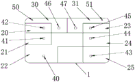
For easy understanding, referring to fig. 1, an embodiment of the invention provides a dual-interface security chip card, including: an insulating substrate 1;
the insulating substrate 1 includes a first surface and a second surface disposed opposite to the first surface;
the surface of the first surface is plated with gold, the first surface is provided with a plurality of contact points 20, 21, 22, 23, 24, 25 and non-contact points 30, 31, wherein the non-contact points 30, 31 are arranged outside the range of the interface position specified by the ISO7816 standard and are used for supporting the contact points 20, 21, 22, 23, 24, 25 to correspond to the interface position specified by the ISO7816 standard.
It will be appreciated that the contact contacts 20, 21, 22, 23, 24, 25 and the non-contact points 30, 31 are defined by metal etching on the first side of the insulating substrate 1.
Referring to fig. 2, fig. 2 is a schematic diagram of the positions of contacts specified in the ISO7816 specification, when the left edge and the upper edge of the front surface of the substrate are taken as a reference, the distance range of the contacts C1, C2, C3, and C4 from the left edge is 10.25-12.25cm, the distance range of the contacts C1 and C5 from the upper edge is 19.23-20.93cm, the distance range of the contacts C2 and C6 from the upper edge is 21.77-23.47cm, the distance range of the contacts C3 and C7 from the upper edge is 24.31-26.01cm, the distance range of the contacts C4 and C8 from the upper edge is 26.85-28.55cm, the distance range of the contacts C5, C6, C7, and C8 from the left edge is 17.87-19.87cm, meanwhile, the contacts C1-C8 represent different interfaces respectively, the VCC interface defined in the ISO7816 specification represents a power supply Voltage (VCC) interface, and a reset interface (CLK) represents a C599 interface, contacts C4 and C8 each represent a reserved interface, contact C5 represents a Ground (GND) interface, contact C6 represents a programming Voltage (VPP) interface, and contact C7 represents an input/output (I/O) interface. In the present embodiment, the number of the contact contacts 20, 21, 22, 23, 24, and 25 is 6, and the positions of the contacts C1 to C8 may be respectively corresponding according to functions and definitions, so that the contact contacts 20, 21, 22, 23, 24, and 25 conform to the position distribution specified in the ISO7816 specification, and may be compatible with various types of card readers; in addition, the non-contact points 30 and 31 do not occupy the positions of the contact points 20, 21, 22, 23, 24 and 25, so that the layout design is facilitated, different production processes can be met, and the process difficulty is reduced;
wherein, the non-contact points 30 and 31 are one pair or two pairs;
the contact contacts 20, 21, 22, 23, 24, 25 or the non-contact contacts 30, 31 are insulated from each other.
The contact contacts 20, 21, 22, 23, 24 and 25 are used for the contact conduction of the double-interface security chip card and the card reader;
further, referring to fig. 3, the second side is provided with the chip 6, the non-contact points 30, 31 are connected with the corresponding first contacts of the chip 6 through the wires 9, and the contact contacts 20, 21, 22, 23, 24, 25 are connected with the corresponding second contacts of the chip 6 through the wires 9, so that the chip 6 is electrically operated by reading the card reader;
furthermore, the insulating substrate 1 is provided with a plurality of routing through holes 40, 41, 42, 43, 44, 45, 46 and 47, wherein the routing through holes 40, 41, 42, 43, 44, 45, 46 and 47 are used for the lead 9 to pass through, so that the use of the lead 9 is reduced, the production cost is reduced, and meanwhile, the apertures of the routing through holes 40, 41, 42, 43, 44, 45, 46 and 47 are set according to actual requirements;
further, the non-contact points 30 and 31 are deposited or coated on a preset non-pad area of the second surface through a conductive medium, and meanwhile, the non-pad area is used for forming pads 70 and 71 through the deposition or coating of the conductive medium, wherein the non-pad area can be randomly selected on the second surface according to the card manufacturing requirement, after the non-contact points 30 and 31 are connected with the pads 70 and 71 through the deposition or coating, the pads 70 and 71 are connected with the chip 6, and the pads 70 and 71 are used for connecting an antenna, so that the double-interface secure chip card realizes non-contact communication;
it should be noted that the deposition and coating method is the prior art, and is not described herein; the deposition or coating amount of the bonding pads 70, 71 is set according to the requirement, and is not limited herein; meanwhile, the shapes of the bonding pads 70 and 71 and the relative positions on the insulating substrate 1 are not limited so as to adapt to the process design;
it can be understood that the connection difficulty between the pads 70, 71 and the non-contact points 30, 31 is greatly reduced by the deposition or coating method in the embodiment, the size and the position of the pads 70, 71 can be set according to the requirement, the use area of the insulating substrate 1 of the second surface is saved, and meanwhile, the pads 70, 71 are externally connected with the antenna without slotting connection, thereby reducing the process difficulty; in addition, only the first surface needs to be plated with gold, so that the production cost is reduced.
Furthermore, the insulating substrate 1 is provided with a plurality of pad holes 50 and 51 for the conductive medium 8 to pass through, the aperture of the pad holes 50 and 51 is set according to the actual requirement, but the aperture of the pad holes 50 and 51 is not larger than the aperture of the routing through holes 40, 41, 42, 43, 44, 45, 46 and 47, the conductive medium 8 can be deposited or coated on the pad holes 50 and 51 from the non-contact points 30 and 31, and then deposited or coated on the non-contact pad region preset on the second surface from the pad holes 50 and 51, so that the deposition or coating path is shortened, the use of the conductive medium 8 is reduced, the production cost is reduced, and the process production is facilitated.
Further, the conductive medium 8 may be made of epoxy resin paste containing conductive metal such as gold, copper, silver, or other conductive material.
Further, the number of the pads 70, 71 is two;
further, the chip 6, the first contact and the second contact on the second surface of the insulating substrate 1 are wrapped with an encapsulating adhesive, so that the chip 6, the first contact, the second contact and the wire 9 are protected.
Example two
The second embodiment provides a method for manufacturing a dual-interface security chip card on the basis of the first embodiment, and with reference to fig. 4, the method includes:
s101: the first surface of the insulating substrate 1 after gold plating treatment is divided into a plurality of contact contacts 20, 21, 22, 23, 24, 25 and non-contact points 30, 31 by etching, wherein the contact contacts 20, 21, 22, 23, 24, 25 are distributed in positions according to ISO7816 specifications so as to support various types of card readers;
s102: attaching the chip 6 to the second surface of the insulating substrate 1, connecting the non-contact points 30 and 31 to corresponding first contacts on the chip 6 through wires, and connecting the contact points 20, 21, 22, 23, 24 and 25 to corresponding second contacts on the chip 6 through wires;
s103: the pads 70, 71 are formed by depositing or coating a conductive medium on the non-pad areas predetermined on the second side from the non-contact points 30, 31, and the pads 70, 71 are connected to the antenna.
Preferably, step S103 specifically includes: pad holes 50 and 51 are formed in the insulating substrate, non-contact points 30 and 31 are deposited or coated on the pad holes 50 and 51 through conductive media, then the non-contact pad areas are deposited or coated on the second surface from the pad holes 50 and 51 through the conductive media, pads 70 and 71 are formed in the non-contact pad areas through the conductive media, and the pads 70 and 71 are connected with the antenna.
It can be clearly understood by those skilled in the art that, for convenience and brevity of description, the specific working processes of the system and the module described above may refer to the corresponding processes in the foregoing method embodiments, and are not described herein again.
In the several embodiments provided in the present application, it should be understood that the disclosed system, apparatus and method may be implemented in other manners. For example, the above-described apparatus embodiments are merely illustrative, and for example, the division of the modules is merely a logical division, and in actual implementation, there may be other divisions, for example, multiple modules or components may be combined or integrated into another system, or some features may be omitted, or not implemented. In addition, the shown or discussed mutual coupling or direct coupling or communication connection may be an indirect coupling or communication connection through some interfaces, devices or modules, and may be in an electrical, mechanical or other form.
The above-mentioned embodiments are only used for illustrating the technical solutions of the present invention, and not for limiting the same; although the present invention has been described in detail with reference to the foregoing embodiments, it will be understood by those of ordinary skill in the art that: the technical solutions described in the foregoing embodiments may still be modified, or some technical features may be equivalently replaced; and such modifications or substitutions do not depart from the spirit and scope of the corresponding technical solutions of the embodiments of the present invention.
Claims (10)
1. A double-interface security chip card comprises an insulating substrate, and is characterized in that the insulating substrate comprises a first surface and a second surface arranged opposite to the first surface;
the surface of the first surface is subjected to gold plating treatment, and the first surface is provided with a plurality of non-contact points;
the second surface is provided with a chip, and the non-contact point is connected with a corresponding first contact of the chip through a lead;
the non-contact point is deposited or coated on a non-bonding pad area preset on the second face through a conductive medium, the non-bonding pad area is used for forming a bonding pad through deposition or coating of the conductive medium, and the bonding pad is used for connecting an antenna.
2. The dual interface security chip card of claim 1, wherein said first side is provided with a plurality of contact contacts, said contact contacts being connected to corresponding second contacts of said chip by wires.
3. The dual interface security chip card of claim 2, wherein said contactless contacts are disposed outside the range of interface locations specified by the ISO7816 specification for supporting the contact contacts to correspond to the interface locations specified by the ISO7816 specification.
4. The double-interface security chip card according to claim 2 or 3, characterized in that the individual contact contacts or the non-contact contacts are insulated from each other.
5. The dual-interface security chip card of claim 1 or 2, wherein said insulating substrate has a plurality of wire-bonding through holes for said wires to pass through.
6. The double-interface security chip card of claim 1, wherein said insulating substrate is provided with a plurality of pad holes for passing said conductive medium.
7. The dual interface security chip card of claim 1 or 6, wherein said conductive medium is an epoxy glue containing a conductive metal.
8. The dual interface security chip card of claim 2, wherein said chip, said first contact and said second contact are encapsulated with an encapsulating adhesive.
9. A method for manufacturing a dual-interface security chip card according to claims 1 to 8, comprising:
s101: etching the first surface of the insulating substrate after gold plating treatment to divide the first surface into a plurality of contact points and non-contact points;
s102: attaching a chip to a second surface of the insulating substrate, and connecting the non-contact points with corresponding first contacts on the chip through wires, and connecting the contact contacts with corresponding second contacts of the chip through wires;
s103: and a conductive medium is deposited or coated on a non-bonding pad area preset on the second surface from the non-contact point, a bonding pad is formed in the non-bonding pad area through the deposition or coating of the conductive medium, and the bonding pad is connected with the antenna.
10. The method for manufacturing a dual-interface security chip card according to claim 9, wherein the step S103 specifically comprises: and arranging a pad hole on the insulating substrate, depositing or coating a conductive medium from the non-contact point to the pad hole, depositing or coating the conductive medium from the pad hole to a non-bonding pad area preset on the second surface, depositing or coating the conductive medium on the non-bonding pad area to form the bonding pad, and connecting the bonding pad with the antenna.
Priority Applications (1)
| Application Number | Priority Date | Filing Date | Title |
|---|---|---|---|
| CN202010477447.3A CN111626395A (en) | 2020-05-29 | 2020-05-29 | Double-interface security chip card and manufacturing method thereof |
Applications Claiming Priority (1)
| Application Number | Priority Date | Filing Date | Title |
|---|---|---|---|
| CN202010477447.3A CN111626395A (en) | 2020-05-29 | 2020-05-29 | Double-interface security chip card and manufacturing method thereof |
Publications (1)
| Publication Number | Publication Date |
|---|---|
| CN111626395A true CN111626395A (en) | 2020-09-04 |
Family
ID=72272327
Family Applications (1)
| Application Number | Title | Priority Date | Filing Date |
|---|---|---|---|
| CN202010477447.3A Pending CN111626395A (en) | 2020-05-29 | 2020-05-29 | Double-interface security chip card and manufacturing method thereof |
Country Status (1)
| Country | Link |
|---|---|
| CN (1) | CN111626395A (en) |
Cited By (1)
| Publication number | Priority date | Publication date | Assignee | Title |
|---|---|---|---|---|
| CN114169484A (en) * | 2021-12-14 | 2022-03-11 | 中国工商银行股份有限公司 | Double-chip transaction card and multi-chip transaction card |
Citations (5)
| Publication number | Priority date | Publication date | Assignee | Title |
|---|---|---|---|---|
| CN101095220A (en) * | 2004-12-28 | 2007-12-26 | Ask股份有限公司 | Double-sided electronic module for hybrid smart card |
| CN106415613A (en) * | 2014-05-14 | 2017-02-15 | 兰克森控股公司 | Method for producing a circuit for a chip card module and circuit for a chip card module |
| US20170077590A1 (en) * | 2014-03-03 | 2017-03-16 | Smart Packaging Solutions | Simplified electronic module for a smartcard with a dual communication interface |
| CN108496187A (en) * | 2016-01-26 | 2018-09-04 | 兰克森控股公司 | Method for manufacturing chip card module and chip card |
| CN109729733A (en) * | 2017-08-28 | 2019-05-07 | 智能科技私人有限公司 | Integrated circuit module and smart card including the same |
-
2020
- 2020-05-29 CN CN202010477447.3A patent/CN111626395A/en active Pending
Patent Citations (5)
| Publication number | Priority date | Publication date | Assignee | Title |
|---|---|---|---|---|
| CN101095220A (en) * | 2004-12-28 | 2007-12-26 | Ask股份有限公司 | Double-sided electronic module for hybrid smart card |
| US20170077590A1 (en) * | 2014-03-03 | 2017-03-16 | Smart Packaging Solutions | Simplified electronic module for a smartcard with a dual communication interface |
| CN106415613A (en) * | 2014-05-14 | 2017-02-15 | 兰克森控股公司 | Method for producing a circuit for a chip card module and circuit for a chip card module |
| CN108496187A (en) * | 2016-01-26 | 2018-09-04 | 兰克森控股公司 | Method for manufacturing chip card module and chip card |
| CN109729733A (en) * | 2017-08-28 | 2019-05-07 | 智能科技私人有限公司 | Integrated circuit module and smart card including the same |
Cited By (1)
| Publication number | Priority date | Publication date | Assignee | Title |
|---|---|---|---|---|
| CN114169484A (en) * | 2021-12-14 | 2022-03-11 | 中国工商银行股份有限公司 | Double-chip transaction card and multi-chip transaction card |
Similar Documents
| Publication | Publication Date | Title |
|---|---|---|
| US6568600B1 (en) | Chip card equipped with a loop antenna, and associated micromodule | |
| US10810477B2 (en) | Method for producing a circuit for a chip card module and circuit for a chip card module | |
| US10229888B2 (en) | Systems and methods for providing electromagnetic interference (EMI) compartment shielding for components disposed inside of system electronic packages | |
| US7855895B2 (en) | Universal PCB and smart card using the same | |
| US9390365B2 (en) | Integrated circuit module for a dual-interface smart card | |
| US8546927B2 (en) | RFIC chip mounting structure | |
| RU98115301A (en) | ELECTRONIC CONTACTLESS MODULE FOR CARD OR LABEL | |
| CN103681371A (en) | Silica-based wafer level fan-out encapsulation method and silica-based wafer level fan-out encapsulation structure | |
| CN1952958A (en) | Method for fabricating and packaging chips and elements to smart card with plastic package technique | |
| US9424507B2 (en) | Dual interface IC card components and method for manufacturing the dual-interface IC card components | |
| CN111626395A (en) | Double-interface security chip card and manufacturing method thereof | |
| KR102014621B1 (en) | Method for producing a single-sided electronic module including interconnection zones | |
| JP4240990B2 (en) | IC module circuit board | |
| CN208781268U (en) | A kind of list interface stripe cell, single interface band, module and smart card | |
| CN116235179A (en) | Circuit for smart card chip module, smart card chip module and method for manufacturing smart card chip module | |
| CN108764436A (en) | A kind of list interface stripe cell, single interface band, module and smart card | |
| JP4471926B2 (en) | Semiconductor device | |
| TWI606401B (en) | Smart card, smart card contact pad carrier board and manufacturing method thereof | |
| CN210015456U (en) | A dual interface card and its dual interface module | |
| CN210955154U (en) | Miniature 6 pad smart card modules | |
| KR100530760B1 (en) | Contactless IC card and method for manufacturing the same | |
| EP3079105B1 (en) | Dual-interface ic card components and method for manufacturing the dual-interface ic card components | |
| CN118043817A (en) | IC module and method for manufacturing IC module | |
| KR100503048B1 (en) | How to make contactless IC card | |
| WO2024196307A1 (en) | Articles of manufacture relating to ic modules and smart cards |
Legal Events
| Date | Code | Title | Description |
|---|---|---|---|
| PB01 | Publication | ||
| PB01 | Publication | ||
| SE01 | Entry into force of request for substantive examination | ||
| SE01 | Entry into force of request for substantive examination | ||
| RJ01 | Rejection of invention patent application after publication |
Application publication date: 20200904 |
|
| RJ01 | Rejection of invention patent application after publication |