Abstract
The scalability of integrated photonics hinges on low-loss chip-scale components, which are important for classical applications and crucial in the quantum domain. An important component is the power splitter, which is an essential building block for interferometric devices. Here, we use inverse design by topology optimization to devise a generic design framework for developing power splitters in any material platform, although we focus the present work on silicon photonics. We report on the design, fabrication, and characterization of silicon power splitters and explore varying domain sizes and wavelength spans around a center wavelength of 1550 nm. This results in a set of power splitters tailored for ridge, suspended, and embedded silicon waveguides with an emphasis on compact size and wide bandwidths. The resulting designs have a footprint of  and exhibit remarkable 0.5 dB bandwidths exceeding 300 nm for the ridge and suspended power splitters and 600 nm for the embedded power splitter. We fabricate the power splitters in suspended silicon circuits and characterize the resulting devices using a cutback method. The experiments confirm the low excess loss, and we measure a 0.5 dB bandwidth of at least 245 nm—limited by the wavelength range of our lasers.
Export citation and abstract BibTeX RIS

Original content from this work may be used under the terms of the Creative Commons Attribution 4.0 license. Any further distribution of this work must maintain attribution to the author(s) and the title of the work, journal citation and DOI.
1. Introduction
The unique properties of light make it an attractive platform for quantum technologies. Chip-scale quantum photonic circuits [1] leverage the scalability of semiconductor technology as well as the rapidly growing insights from research on nanophotonics [2] to enable highly efficient interfaces with matter [3] for, e.g. quantum nonlinearities [4], and squeezed light sources [5]. Minimizing losses is key to quantum photonics, which has led to the exploration of materials such as silicon nitride and lithium niobate, whose nanofabrication methods are much less mature than those for silicon but which instead offer ultra-low propagation losses in photonic waveguides [6, 7]. In addition, photonic waveguides may be suspended, embedded, or simply reside as ridge or rib waveguides on substrates with a lower refractive index, and the different materials are subject to different fabrication constraints. This calls for a generic optimization framework capable of devising highly optimized components across all materials, geometries, and fabrication constraints.
Large-scale integrated quantum photonic devices require the development of photonic circuit components exhibiting unparalleled performance with a compact footprint. Since the spatial modes of light are the same across the quantum and the classical domains [8], the challenge of building low-loss components is an optimization problem governed by Maxwell's equations. Such optimizations can be approached by size and shape optimization on geometries based on simple designs, but they can typically only compete with advanced inverse-design methods in the simplest cases. Generally, the most rewarding scenarios for inverse design involve structures optimized for multiple mutually dependent figures of merit or unclear performance bounds [9], where intuition-based approaches cannot realistically succeed. Examples include mode-converters [10–14], non-reciprocal routers [15], circuit crossings [16], high-spatial-confinement cavities [17], metalenses [13, 18–20] and demultiplexers [21–23]. Even for design challenges traditionally dominated by intuition-based approaches, such as grating couplers, mirrors, waveguide bends, and beam splitters, inverse design can offer significant improvements by minimizing footprints [24–26] and extending bandwidths [27, 28]. Here we are concerned with the inverse design of compact, highly efficient, broadband, 50:50 power splitters, which are essential devices in both quantum photonic architectures [29–31] and classical applications such as signal routing [32], spectroscopy [33], and imaging [34]. Our method applies to any material platform, but we consider silicon, which offers advanced fabrication technology and integration with electronics and nanomechanics [35]. Silicon is gaining attention for quantum technologies not only for the aforementioned reasons but also due to the ability to integrate emitters with excellent quantum optical and spin properties [36, 37].
The 50:50 power splitters mainly fall into two categories: as specialized instances of generic  couplers, such as directional couplers, or as fixed power-splitting devices with a
  configuration [38]. Directional couplers are the chip-scale equivalent of a conventional optical beam splitter, and they operate by evanescent coupling of the modes of two adjacent waveguides separated by a small gap, with the power distribution along them and the final power-splitting ratio determined by the width of that gap, the optical interaction length, and the wavelength. That ratio can be tuned by refractive-index changes, achieved via thermo-optic or electro-optic effects, or by modifications to the gap through mechanical actuation if the waveguides are suspended. Such tunability makes them ideal for optical switching in programmable networks. Nevertheless, their dispersive working mechanism makes them sensitive to deviations of the fabricated structure from the nominal geometry, thus requiring post-fabrication calibration to achieve the targeted 50:50 splitting [39, 40]. On the other hand, the
  power splitters are robust to size variations and more broadband, making them ideal for Mach–Zehnder interferometers (MZIs) or cascaded
  power splitters. A possible intuitive design is a Y-splitter with a gradual (adiabatic) geometry transition from one waveguide into two waveguides [41, 42]. The simple adiabatic Y-splitters can have good bandwidth (400 nm) and low intrinsic losses, but the required footprint limits their use in large-scale nanophotonic networks and sets demanding requirements in terms of the extrinsic propagation losses associated with fabrication disorder. The propagation loss is often only considered for waveguides but must also be taken into account when other components get exceedingly long.
A multitude of design approaches has been applied to silicon power splitters [24, 43–50] and has resulted in remarkable improvements over the past decades. Table 1 summarizes the previously reported Y-splitter designs, including their center excess loss, bandwidth (defined as where the excess loss does not exceed 0.5 dB), and the corresponding sizes. Low excess losses have been reported with slot-waveguide Y-splitters featuring a center excess loss of only 0.06 dB and more than 100 nm bandwidth for a length of 40 µm [43]. In terms of bandwidth, Y-splitter designs featuring more than 700 nm with a length of 5 µm have been theoretically proposed [50] although this included sharp features that can hardly be realized experimentally. Compact Y-splitters with lengths down to 0.9 µm have been devised by 2D inverse design [24], 1.5 µm with compact star-shape splitters [44], and approximately 3 µm with size optimization of the tapering region in Y-splitters [45, 46]. However, these compact Y-splitter designs do not display bandwidths larger than 100 nm. More generally, a power-splitter that simultaneously exhibits low loss, wide bandwidth, and compact footprint has so far been missing. In this study, we explore the achievable performance in terms of size, loss, and bandwidth of power splitters by employing density-based topology optimization [51, 52]. This inverse design method optimizes the refractive indices in a large material grid without putting any restrictions on the device shape or topology besides the resolution of the material grid. The vast design space explored by inverse-design methodologies frequently leads to record-breaking performance [24–26, 28, 50, 53–55], but may in some cases contain unfeasible design elements [50, 54]. More recent works on inversely designed structures include the fabrication constraints directly in the optimization, e.g. the resolution, the minimum solid and void radii of curvature, or the feature-size dependence of the pattern transfer fidelity. This approach harvests the benefits of inverse design while resulting in geometries that are inherently realistic [17, 27, 56, 57]. In this study, we ensure that the final designs respect fabrication restrictions of electron beam lithography with an explicit constraint on ensuring connectivity of free-standing (suspended) structures as well as implicitly through parameters such as smoothing radius [58, 59] and design-element size. We design broadband and compact power splitters with a center wavelength of 1550 nm for three different photonic platforms: embedded, ridge, and suspended. We fabricate the suspended version in a silicon membrane as shown in figure 1(a). The high design-to-device fidelity results in a very good agreement between simulated and measured performance across a very wide wavelength span (figure 1(b)).
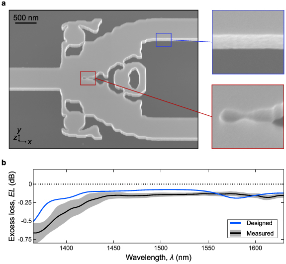
Figure 1. Compact and broadband topology-optimized power splitters. (a) Tilted-view scanning electron micrograph of a fabricated power splitter with insets highlighting specific design features. (b) The measured mean excess loss with (black solid) and 95% confidence interval (shaded) shows very good agreement with the simulated performance (blue) within the measured wavelength range available with the two tunable lasers used in our experiment.
Download figure:
Standard image High-resolution imageTable 1. Measured performance and figures of merit of power splitters reported in the literature compared to this work. The power splitters are listed based on the number of channels, the waveguide type, the optimization procedure (parametric, size, or topology optimization), the size, the center excess loss and the 0.5 dB bandwidth. The measured bandwidths denoted with * are limited by the wavelength range in the experiment.
| Channels | Type | Optimization procedure | Size (µm2) |
 (dB) (dB) | 0.5 dB BW (nm) | Reference |
|---|---|---|---|---|---|---|

| Embedded | Parametric |

| −0.06 | 100* | [43] |

| Embedded | Parametric |

| −0.5 | — | [44] |

| Embedded | Size |

| −0.28 | 80* | [45] |

| Embedded | Size |

| −0.1 | 45* | [46] |

| Embedded | Topology |

| −0.5 | — | [24] |

| Embedded | Topology |

| −0.44 | 90 | [57] |

| Suspended | Topology |

|

| 245* | This work |
2. Model formulation
We model power splitters between one input waveguide and two output waveguides, each with a width, w, as shown in figure 2. The waveguides are connected to a rectangular design domain of length L and width W. We denote the waveguide material as the core material, while the surrounding material is denoted as the cladding material. We simulate the transfer of light from the input waveguide to the two output waveguides by solving the electromagnetic wave equation in the frequency domain:

where  is the spatial profile of a time-harmonic electric field of angular frequency ω,
  is the complex refractive index of the material, and c is the speed of light in vacuum. We consider the fundamental transverse-electric mode of the waveguide, which we insert as a source in the input port (Port 1 in figure 2) and simulate the transfer of light into the same mode for the two output waveguides (Ports 2 and 3). The boundaries of the model are truncated by using a first-order absorbing boundary condition,

which allows light to escape out of the model domain while limiting reflections. In addition, we use perfectly matched layers at the outer ends of the waveguide domains,  , in order to absorb directly transmitted or back-reflected light. We solve the electromagnetic problem with the finite-element method in the commercial software COMSOL Multiphysics® v. 6.0 [60].
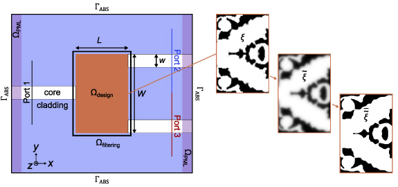
Figure 2. Implementation of power splitter model. The illustration on the left shows the model domain, wherein the design domain of the power splitter is highlighted with the brown rectangle in the center. The design field, ξ, is defined in the design domain to control the material distribution. The panels on the right show the evolution of the design field through the smoothing and thresholding steps defined in equations (4)–(7).
Download figure:
Standard image High-resolution image3. Optimization
We aim to design a set of power splitters that operate efficiently over a user-specified bandwidth, exhibiting ideally a perfect balance between the output channels (by imposing device symmetry), maximum power transfer, and minimum back-reflection into the input waveguide. To this end, we define the objective function,

which is tailored to promote high broadband transmission at the output ports (Port 2 and 3) and low reflection at the input port (Port 1). To ensure a wide wavelength span, we consider the transmission, T, and reflection, R, of the power splitter for three wavelengths,  . The sum in equation (3) includes the scaling factors,
  , the values of which are chosen empirically to emphasize the performance at the center wavelength. We employ density-based topology optimization as described in [61] to optimize the material distribution within the designated design domain. We define a design field, ξ, that can vary continuously between 0 and 1 to interpolate between the core and cladding material in the design domain, i.e.

Then, we perform a smoothing step on the design field to limit the appearance of small design features and prevent a mesh-dependent solution. The smoothed design field,  , is created with a density-filter operation [62], which is defined via

with a smoothing radius,  of 100 nm. Then we employ a smoothed approximation of the Heaviside function,

that transforms the design field towards binary values close to 0 or 1 to realize realistic designs of either cladding or core material. The parameter η defines the threshold in the function, whereas the parameter β controls the threshold sharpness. We apply the threshold operation (equation (6)) on the smoothed design field with the threshold being at the center value–η = 0.5:

We progressively double the threshold sharpness starting from 5 and ending at 80 using a continuation approach to achieve a near-binary design [58]. The three design-field steps (ξ,  , and
, and  ) are illustrated in the right panels of figure 2. We use the thresholded design field,
  , to interpolate into a refractive-index distribution in the design domain with a linear material interpolation between the core and cladding materials,

To further promote a binary design, we introduce an artificial extinction coefficient,  , defined in equation (9) that causes optical losses for intermediate values of the thresholded design field [63]. In conjunction, we directly impose a limit on the non-binary design in equation (10) with an inequality constraint that requires the losses in the design domain to be less than a constant,
  ,
,

The refractive index and extinction coefficient are inserted into the wave equation, which is solved to compute the electric field distribution used to calculate the optical performance of the device as quantified by the objective function in equation (3).
The evolution of the geometry and the objective function during an optimization run are illustrated in figure 3 for a power splitter with a design domain size of  m and optimized at the wavelengths,
 ![$\lambda_{i}\in [1450\,\textrm{nm}, 1550\,\textrm{nm}, 1650\,\textrm{nm}]$](https://content.cld.iop.org/journals/2633-4356/4/1/016201/revision3/mqtad2521ieqn36.gif) . The design field is initialized with ξ = 0.5, i.e. a material with properties between silicon and air. A Y-splitter form appears early in the design iterations, which guides light towards the output waveguides. The optimization improves the coupling by further shaping the Y-splitter and forming guiding antenna-like structures on the sides to direct back-scattered light toward the output waveguides. The objective function increases rapidly in the first 50 iterations and slows down as it gets closer to the local optimum. The notable jumps in the objective value at different continuation steps with different β stem from the artificial attenuation (equation (9)), which is set to penalize grey-scale by increased losses, and its impact gradually diminishes as the thresholding parameter, β, increases.
. The design field is initialized with ξ = 0.5, i.e. a material with properties between silicon and air. A Y-splitter form appears early in the design iterations, which guides light towards the output waveguides. The optimization improves the coupling by further shaping the Y-splitter and forming guiding antenna-like structures on the sides to direct back-scattered light toward the output waveguides. The objective function increases rapidly in the first 50 iterations and slows down as it gets closer to the local optimum. The notable jumps in the objective value at different continuation steps with different β stem from the artificial attenuation (equation (9)), which is set to penalize grey-scale by increased losses, and its impact gradually diminishes as the thresholding parameter, β, increases.
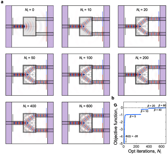
Figure 3. Progression of design and electric field distribution during 2D topology optimization of a power splitter with a  m2 design domain and 200 nm optimization wavelength span. (a) The design and electric field distribution at select iterations, N, are shown to illustrate the progression toward the final design. (b) The iteration history of the objective function for the various continuation steps with different threshold values, β.
Download figure:
Standard image High-resolution imageThe optimization problem, as defined by equations (1)–(10), is sufficient to optimize power splitter structures in the ridge and embedded platforms. However, for power splitters fully suspended in air, we require another constraint to ensure that all material regions are connected to the waveguide for the device to be physically realizable. Therefore, we implement a connectivity constraint [14, 64] with an auxiliary heat problem, where heat is only removed if the material connects to the input waveguide. We define a conductivity parameter, σ,

where  is the area of the design domain and σcore and σcladding are conductivities set for the core and cladding region. We use a high conductivity in the solid regions and a low conductivity in the air region. Similarly, we define a heat source,
  , with an interpolation of the double-thresholded design field and high heat generation in the solid regions,
  and no heat generation in air,
  ,
,

We solve the heat equation in the design domain,


with a zero-Dirichlet boundary condition on the connected input waveguide and zero-Neumann boundary condition elsewhere to find the field, u, which represents the local heat density. We compare the total heat in the design domain to the heat in a reference domain of equal size and made of the solid material and limit the logarithmic heat ratio to a set value  with an inequality constraint,
The full optimization problem is solved using the algorithm known as the globally convergent method of moving asymptotes [65] and employing the adjoint sensitivity method for computing the gradient of the design field [66].
4. Optimization results
First, we investigate the role of the selected optimization wavelengths,  , on the achievable operational bandwidth of an inversely designed power splitter. Due to the large computational load of 3D simulations [67], this study uses optimization in 2D with a homogeneous air cladding to find good optimization parameters for the subsequent full optimization in 3D. We perform three independent optimizations for three different optimization wavelength spans,
  , defined as the range between the outer optimization wavelengths. The wavelength spans are set to the following: 1 nm to mimic a single-wavelength optimization, 200 nm to get a moderate bandwidth, and finally 400 nm, which is similar to the highest previously reported bandwidths [43, 68]. The design domain is set to be
  m and the waveguide width is w = 500 nm. The performance of the power splitters is evaluated based on the excess loss (EL), return loss (RL), bandwidth, and size, where EL is defined as the ratio of power coupled to the output waveguides to the input power, and RL represents the ratio of back-reflected power to the input power. We consider the bandwidth to be the wavelength range for which the EL is less than 0.5 dB.
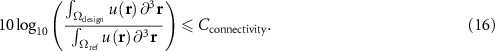
The final designs and their performance are shown in figure 4. We observe that the optimization with  = 1 nm exhibits a broadband response, especially in transmission, achieving a 0.5 dB bandwidth of 406 nm, which may explain the success of other design optimizations that have used a single-wavelength objective function [45]. The optimization with
  = 200 nm shows a flatter loss spectrum as the multiple optimization wavelengths are close to each other. Despite the larger
  , the optimized geometry does not exhibit a wider bandwidth. On the contrary, the optimization for
  = 400 nm leads to a record-high bandwidth of 656 nm. However, the EL drops significantly between the optimization wavelengths. This is a consequence of the optimization only enforcing a high performance at the specified optimization wavelengths. This could be mitigated by increasing the number of wavelengths albeit at the expense of more computation time. While resonant-like features in transmission at the optimization wavelengths are limited, the reflections exhibit features at or close to the optimization wavelengths, particularly for
  1 nm, for which a large 10 dB dip is visible. Despite that, the optimization achieves nearly zero EL and low reflections of −30 dB (0.1%) or less at the optimization wavelengths. The three optimized geometries exhibit many common features: they all have a characteristic V-shape, some narrow beams in between, and an antenna-like shape on the input side. The beams serve the dual purpose of suppressing reflection at the branching point and preventing direct forward propagation. At the same time, the structure at the input guides scattered waves originating from the center of the design region into the output waveguides. We find that all features positively impact the objective function, albeit leading to multiple dips at other wavelength ranges due to resonant wave phenomena.
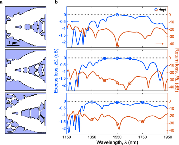
Figure 4. Two-dimensional optimization of power splitters with different optimization wavelength spans. The design (a) and the performance (b) are shown for three optimization runs of power splitters targeting bandwidths of 1 nm, 200 nm and 400 nm.
Download figure:
Standard image High-resolution imageTo further understand the achievable performance and its relation to the size of the power splitters, we perform 2D optimizations of air-cladded power splitters of domain lengths  . The optimization wavelength span is set to 200 nm as the previous simulations show that this achieves the most uniform performance around the center wavelength. The resulting geometries and transmission/reflection spectra are shown in figure 5. We find a degradation of the objective function value for the 1 µm × 3 µm design domain. However, its 0.5 dB bandwidth extends almost 100 nm longer than the same optimizations with a longer length. In addition, both EL and RL display fewer narrow features, which suggests, as does the optimized geometry, that the size limits the presence of minute resonant features. On the contrary, both the 2 and 3 µm long power splitters exhibit several narrow geometric features, which play a key role in minimizing the EL at the targeted wavelengths. Interestingly, the power splitter with a
  m footprint exhibits the lowest objective function value (see table 2) despite being encompassed by the larger domain size. This observation indicates both the abundance of local optima and the responsiveness of the optimization process to the scale of design components.
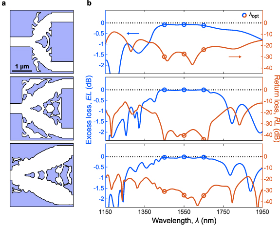
Figure 5. Two-dimensional optimization of power splitters with different design-domain lengths. The design (a) and the performance (b) are shown for three optimization runs with design-domain lengths of 1, 2, and 3 µm, while the optimization wavelength span is set to 200 nm.
Download figure:
Standard image High-resolution imageTable 2. Comparison of power splitter optimizations with various design inputs. The power splitters are listed by model dimension, waveguide type, size of design domain, and optimization wavelength span,  . The objective function,
  , quantifies the optimization performance, while the device characteristics are: the center excess loss,
  ; the center return loss,
  ; the bandwidth with excess loss below 0.5 dB; and the highest return loss,
  , for that bandwidth.
| Model | Type | Size (µm2) |
 (nm) (nm) |
 (dB) (dB) |
 (dB) (dB) |
 (dB) (dB) | 0.5 dB BW (nm) |
 (dB) (dB) |
|---|---|---|---|---|---|---|---|---|
| 2D | air-cladded |

| 1 | −0.004 | −0.004 | −42.98 | 406 | −18.91 |
| 2D | air-cladded |

| 200 | −0.100 | −0.076 | −27.57 | 484 | −18.82 |
| 2D | air-cladded |

| 200 | −0.003 | −0.002 | −40.44 | 353 | −20.59 |
| 2D | air-cladded |

| 200 | −0.028 | −0.020 | −34.21 | 397 | −19.59 |
| 2D | air-cladded |

| 400 | −0.082 | −0.083 | −31.31 | 656 | −17.35 |
| 3D | ridge |

| 200 | −0.139 | −0.121 | −36.48 | 325 | −19.01 |
| 3D | embedded |

| 200 | −0.114 | −0.107 | −38.09 | 629 | −17.93 |
| 3D | suspended |

| 200 | −0.115 | −0.102 | −32.72 | 317 | −20.17 |
While 2D simulations provide good intuition by outlining the design space, they fail to capture out-of-plane scattering losses which may dominate in planar-integrated photonic splitters. In addition, 2D simulations rest on the assumption of a homogeneous effective refractive index—an assumption that is generally not valid in complex nanostructures. Therefore, we perform 3D optimization using the same objective function, which naturally suppresses all loss pathways. The device height is set to 220 nm to match the device layer of conventional photonic silicon-on-insulator wafers. Based on the 2D simulations, we use a  m domain and an optimization wavelength span of 200 nm. In addition, the final thresholded design of the corresponding 2D simulation is used to initialize the design field, except for a modification of the binary design values (ξ = 0 and ξ = 1) into intermediate values (ξ = 0.25 and ξ = 0.75). We run the optimizations for three distinct waveguide platforms: suspended, ridge, and embedded. The suspended power splitter has air surrounding it on all sides, the embedded is covered in glass, and the ridge has glass beneath but air next to and above the structure. The optimized designs and performances for the three waveguide platforms are shown in figure 6. The geometries change considerably compared to the initial 2D design, which stems from the fact that the design also needs to prevent out-of-plane scattering as well as the aforementioned invalidity of the homogeneous assumption about the effective refractive index. Due to out-of-plane scattering, the optimized designs for the various waveguide platforms all share center EL of 0.1 dB compared to the near-zero loss of their 2D counterparts. The ridge and suspended power splitters show a bandwidth of more than 300 nm with a relatively flat EL. The embedded power splitter surpasses these already excellent broadband performances, attaining an unprecedented bandwidth of
  . We attribute this in part to the symmetric electromagnetic environment and in part to the reduced index contrast, which allows for more gentle scattering. In any case, any interpretation must be handled with caution since the model has too many degrees of freedom to make formal inferences about global optimality. We provide a quantitative comparison in table 2 of the simulated figures of merit obtained for all the designed power splitters.
Figure 6. Optimized designs of power splitters made for the ridge, embedded, and suspended waveguide platforms. (a) Side-view illustration of the ridge, embedded, and suspended waveguides fabricated on a silicon-on-insulator platform. (b) Power splitter designs optimized for the various waveguide platforms. (c) The excess loss and return loss as a function of wavelength show excellent broadband performance.
Download figure:
Standard image High-resolution image5. Optical characterization
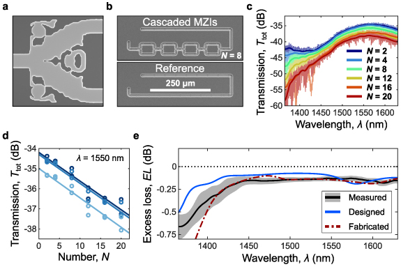
To experimentally validate the performance of the optimized designs, we fabricate the suspended power splitter, a selection driven by its compatibility with our already established suspended silicon platform [17, 69–71]. We fabricate suspended silicon photonic circuits that include the optimized suspended power splitter of figure 6(b) from a silicon-on-insulator substrate with a 220 nm silicon device layer and a 2 µm buried-oxide layer. The pattern is defined using low current (0.22 nA) and high-resolution electron-beam lithography, transferred into a polysilicon/chromium hard mask, and etched into the silicon device layer using a low-power switched  reactive-ion etching process [72, 73]. Then, we remove the buried oxide layer to suspend the circuits with an anhydrous vapor phase hydrofluoric acid etch. An example of a fabricated power splitter is shown in figure 7(a). To validate the simulated EL, we perform broadband optical measurements using two tunable lasers covering a wavelength range from 1365 nm to 1630 nm. We measure on a carefully designed set of circuits with an increasing number of power splitters and use the cutback method to extract the EL per power splitter [45, 70]. Cutback measurements are performed on reference circuits used to find the waveguide propagation loss and on cascaded MZIs which use the power splitter as both a splitter and a combiner (see figure 7(b)). The measurements are performed with a cross-polarized microscope setup using free-space grating couplers placed orthogonally to each other [70]. The measured absolute power transmission for one set of cascaded MZI circuits with an increasing number of MZIs is shown in figure 7(c). We subtract the propagation loss found from the reference measurements and obtain the loss per power splitter via linear fits to the values on a logarithmic scale (dB). Figure 7(d) shows the propagation loss fit for three representative measurement sets of nominally identical photonic circuits. The mean and standard deviation of the extracted EL from 60 measurements (10 measurement sets) are shown in figure 7(e). We find a good agreement with the EL curve of the design except for a small degradation and a 34 nm redshift. To understand this shift, we extract the contour of the fabricated structure from image analysis on five top-view SEM micrographs and simulate each independently. The mean simulated EL of the fabricated structures agrees well with the measured result. The etched features in the fabricated structure have shrunken compared to the original design, which increases the effective refractive index and, therefore, redshifts the spectral response. This indicates robustness towards the growth or shrinkage of the pattern when transferred from design to device, which is commonly observed in nanophotonic components [71].
Figure 7. Experimental validation of suspended power splitters. (a) Scanning electron micrographs of the fabricated suspended power splitter. (b) Scanning electron micrographs of a circuit with Mach–Zehnder loops containing the power splitters and a corresponding reference circuit. (c) Raw measurement data of total transmission through the Mach–Zehnder loop circuits with various lengths and number of power splitters. (d) Cutback measurement of loss per number of power splitters at the center wavelength. (e) The measured excess loss with the mean (black solid) and 95% confidence interval (shaded) compared to the simulated performance of the design (blue) and the mean simulated performance of the fabricated power splitters (red). The wavelength range is limited by the available range of the tunable lasers used in our experiment.
Download figure:
Standard image High-resolution image
6. Conclusion
In summary, we employ topology optimization to design compact and broadband power splitters with hitherto unparalleled performance. We investigate the impact of varying the design domain length and optimization wavelength range in a 2D setting to determine the achievable performance of the power splitters. Using an optimization wavelength span of 400 nm, we obtain a record-high 0.5 dB bandwidth of more than 600 nm. However, with a shorter bandwidth, we obtain a flatter loss profile due to the shorter wavelength spacing. The findings in 2D are used as a starting point for subsequent design optimization in 3D. We design power splitters for three distinct and commonly used waveguide platforms: ridge, embedded, and suspended. Notably, all three platforms demonstrate substantial 0.5 dB bandwidths surpassing 300 nm with the embedded power splitter reaching 600 nm. To validate the realization of the proposed power splitters, we fabricate the device for the suspended waveguide platform and conduct thorough optical characterization to extract the EL. Apart from a redshift caused by fabrication variations, we achieve a remarkable concurrence in the magnitude of the loss and bandwidth. This demonstration further highlights the efficacy of the inverse design method in producing high-performing devices with consistent and desirable characteristics.
Data availability statement
All data that support the findings of this study are included within the article.
Funding
We gratefully acknowledge financial support from the Innovation Fund Denmark (Grant No. 0175-00022 (NEXUS)), The Danish National Research Foundation (Grant No. DNRF147 (NanoPhoton)), the Independent Research Fund Denmark—Natural Sciences (Projects No. 0135-00315 (VAFL)), the European Research Council (Grant No. 101045396 (SPOTLIGHT)), and the European Union's Horizon 2021 research and innovation program under Marie Skłodowska-Curie Action (Grant No. 101067606 (TOPEX)).
Conflict of interest
The authors declare no conflicts of interest.